KEB COMBIVERT F5-A,-E,-H 4.0. APPLICATION MANUAL (2008) - page 5
Operating and Appliance Date
ru.44
Timer 2 display
Adr.
min
max
default
022Ch
0
655,35
0,01
-
-
The count of the free-programmable timer 2 is indicated. The display is done either in seconds, in hours or in slopes/100
(see LE.26). The counter can be adjusted to any chosen value by keyboard or bus. The programming of the counter
is done with the parameters LE.22...LE.26 (also see chapt. 7.15.4 „Timer“).
ru.45
Actual switching frequency
Adr.
min
max
default
022Dh
0
4
1
-
-
Shows the current switching frequency of the inverter. The displayed values correspond to the following switching
frequencies:
0 = 2 kHz
1 = 4 kHz
2 = 8 kHz
3 = 12 kHz
4 = 16 kHz
ru.46
Motor temperature (optionally)
Adr.
min
max
default
022Eh
0
255: off
1
°C
-
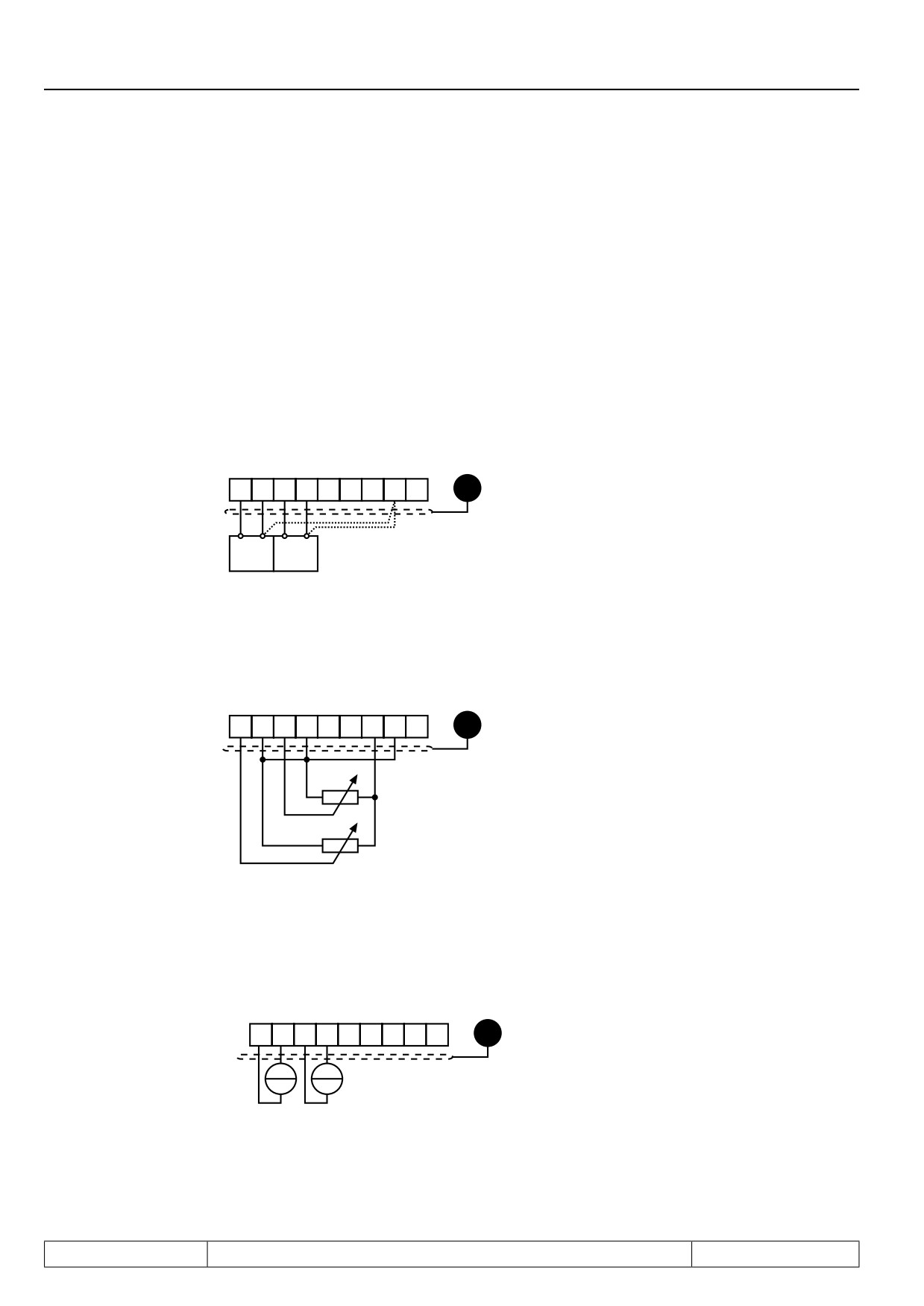
Indicates the current motor temperature. Precondition for this function is aspecial power circuit. The temperature de-
tection is connected to the terminals T1/T2.
0:
T1/T2 closed
253, 254:
cable breakage; short circuit; detection error
255:
T1/T2 open
ru.47
Act. torque limit motor
Adr.
min
max
default
022Fh
-10000
10000
0,01
Nm
-
This parameter indicates the actual adjusted set torque limit for motor operation.
ru.48
Act. torque limit generator
Adr.
min
max
default
0230h
-10000
10000
0,01
Nm
-
This parameter displays the currently adjusted set torque limit for generatoric operation.
Page7.1 - 16
Operating and Appliance Date
ru.49
Actual reference torque
Adr.
min
max
default
0231h
-10000
10000
0,01
Nm
-
This parameter displays the preadjusted setpoint torque at the input of the torque controller.
ru.52
External PID out display
Adr.
min
max
default
0234h
-100,0
100,0
0,1
%
-
A universal PI-controller is integrated into the inverter. It can be used externally as well as internally. So that the controller
is as independent as possible, the displayed manipulated variable, referring to a +/- signal, is output in percent.
ru.53
AUX display
Adr.
min
max
default
0235h
-400,0
400,0
0,1
%
-
The AUX input is setting with An.30. This parameter shows the value of the analog signal AUX in percent. The range
7
of indication is limited to ±400 % (also see Chapt. 6.2 „Analog inputs“).
ru. 54
Actual position
Adr.
min
max
default
0236h
1
Inc
-
-2147483648
2147483647
ru.54 displays the absolute actual position in increments.
ru.56
Set position
Adr.
min
max
default
0238h
-2147483648
2147483647
1
Inc
-
ru.56 displays the absolute set position in increments.
Page7.1 - 17
Operating and Appliance Date
ru.58
Angle difference
Adr.
min
max
default
023Ah
-2147483648
2147483647
1
Inc
-
This parameter displays the actual angular difference between set and actual position.
ru.59
Rotor adaption factor
Adr.
min
max
default
023Bh
0
100
1
%
-
This parameter displays the actual factor of the rotor adaption.
ru.60
Act. position index
Adr.
min
max
default
023Ch
0
255
1
-
-
This parameter displays the actual position index of the position profile.
ru.61
Target position
Adr.
min
max
default
023Dh
-2147483648
2147483647
1
Inc
-
This parameter displays the target position of the actual position index.
ru.63
Profile speed
Adr.
min
max
default
023Fh
-4000
4000
0,125
rpm
-
This parameter displays the speed of the actual position index.
ru.68
Rated DC voltage
Adr.
min
max
default
0244h
0
1000
1
V
-
This parameter shows the rated DC-link voltage automatically determined by the inverter. The value is measured at
switch-on.
ru.69
Distance ref.-zeropoint
Adr.
min
max
default
0245h
-2147483648
2147483647
1
Inc
-
This parameter displays the distance to the zeropoint after relieve the reference switch.
Page7.1 - 18
Operating and Appliance Date
ru.71
Teach/scan position
Adr.
min
max
default
0247h
-2147483648
2147483647
1
Inc
-
This parameter displays the current teach/scan position. This position remains until a new position is teached.
ru.73
Set torque in percent
Adr.
min
max
default
0249h
-100,0
100,0
0,1
%
-
This parameter displays the adjusted setpoint torque (ru.11) at the input percent-related to the absolute torque setpoint
(cs.19).
ru.74
Act. torque in percent
Adr.
min
max
default
024Ah
-100,0
100,0
0,1
%
-
This parameter displays the actual torque display (ru.12) in percent at the input referring to the absolute torque refe-
rence (cs.19).
7
ru.78
Act. value display in percent
Adr.
min
max
default
024Eh
-100,0
100,0
0,1
%
-
This parameter displays the actual value display (ru.07) in percent referring to the max. reference forward (oP.10).
ru.79
Absolute speed value (EMK)
Adr.
min
max
default
024Fh
-4000
4000
0,125
rpm
-
In order to protect the inverter against overvoltage in the field weakening range, an EMK dependent speed should not
be exceeded. This calculated value has priority to all other limits. It is displayed in ru.79.
Page7.1 - 19
Operating and Appliance Date
ru.80
Digital output state
Adr.
min
max
default
0250h
0
255
1
-
-
With do.51 the digital output signals can be assigned to the hardware outputs (see chapter 7.3.). This parameter shows
the digital output state of the output signals in accordance with the following table. If several outputs are set, the sum
of the decimal values is indicated.
Bit -No.
Decimal value
Output
Terminal
0
1
O1 (transistor output 1)
X2A.18
1
2
O2 (transistor output 2)
X2A.19
2
4
R1 (relay RLA,RLB,RLC)
X2A.24...26
3
8
R2 (relay FLA,FLB,FLC)
X2A.27...29
4
16
OA (internal output A)
no
5
32
OB (internal output B)
no
6
64
OC (internal output C)
no
7
128
OD (internal output D)
no
ru.81
Active power
Adr.
min
max
default
0251h
-400,00
400,00
0,01
kW
0,01
The active power of the inverter is displayed with parameter ru.81. Negative values are displayed during generatoric
operation.
ru.82
Ramp val. display high-resolution
Adr.
min
max
default
0252h
-2147483648
2147483648
1
-
0
The ramp output is displayed in high-resolution with ru.82.
Page7.1 - 20
Operating and Appliance Date
ru.83
Actual val. display high-resolution
Adr.
min
max
default
0253h
-2147483648
2147483648
1
-
0
The actual value is displayed in high-resolution with ru.83.
ru.84
Accessible rel. position
Adr.
min
max
default
0254h
-2147483648
2147483648
1
inc.
0
The reachable relative position is displayed with ru.84.
ru.85
Peak encoder 1 speed
Adr.
min
max
default
0255h
0
4095,875
0,125
rpm
0
The actual speed of encoder 1 is displayed with ru.85.
7
ru.86
Peak encoder 2 speed
Adr.
min
max
default
0256h
0
4095,875
0,125
rpm
0
The actual speed of encoder 2 is displayed with ru.86.
Page7.1 - 21
Operating and Appliance Date
ru.87
Magnetizing current
Adr.
min
max
default
0257h
-3276,7
3276,7
0,1
A
0
The magnetizing current is displayed in ru.87.
ru.89
Actual source speed
Adr.
min
max
default
0259h
-4000
4000
0,125
rpm
0
The frequency of the actual value source is displayed with ru.89.
ru.90
Max. torque in percent
Adr.
min
max
default
025Ah
0,00
400,00
0,01
%
0
ru.90 displays the maximum torque as percentage value.
Page7.1 - 22
Operating and Appliance Date
7.1.6
Description of the In-parameters
In. 00
Inverter type
Adr.
min
max
default
0E00h
0h
FFFFh
1
hex
-
The inverter type is displayed in hexadecimal numbers. The bits have following meaning:
Bit 0-4
Inverter size
05, 07, 09 etc.
Bit 5
Voltage class
0 = 230 V
1 = 400 V
Bit 6
Phase number
0 = 1-phase
1 = 3-phase
Bit 7
free
Bit 8-12 housing
0 = A
10 = K 20 = U
1 = B
11 = L
21 = V
2 = C
12 = M
22 = W
3 = D
13 = N
23 = X
4 = E
14 = O
24 = Y
5 = F
15 = P
25 = Z
6 = G
16 = Q
7 = H
17 = R
8 = I
18 = S
7
9 = J
19 = T
Bit 13-15 control
0 = G
1 = M
2 = B
3 = S
4 = A
Example:
hex
0
4
0
A
binary
0
0
0
0
0
1
0
0
0
0
0
0
1
0
1
0
decimal
0
4
0
0
10
=>
10.F5.G 230V/1ph.
In. 01
Rated inverter current
Adr.
min
max
default
0E01h
P-ID
710
0,1
A
-
Display of the rated inverter current in A. The value is determined from the power circuit identification (P-ID) and cannot
be changed.
Page7.1 - 23
Operating and Appliance Date
In.03
Max. carrier frequency
Adr.
min
max
default
0E03h
0
4
1
-
-
Display of the maximum possible switching frequency in kHz for this inverter. The displayed values correspond to the
following switching frequencies:
0 = 2 kHz
1 = 4 kHz
2 = 8 kHz
3 = 12 kHz
4 = 16 kHz
In.04
Rated carrier frequency
0E04h
0
P-ID
1
-
P-ID
Display of the rated switching frequency. The displayed values correspond to the following switching frequencies:
0 = 2 kHz
1 = 4 kHz
2 = 8 kHz
3 = 12 kHz
4 = 16 kHz
In. 06
Software version
Adr.
min
max
default
0E06h
0.00
9.99
1
-
-
Display of the software version number.
1. and 2. digit:
Software version (e.g. 2.1)
3. digit:
Special version (0 = standard)
In.07
Software date
Adr.
min
max
default
0E07h
-
-
0,1
-
-
Display of the software date. The value contains day, month and year, from the year only the last digit is indicated.
Example:
Display = 2102.0
Date
= 21.02.2000
Page7.1 - 24
Operating and Appliance Date
In.10
Serial number (date)
0E0Ah
In. 11
Serial number (counter)
0E0Bh
In. 12
Serial number (AB-no. high)
0E0Ch
In. 13
Serial number (AB-no. low)
0E0Dh
In. 14
Customer number high
0E0Eh
In.15
Customer number low
0E0Fh
In. 16
QS no.
0E10h
Adr.
min
max
default
s.a.
0
65535
1
-
0
The serial number and the customer number identify the inverter. The QS-number contains production internal infor-
mation.
In. 17
Temperature mode
Adr.
min
max
default
0E11h
0
P-ID
1
-
P-ID
This parameter is for service personell only.
In.22
User parameter 1
7
Adr.
min
max
default
0E16h
0
65535
1
-
0
This parameter is not assigned to any function and is available to the user for input.
In. 23
User parameter 2
Adr.
min
max
default
0E17h
0
65535
1
-
0
This parameter is not assigned to any function and is available to the user for input.
In. 24
Last error
Adr.
min
max
default
0E18h
0
255
1
-
-
In.24 stores the 8 errors that occurred last. The display is set-programmable. E. UP is not stored. The error messages
are described in chapter 8. If the value 0 is written, (only possible with supervisor password), all error messages in all
sets are deleted.
Page7.1 - 25
Operating and Appliance Date
In.25
Error diagnosis
0E19h
0
65535
1
-
0
Shows the last 8 errors that occurred (in the sets 0...7). The oldest error is in set 7. Between errors of the same type
a difference time is determined and stored too.
Bit 0...11
Value
0...4094 difference time minutes
Value
4095 difference time > 4094 minutes
Bit 12...15
Value Error type
Value Error type
Value Error type
0
no error
3
E.OP
6...15
free
1
E.OC
4
E.OH
2
E.OL
5
E.OHI
Bit 16
Value Description
1
No decimal display at plaintext
In.26
E.OC error counter
0E1Ah
In.27
E.OL error counter
0E1Bh
In.28
E.OP error counter
0E1Ch
In. 29 E.OH error counter
0E1Dh
In.30
E.OHI error counter
0E1Eh
Adr.
min
max
default
s.a.
0
65535
1
-
0
The error counters (for E.OC, E.OL, E.OP, E.OH, E.OHI) specify the total number of errors of each error type.
In.31
KEB-Hiperface
Adr.
min
max
default
0E1Fh
0
65535
1
-
-
In.31 shows the version of the KEB - Hiperface.
In.32
Interface softw. date
Adr.
min
max
default
0E20h
0
65535
1
-
-
In.32 shows the date of the interface software.
Page7.1 - 26
Operating and Appliance Date
7.1.7
Description of the Sy (system) - parameters
Sy.02 Inverter identifier
0002h
0000
9999
1
hex
-
An unique number is assigned to each type of frequency inverter which identifies the inverter. This value is used for
example by COMBIVIS to load the correct configuration files. Sy.2 can be written with the indicated value (e.g. for
identification of download lists).
Sy.03 Power unit code
0003h
-255
255
1
-
-
On the basis of the power circuit identification the control recognizes the used power circuit respectively a change of
the power circuit and adjusts certain parameters accordingly. To accept a new P-Id enter positive values (see chap. 8
„E.Puch“).
Sy.06
Inverter address
Adr.
min
max
default
0006h
0
239
1
-
1
The address under which the inverter is addressed by „COMBIVIS“ or another control is adjusted via Sy.06. Values
between 0 and 239 are possible, the default value is 1. If several inverters are operated on the bus simultaneously, it
7
is absolutely necessary to assign different addresses to them, since otherwise it leads to communication failures be-
cause several inverters may answer at the same time. The description of the DIN 66019II protocol (C0.F5.01I-K001)
contains further information to this.
Sy.07
Baud rate ext. bus
Adr.
min
max
default
0007h
0
6
1
-
5
Following values for the baud rate of the serial interface are possible:
Parameter value
Baud rate
0
1200 Baud
1
2400 Baud
2
4800 Baud
3 (default)
9600 Baud
4
19200 Baud
5
38400 Baud
6
55500 Baud
If the value for the baud rate is changed via the serial interface, it can be changed again only by the keyboard or after
adapting the baud rate of the master, as no communication is possible with different baud rates of master and slave.
Should problems occur at the data transmission choose a transfer rate of maximal 38400 baud.
Page7.1 - 27
Operating and Appliance Date
Sy. 08 Bus synchronous time
0008h
0 (off)
65000
1
µs
0 (off)
The time, within which the control synchronized onto an external clock pulse (sercos), is entered in this parameter. If no
sychnronization takes place, an error or status message (E.SbuS or A.SbuS) , depending on the adjusted behaviour,
is output. The value „off“ deactivates the function.
Sy. 09 HSP5 watchdog time
0009h
0 (off)
10,00
0,01
s
0 (off)
The HSP5 Watchdog function monitores the communication of the HSP5 interface (control card - operator; or control
card - PC). After expiration of an adjustable time (0,01...10 s) without incoming telegrams, the response adjusted in
Pn.5 is triggered. The value „off“ deactivates the function.
Sy. 11
Baud rate int. bus
Adr.
min
max
default
000Bh
3
11
1
-
11
With the internal baudrate the transmission rate between operator/inverter or PC/inverter is determined. Following
values are possible:
Value
Baud rate
Value Baud rate
Value
Baud rate
3
9,6 kBaud
6
55,5 kBaud
9 1)
115,2 kBaud
4
19,2 kBaud
7
57,6 kBaud
10
125 kBaud
5
38,4 kBaud
8
100 kBaud
11
250 kBaud
1) at F5-M not possible
After Power-On it is always started with 38.4 kBaud and dependent on the operator higher set.
Sy.32
Scope Timer
Adr.
min
max
default
0020h
0
65535
1
-
0
The scope timer generates a time period of 1 ms. This can be used by external programs, e.g. scope, to represent time
patterns. The timer counts from 0...65535 and starts again with 0 after an overflow.
SY.41 Control word (high)
0029h
0
65535
1
-
0
The control word is used for the status control of the inverter via bus. The control word long (Sy.43) consists of the two
16 bit parameters control word high (Sy.41) and Control word low (Sy.50). The status word is bit-coded. The description
of the individual bits is found in chapter 10.2.7.
Page7.1 - 28
Operating and Appliance Date
SY.42 Status word (high)
002Ah
0
65535
1
-
0
With the status word the current condition of the inverter can be readout. The status word long (Sy.44) consists of the
two 16 bit parameters status word high (Sy.42) and status word low (Sy.51). The status word is bit-coded. The descrip-
tion of the individual bits is found in chapter 10.2.7.
Sy. 43 Control word (long)
002Bh
-2147483648
2147483647
1
-
0
The control word is used for the status control of the inverter via bus. The control word long (Sy.43) consists of the two
16 bit parameters control word high (Sy.41) and Control word low (Sy.50). The status word is bit-coded. The description
of the individual bits is found in chapter 10.2.7.
SY.44 Status word (long)
002Ch
-2147483648
2147483647
1
-
0
With the status word the current condition of the inverter can be readout. The status word long (Sy.44) consists of the
two 16 bit parameters status word high (Sy.42) and status word low (Sy.51). The status word is bit-coded. The descrip-
tion of the individual bits is found in chapter 10.2.7.
7
SY.50 Control word (low)
0032h
0
65535
1
-
0
The control word is used for the status control of the inverter via bus. The control word long (Sy.43) consists of the two
16 bit parameters control word high (Sy.41) and Control word low (Sy.50). The status word is bit-coded. The description
of the individual bits is found in chapter 10.2.7.
Sy. 51 Status word (low)
0033h
0
65535
1
-
0
With the status word the current condition of the inverter can be readout. The status word long (Sy.44) consists of the
two 16 bit parameters status word high (Sy.42) and status word low (Sy.51). The status word is bit-coded. The descrip-
tion of the individual bits is found in chapter 10.2.7.
Page7.1 - 29
Operating and Appliance Date
SY.52
Set speed value
Adr.
min
max
default
0034h
-32000
32000
1
rpm
0
Presetting of the setpoint speed in the range of ±16000 rpm. The source of direction of rotation is determined as with
the other absolute setpoint sources over oP.1. The setpoint source oP.0 must be adjusted to „5“ via Sy.52 for setpoint
setting.
SY.53
Actual speed value
Adr.
min
max
default
0035h
-32000
32000
1
rpm
0
With this parameter the current actual speed can be readout in rpm. The direction of rotation is signalled by the sign.
Sy.56
Start display address
0038h
0
7FFFh
1
hex
0203
Sy.56 adjusts the parameter address which shall be represented on switching on the operator. Operator parameters
can also be adjusted as starting display. Only valid addresses are accepted. If there is adjusted an invalid address
(neither in the inverter nor assigned in the operator) the operator searches for the next existing address of the para-
meter group.
If this parameters is available in the CP-mode, the setting becomes effective there. Otherwise CP.00 is indicated as
start parameter.
Page7.1 - 30
Analog In- and Outputs I
7.1
Operating and appliance date
1.
Introduction
7.2
Analog in- and outputs I
2.
Summary
7.3
Digital in- and outputs
3.
Hardware
7.4
Setpoint-, rotation- and ramp adjustment
Motor data and controller adjustments of the asynchronous
7.5
4.
Operation
motor
Motor data and controller adjustments of the synchronous
7.6
motor
Selection of Operating
5.
Mode
7.7
Speed control
6.
Initial Start-up
7.8
Torque display and -limiting
7.9
Torque control
7.
Functions
7
7.10
Current control, -limiting and switching frequencies
8.
Error Assistance
7.11
Speed measurement
9.
Project Design
7.12
Positioning and synchronous control
7.13
Protective functions
10. Networks
7.14
Parameter sets
11. Parameter Overview
7.15
Special functions
12. Annex
7.16
CP-Parameter definition
Page7.2 - 1
Analog In- and Outputs I
7.2.1
Summary description analog inputs
7.2 - 3
7.2.2
Interface selection
7.2 - 4
7.2.2.1
AN1 / AN2 (An.00, An.10)
7.2 - 4
7.2.2.2
AN3 (An.20)
7.2 - 5
7.2.3
Noise filter (An.01, An.11, An.21)
7.2 - 5
7.2.4
Save mode (An.02, An.12, An.22)
7.2 - 5
7.2.4.1
Input selection (An.03, An.13, An.23)
7.2 - 6
7.2.5
Zero clamp (An.04, An.14, An.24)
7.2 - 7
7.2.6
Gain of the input characteristics (An.05...07, An.15...17, An.25...27)
7.2 - 8
7.2.7
Lower and upper limit (An.08, An.09, An.18, An.19, An.28, An.29)
7.2 - 10
7.2.8
Selection REF input / AUX-function (An.30)
7.2 - 11
7.2.9
Brief description analog outputs
7.2 - 12
7.2.10
Output signals
7.2 - 13
7.2.11
Analog output / display (ru.33...34 / ru.35...36)
7.2 - 13
7.2.12
ANOUT 1/ -2/-3/-4/ function (An.31 / An.36 / An.41, An.47)
7.2 - 14
7.2.13
Gain of Output Characteristic (An.33...35 / An.38...40 / An.43...45 / An.49...51)
7.2 - 15
7.2.14
ANOUT 1...4 digitale setting (An.32 / 37 / 42 / 48)
7.2 - 16
Page7.2 - 2
Analog In- and Outputs I
7.2
Analog in- and outputs I
7.2.1
Summary description analog inputs
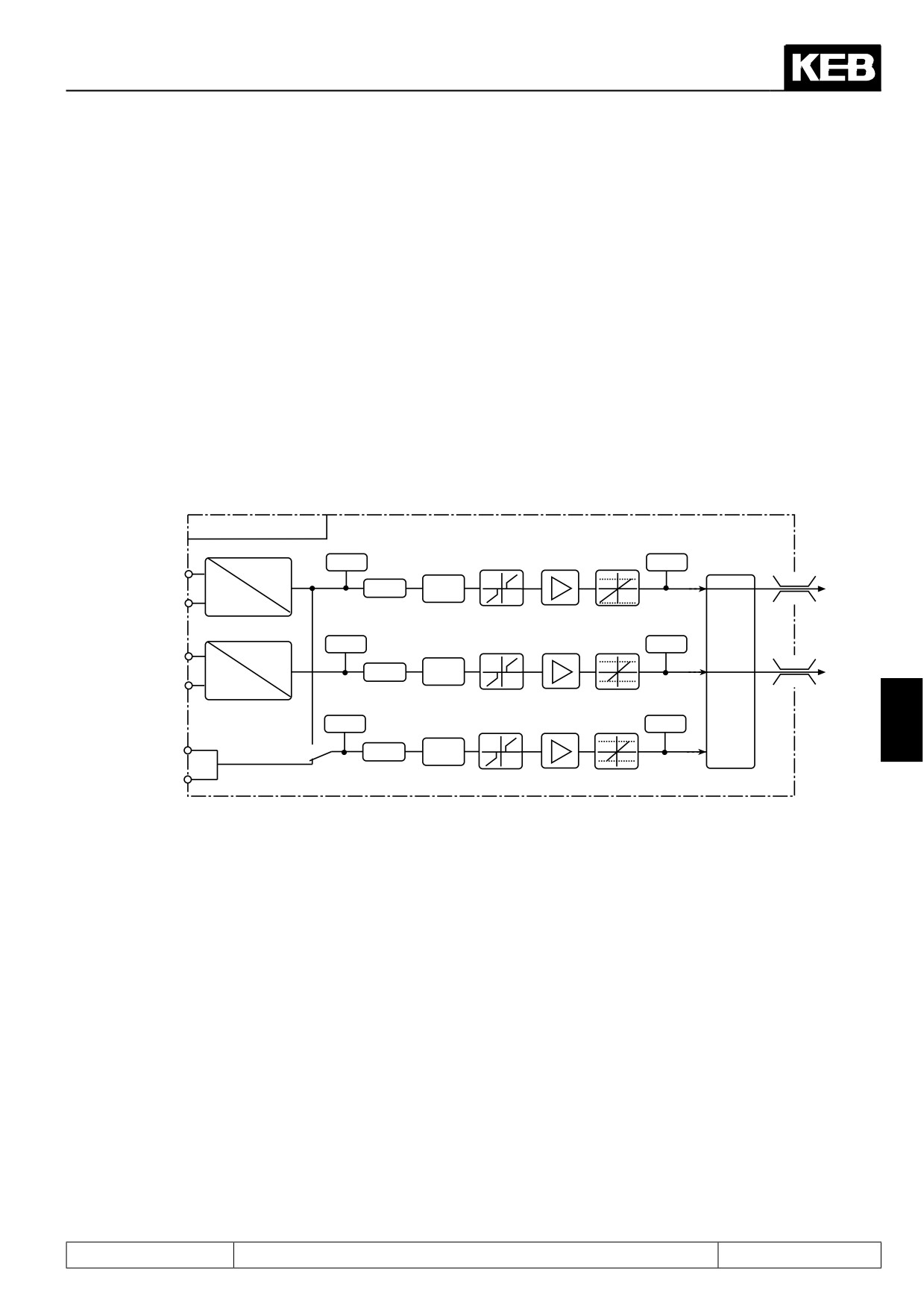
By selecting an input interface (An.00 / 10) input AN1, e.g. AN2 can be adjusted to the applied input signal. By
An.20 the third analog input can be switched additionally to AN1. Subsequently the analog inputs are smoothed
in an electronic filter (An.01 / 11 / 21) by averaging. With An.02 / 12 / 22 a save mode can be adjusted and
activated with a programmable input (An.03 / 13 / 23). To inhibit voltage fluctuations and ripple voltages around
the zero point the analog signal can be faded out around the zero point up to ±10 % (An.04 / 14 / 24). In the
characteristics amplifier the input signals can be influenced in X and Y direction as well as in the rise (An.05...07
/ 15...17 / 25...27). At the output of the characteristic amplifier the signal can be limited to a minimum and a ma-
ximum value (An.08, 09 / 18, 19 / 28, 29). At the output of the block it can be defined with An.30 which analog
signal serves as reference value and which one serves as auxiliary value. The ru-parameters are used for the
indication of the analog signal before and after the amplification. The internal values are limited to ±400%.
Figure 7.2.1 Principle of the analog inputs
Analog Inputs
An.5
An.0
An.6
An.8
ru.27
An.4
An.7
ru.28
0...±100%
An.9
An.30
+AN1 (X2A.1)
An.2
400%
±10V
An.1
0...±20mA
An.3
-400%
REF
-AN1 (X2A.2)
4...20mA
An.15
An.10
An.16
An.18
ru.29
An.14
An.17
An.19
ru.30
0...±100%
+AN2 (X2A.3)
An.12
400%
±10V
An.11
AUX
An.13
-400%
-AN2 (X2A.4)
0...±20mA
4...20mA
An.25
An.26
An.28
ru.31
An.24
An.27
An.29
ru.32
7
An.22
An.21
+AN3 (opt.)
An.23
An.20
-AN3 (opt.)
An.00
AN1 interface selection
An.19
AN2 upper limit
An.01
AN1 noise filter
An.20
AN3 interface selection
An.02
AN1 save mode
An.21
AN3 noise filter
An.03
AN1 save trigger input selection
An.22
AN3 save mode
An.04
AN1 zero clamp
An.23
AN3 save trigger input selection
An.05
AN1 gain
An.24
AN3 zero clamp
An.06
AN1 offset X
An.25
AN3 gain
An.07
AN1 offset Y
An.26
AN3 offset X
An.08
AN1 lower limit
An.27
AN3 offset Y
An.09
AN1 upper limit
An.28
AN3 lower limit
An.10
AN2 interface selection
An.29
AN3 upper limit
An.11
AN2 noise filter
An.30
Selection REF input / AUX-function
An.12
AN2 save mode
An.13
AN2 save trigger input selection
ru.27
AN1 pre amplifier display
An.14
AN2 zero clamp
ru.28
AN1 post amplifier display
An.15
AN2 gain
ru.29
AN2 pre amplifier display
An.16
AN2 offset X
ru.30
AN2 post amplifier display
An.17
AN2 offset Y
ru.31
AN3 pre amplifier display
An.18
AN2 lower limit
ru.32
AN3 post amplifier display
Page7.2 - 3
Analog In- and Outputs I
7.2.2
Interface selection
7.2.2.1AN1 / AN2 (An.00, An.10)
Depending on the selected interface (An.00 /An.10) the analog inputs AN1 and AN2 can process following input
signals:
An.00 / An.10
= 0
0...±10 V (default)
= 1
0...±20 mA
= 2
4...20 mA
Figure 7.2.2.a Connection as differential voltage inputs 0...±10V DC
Ri = 55 kOhm
2
3
4
5
6
7
8
9
PE
X2A. 1
1)
+
-
+
-
SPS
SPS
0...±10 VDC
1) Connect equipotential bonding conductor only, if a potential difference of > 30 V exists between the controls.
The internal resistance is reduced to 30 kOhm.
Figure 7.2.2.b Triggering with poti and internally reference voltage
2
3
4
5
6
7
8
9
PE
X2A. 1
R = 3...10 k
0...10V DC Ri=30kΩ (An.00 / An.10 = 0) The output CRF Terminal X2A.7 may be loaded with maximal 6mA!
Figure 7.2.2.c Triggering with current signal (An.00 / An.10 = 1 or 2)
2
3
4
5
6
7
8
9
PE
X2A. 1
+
+
0...±20 mADC
4...20 mADC
Ri = 250 Ω
Page7.2 - 4
Analog In- and Outputs I
7.2.2.2AN3 (An.20)
With An.20 it is determined from where the 3. analog input value is received. Following values can be defined:
Value
Function
0
Analog option (AN3)
1
Analog input 1 (AN1)
7.2.3
Noise filter (An.01, An.11, An.21)
The noise filters shall suppress disturbances and ripples of the input signals. If the noise filter is switched off the
analog inputs are queried every 1 ms and the recorded value is then transferred. The noise filter adjustments
specify the number of sampled data for averaging.
An.01/ 11/ 21: Interference suppression filter
Value
Function
0
off (no averaging)
1
double
2
4-fold
3
8-fold
4
16-fold
7.2.4
Save mode (An.02, An.12, An.22)
7
Coming from the input filter the save mode can be switched on with An.02 / An.12 / An.22. If now the program-
mable digital input (value 1) is set the analog signal is processed directly and written parallel into the non-
volatile memory. As soon as the digital input is disconnected (value 0), the inverter continuos to run with value
stored in the memory. Moreover, with An.02 / An.12 / An.22 it can be determined whether the memory contents
are saved upon switch off.
An.02/ 12/ 22: Save mode
Bit
Value
Meaning
0
Direct mode (default)
0
1
Save mode
0
Do not delete memory contents at switch off (default)
1
2
Delete memory contents at switch off
Page7.2 - 5