Atmel ATmega328P 8-bit AVR Microcontroller. DATASHEET (2015) - page 7
• Bit 7 - SPMIE: SPM Interrupt Enable
When the SPMIE bit is written to one, and the I-bit in the status register is set (one), the SPM ready interrupt will be enabled.
The SPM ready interrupt will be executed as long as the SELFPRGEN bit in the SPMCSR register is cleared.
• Bit 6 - RWWSB: Read-While-Write Section Busy
When a self-programming (page erase or page write) operation to the RWW section is initiated, the RWWSB will be set
(one) by hardware. When the RWWSB bit is set, the RWW section cannot be accessed. The RWWSB bit will be cleared if
the RWWSRE bit is written to one after a self-programming operation is completed. Alternatively the RWWSB bit will
automatically be cleared if a page load operation is initiated.
• Bit 5 - Res: Reserved Bit
This bit is a reserved bit in the Atmel® ATmega328P and always read as zero.
• Bit 4 - RWWSRE: Read-While-Write Section Read Enable
When programming (page erase or page write) to the RWW section, the RWW section is blocked for reading (the RWWSB
will be set by hardware). To re-enable the RWW section, the user software must wait until the programming is completed
(SELFPRGEN will be cleared). Then, if the RWWSRE bit is written to one at the same time as SELFPRGEN, the next SPM
instruction within four clock cycles re-enables the RWW section. The RWW section cannot be re-enabled while the flash is
busy with a page erase or a page write (SELFPRGEN is set). If the RWWSRE bit is written while the flash is being loaded,
the flash load operation will abort and the data loaded will be lost.
• Bit 3 - BLBSET: Boot Lock Bit Set
If this bit is written to one at the same time as SELFPRGEN, the next SPM instruction within four clock cycles sets boot lock
bits and memory lock bits, according to the data in R0. The data in R1 and the address in the Z-pointer are ignored. The
BLBSET bit will automatically be cleared upon completion of the lock bit set, or if no SPM instruction is executed within four
clock cycles.
An LPM instruction within three cycles after BLBSET and SELFPRGEN are set in the SPMCSR register, will read either the
lock bits or the fuse bits (depending on Z0 in the Z-pointer) into the destination register. See Section 26.8.9 “Reading the
Fuse and Lock Bits from Software” on page 235 for details.
• Bit 2 - PGWRT: Page Write
If this bit is written to one at the same time as SELFPRGEN, the next SPM instruction within four clock cycles executes page
write, with the data stored in the temporary buffer. The page address is taken from the high part of the Z-pointer. The data in
R1 and R0 are ignored. The PGWRT bit will auto-clear upon completion of a page write, or if no SPM instruction is executed
within four clock cycles. The CPU is halted during the entire page write operation if the NRWW section is addressed.
• Bit 1 - PGERS: Page Erase
If this bit is written to one at the same time as SELFPRGEN, the next SPM instruction within four clock cycles executes page
erase. The page address is taken from the high part of the Z-pointer. The data in R1 and R0 are ignored. The PGERS bit will
auto-clear upon completion of a page erase, or if no SPM instruction is executed within four clock cycles. The CPU is halted
during the entire page write operation if the NRWW section is addressed.
• Bit 0 - SELFPRGEN: Self Programming Enable
This bit enables the SPM instruction for the next four clock cycles. If written to one together with either RWWSRE, BLBSET,
PGWRT or PGERS, the following SPM instruction will have a special meaning, see description above. If only SELFPRGEN
is written, the following SPM instruction will store the value in R1:R0 in the temporary page buffer addressed by the
Z-pointer. The LSB of the Z-pointer is ignored. The SELFPRGEN bit will auto-clear upon completion of an SPM instruction,
or if no SPM instruction is executed within four clock cycles. During page erase and page write, the SELFPRGEN bit remains
high until the operation is completed.
Writing any other combination than “10001”, “01001”, “00101”, “00011” or “00001” in the lower five bits will have no effect.
240
ATmega328P [DATASHEET]
7810D-AVR-01/15
27.
Memory Programming
27.1
Program And Data Memory Lock Bits
The Atmel® ATmega328P provides six lock bits which can be left unprogrammed (“1”) or can be programmed (“0”) to obtain
the additional features listed in Table 27-2. The lock bits can only be erased to “1” with the chip erase command.The
ATmega328P has no separate boot loader section. The SPM instruction is enabled for the whole flash if the SELFPRGEN
fuse is programmed (“0”), otherwise it is disabled.
Table 27-1. Lock Bit Byte(1)
Lock Bit Byte
Bit No
Description
Default Value
7
-
1 (unprogrammed)
6
-
1 (unprogrammed)
BLB12(2)
5
Boot lock bit
1 (unprogrammed)
BLB11(2)
4
Boot lock bit
1 (unprogrammed)
BLB02(2)
3
Boot lock bit
1 (unprogrammed)
BLB01(2)
2
Boot lock bit
1 (unprogrammed)
LB2
1
Lock bit
1 (unprogrammed)
LB1
0
Lock bit
1 (unprogrammed)
Notes:
1.
“1” means unprogrammed, “0” means programmed
2.
Only on ATmega328P.
Table 27-2. Lock Bit Protection Modes(1)(2)
Memory Lock Bits
Protection Type
LB Mode
LB2
LB1
1
1
1
No memory lock features enabled.
Further programming of the flash and EEPROM is disabled in parallel and
2
1
0
serial programming mode. The fuse bits are locked in both serial and parallel
programming mode.(1)
Further programming and verification of the flash and EEPROM is disabled in
3
0
0
parallel and serial programming mode. The boot lock bits and fuse bits are
locked in both serial and parallel programming mode.(1)
Notes:
1.
Program the fuse bits and boot lock bits before programming the LB1 and LB2.
2.
“1” means unprogrammed, “0” means programmed
ATmega328P [DATASHEET]
241
7810D-AVR-01/15

Table 27-3. Lock Bit Protection Modes(1)(2)
BLB0 Mode
BLB02
BLB01
1
1
1
No restrictions for SPM or LPM accessing the application section.
2
1
0
SPM is not allowed to write to the application section.
SPM is not allowed to write to the application section, and LPM executing
from the boot loader section is not allowed to read from the application
3
0
0
section. If interrupt vectors are placed in the boot loader section, interrupts
are disabled while executing from the application section.
LPM executing from the boot loader section is not allowed to read from the
4
0
1
application section. If interrupt vectors are placed in the boot loader section,
interrupts are disabled while executing from the application section.
BLB1 Mode
BLB12
BLB11
1
1
1
No restrictions for SPM or LPM accessing the boot loader section.
2
1
0
SPM is not allowed to write to the boot loader section.
SPM is not allowed to write to the boot loader section, and LPM executing
from the application section is not allowed to read from the boot loader
3
0
0
section. If interrupt vectors are placed in the application section, interrupts
are disabled while executing from the boot loader section.
LPM executing from the application section is not allowed to read from the
4
0
1
boot loader section. If interrupt vectors are placed in the application section,
interrupts are disabled while executing from the boot loader section.
Notes:
1.
Program the fuse bits and boot lock bits before programming the LB1 and LB2.
2.
“1” means unprogrammed, “0” means programmed
27.2
Fuse Bits
The ATmega328P has three fuse bytes. Table 27-4 - Table 27-7 on page 244 describe briefly the functionality of all the fuses
and how they are mapped into the fuse bytes. Note that the fuses are read as logical zero, “0”, if they are programmed.
Table 27-4. Extended Fuse Byte for ATmega328P
Extended Fuse Byte
Bit No
Description
Default Value
–
7
-
1
–
6
-
1
–
5
-
1
–
4
-
1
–
3
-
1
–
2
-
1
–
1
-
1
SELFPRGEN
0
Self programming enable
1 (unprogrammed)
242
ATmega328P [DATASHEET]
7810D-AVR-01/15

Table 27-5. Extended Fuse Byte for ATmega328P
Extended Fuse Byte
Bit No.
Description
Default Value
–
7
-
1
–
6
-
1
–
5
-
1
–
4
-
1
–
3
-
1
BODLEVEL2(1)
2
Brown-out detector trigger level
1 (unprogrammed)
BODLEVEL1(1)
1
Brown-out detector trigger level
1 (unprogrammed)
BODLEVEL0(1)
0
Brown-out detector trigger level
1 (unprogrammed)
Note:
1.
See Table 28-5 on page 262 for BODLEVEL fuse decoding.
Table 27-6. Fuse High Byte for ATmega328P
High Fuse Byte
Bit No.
Description
Default Value
RSTDISBL(1)
7
External reset disable
1 (unprogrammed)
DWEN
6
debugWIRE enable
1 (unprogrammed)
Enable serial program and data
0 (programmed, SPI programming
SPIEN(2)
5
downloading
enabled)
WDTON(3)
4
Watchdog timer always On
1 (unprogrammed)
EEPROM memory is preserved
1 (unprogrammed), EEPROM not
EESAVE
3
through the chip erase
reserved
Select boot size
BOOTSZ1
2
(see Table 26-7 on page 239
0 (programmed)(4)
for details)
Select boot size
BOOTSZ0
1
(see Table 26-7 on page 239
0 (programmed)(4)
for details)
BOOTRST
0
Select reset vector
1 (unprogrammed)
Notes:
1.
See Section 13.3.2 “Alternate Functions of Port C” on page 68 for description of RSTDISBL fuse.
2.
The SPIEN fuse is not accessible in serial programming mode.
3.
See Section 10.9.2 “WDTCSR - Watchdog Timer Control Register” on page 47 for details.
4.
The default value of BOOTSZ[1:0] results in maximum boot size. See Section 27-11 “Pin Name Mapping” on
page 246.
ATmega328P [DATASHEET]
243
7810D-AVR-01/15

Table 27-7. Fuse Low Byte
Low Fuse Byte
Bit No.
Description
Default Value
CKDIV8(2)4
7
Divide clock by 8
0 (programmed)
CKOUT(3)
6
Clock output
1 (unprogrammed)
SUT1
5
Select start-up time
1 (unprogrammed)(1)
SUT0
4
Select start-up time
0 (programmed)(1)
CKSEL3
3
Select clock source
0 (programmed)(2)
CKSEL2
2
Select clock source
0 (programmed)(2)
CKSEL1
1
Select clock source
1 (unprogrammed)(2)
CKSEL0
0
Select clock source
0 (programmed)
Notes:
1.
The default value of SUT1..0 results in maximum start-up time for the default clock source. See Table 8-11 on
page 30 for details.
2.
The default setting of CKSEL3..0 results in internal RC oscillator at 8MHz. See Table 8-10 on page 30 for
details.
3.
The CKOUT fuse allows the system clock to be output on PORTB0. See Section 8.9 “Clock Output Buffer” on
page 31 for details.
4.
See Section 8.11 “System Clock Prescaler” on page 32 for details.
The status of the fuse bits is not affected by chip erase. Note that the fuse bits are locked if lock bit1 (LB1) is programmed.
program the fuse bits before programming the lock bits.
27.2.1
Latching of Fuses
The fuse values are latched when the device enters programming mode and changes of the fuse values will have no effect
until the part leaves programming mode. This does not apply to the EESAVE fuse which will take effect once it is
programmed. The fuses are also latched on power-up in normal mode.
27.3
Signature Bytes
All Atmel microcontrollers have a three-byte signature code which identifies the device. This code can be read in both serial
and parallel mode, also when the device is locked. The three bytes reside in a separate address space. For the Atmel®
ATmega328P the signature bytes are given in Table 27-8.
Table 27-8. Device ID
Signature Bytes Address
Part
0x000
0x001
0x002
ATmega328P
0x1E
0x95
0x0F
27.4
Calibration Byte
The Atmel ATmega328P has a byte calibration value for the internal RC oscillator. This byte resides in the high byte of
address 0x000 in the signature address space. During reset, this byte is automatically written into the OSCCAL register to
ensure correct frequency of the calibrated RC oscillator.
244
ATmega328P [DATASHEET]
7810D-AVR-01/15
27.5
Page Size
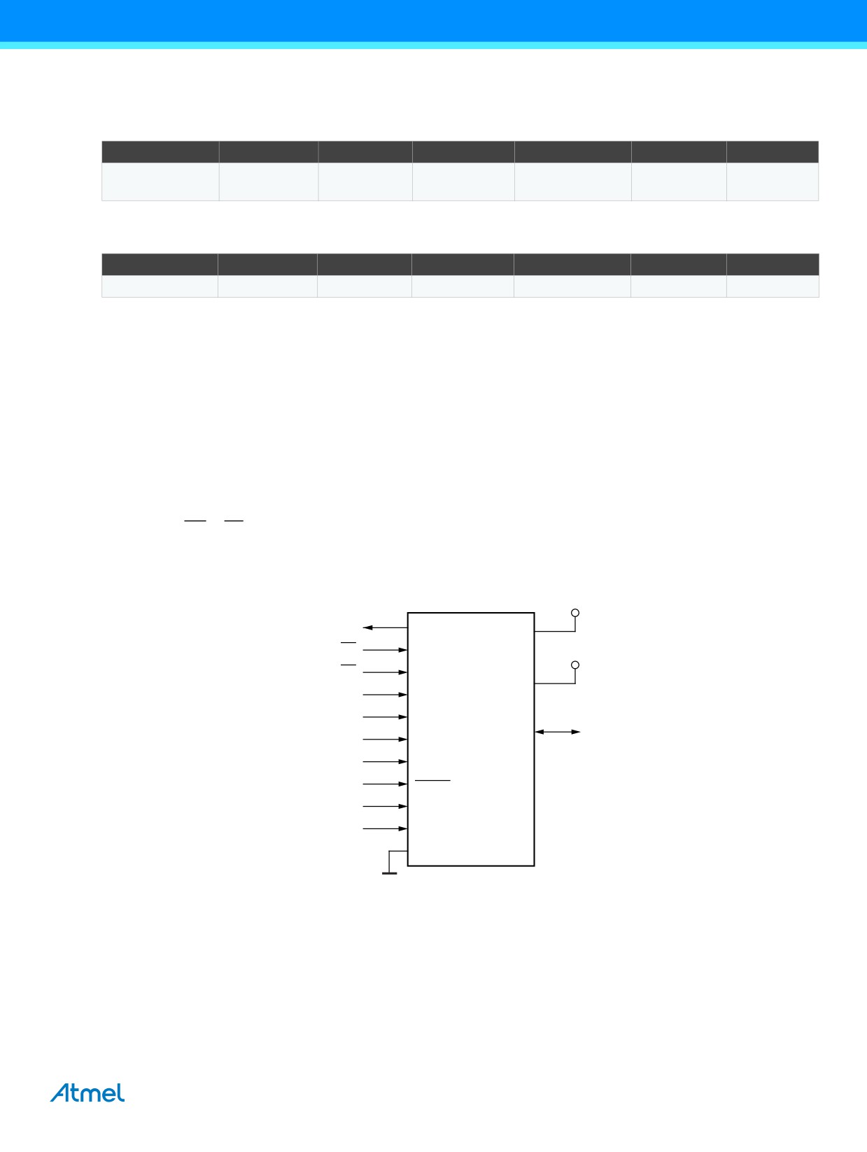
Table 27-9. No. of Words in a Page and No. of Pages in the Flash
Device
Flash Size
Page Size
PCWORD
No. of Pages
PCPAGE
PCMSB
16K words
ATmega328P
64 words
PC[5:0]
256
PC[13:6]
13
(32K bytes)
Table 27-10. No. of Words in a Page and No. of Pages in the EEPROM
Device
EEPROM Size
Page Size
PCWORD
No. of Pages
PCPAGE
EEAMSB
ATmega328P
1K bytes
4 bytes
EEA[1:0]
256
EEA[9:2]
9
27.6
Parallel Programming Parameters, Pin Mapping, and Commands
This section describes how to parallel program and verify flash program memory, EEPROM data memory, memory lock bits,
and fuse bits in the ATmega328P. Pulses are assumed to be at least 250ns unless otherwise noted.
27.6.1
Signal Names
In this section, some pins of the Atmel® ATmega328P are referenced by signal names describing their functionality during
parallel programming, see Figure 27-1 and Table 27-11 on page 246. Pins not described in the following table are referenced
by pin names.
The XA1/XA0 pins determine the action executed when the XTAL1 pin is given a positive pulse. The bit coding is shown in
Table 27-13 on page 246.
When pulsing WR or OE, the command loaded determines the action executed. The different commands are shown in Table
27-14 on page 246.
Figure 27-1. Parallel Programming
+ 4.5V to 5.5V
RDY/BSY
PD1
VCC
OE
PD2
+ 4.5V to 5.5V
WR
PD3
AVCC
BS1
PD4
XA0
PD5
PC[1:0]:PB[5:0]
DATA
XA1
PD6
PAGEL
PD7
+12V
RESET
BS2
PC2
XTAL1
GND
Note:
VCC to 0.3V < AVCC < VCC + 0.3V, however, AVCC should always be within 4.5 to 5.5V
ATmega328P [DATASHEET]
245
7810D-AVR-01/15
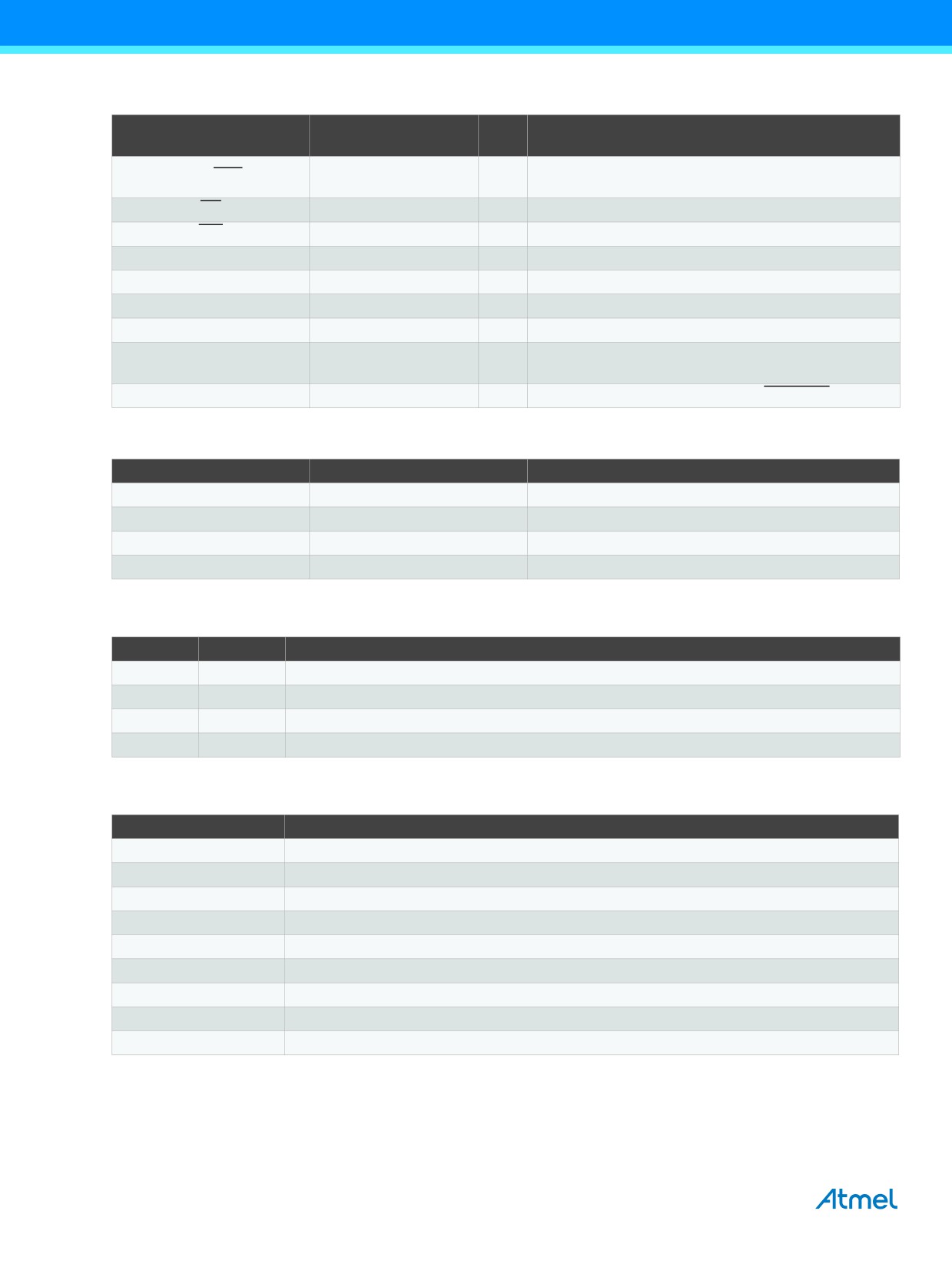
Table 27-11. Pin Name Mapping
Signal Name in
Programming Mode
Pin Name
I/O
Function
0: Device is busy programming, 1: Device is ready for
RDY/BSY
PD1
O
new command
OE
PD2
I
Output enable (active low)
WR
PD3
I
Write pulse (active low)
BS1
PD4
I
Byte select 1 (“0” selects low byte, “1” selects high byte)
XA0
PD5
I
XTAL action Bit 0
XA1
PD6
I
XTAL action Bit 1
PAGEL
PD7
I
Program memory and EEPROM data page load
Byte select 2 (“0” selects low byte, “1” selects 2’nd high
BS2
PC2
I
byte)
DATA
{PC[1:0]: PB[5:0]}
I/O
Bi-directional data bus (output when OE is low)
Table 27-12. Pin Values Used to Enter Programming Mode
Pin
Symbol
Value
PAGEL
Prog_enable[3]
0
XA1
Prog_enable[2]
0
XA0
Prog_enable[1]
0
BS1
Prog_enable[0]
0
Table 27-13. XA1 and XA0 Coding
XA1
XA0
Action when XTAL1 is Pulsed
0
0
Load flash or EEPROM address (high or low address byte determined by BS1).
0
1
Load data (high or low data byte for flash determined by BS1).
1
0
Load command
1
1
No action, idle
Table 27-14. Command Byte Bit Coding
Command Byte
Command Executed
1000 0000
Chip erase
0100 0000
Write fuse bits
0010 0000
Write lock bits
0001 0000
Write flash
0001 0001
Write EEPROM
0000 1000
Read signature bytes and calibration byte
0000 0100
Read fuse and lock bits
0000 0010
Read flash
0000 0011
Read EEPROM
246
ATmega328P [DATASHEET]
7810D-AVR-01/15
27.7
Parallel Programming
27.7.1
Enter Programming Mode
The following algorithm puts the device in parallel (high-voltage) programming mode:
1.
Set prog_enable pins listed in Table 27-12 on page 246 to “0000”, RESET pin to 0V and VCC to 0V.
2.
Apply 4.5 to 5.5V between VCC and GND.
Ensure that VCC reaches at least àpçV within the next 20µs.
3.
Wait 20 to 60µs, and apply 11.5 to 12.5V to RESET.
4.
Keep the Prog_enable pins unchanged for at least10µs after the high-voltage has been applied to ensure the
prog_enable signature has been latched.
5.
Wait at least 300µs before giving any parallel programming commands.
6.
Exit programming mode by power the device down or by bringing RESET pin to 0V.
If the rise time of the VCC is unable to fulfill the requirements listed above, the following alternative algorithm can be used.
1.
Set prog_enable pins listed in Table 27-12 on page 246 to “0000”, RESET pin to 0V and VCC to 0V.
2.
Apply 4.5 to 5.5V between VCC and GND.
3.
Monitor VCC, and as soon as VCC reaches 0.9 to 1.1V, apply 11.5 to 12.5V to RESET.
4.
Keep the prog_enable pins unchanged for at least 10µs after the high-voltage has been applied to ensure the
prog_enable signature has been latched.
5.
Wait until VCC actually reaches 4.5 to 5.5V before giving any parallel programming commands.
6.
Exit programming mode by power the device down or by bringing RESET pin to 0V.
27.7.2
Considerations for Efficient Programming
The loaded command and address are retained in the device during programming. For efficient programming, the following
should be considered.
● The command needs only be loaded once when writing or reading multiple memory locations.
● Skip writing the data value 0xFF, that is the contents of the entire EEPROM (unless the EESAVE fuse is programmed)
and flash after a chip erase.
● Address high byte needs only be loaded before programming or reading a new 256 word window in flash or 256 byte
EEPROM. This consideration also applies to signature bytes reading.
27.7.3
Chip Erase
The chip erase will erase the flash and EEPROM(1) memories plus lock bits. The lock bits are not reset until the program
memory has been completely erased. The fuse bits are not changed. A chip erase must be performed before the flash
and/or EEPROM are reprogrammed.
Note:
1.
The EEPRPOM memory is preserved during chip erase if the EESAVE fuse is programmed.
Load command “chip erase”
1.
Set XA1, XA0 to “10”. This enables command loading.
2.
Set BS1 to “0”.
3.
Set DATA to “1000 0000”. This is the command for chip erase.
4.
Give XTAL1 a positive pulse. This loads the command.
5.
Give WR a negative pulse. This starts the chip erase. RDY/BSY goes low.
6.
Wait until RDY/BSY goes high before loading a new command.
ATmega328P [DATASHEET]
247
7810D-AVR-01/15
27.7.4
Programming the Flash
The Flash is organized in pages, see Table 27-9 on page 245. When programming the flash, the program data is latched into
a page buffer. This allows one page of program data to be programmed simultaneously. The following procedure describes
how to program the entire flash memory:
A. Load Command “Write Flash”
1.
Set XA1, XA0 to “10”. This enables command loading.
2.
Set BS1 to “0”.
3.
Set DATA to “0001 0000”. This is the command for write flash.
4.
Give XTAL1 a positive pulse. This loads the command.
B. Load Address Low byte
1.
Set XA1, XA0 to “00”. This enables address loading.
2.
Set BS1 to “0”. This selects low address.
3.
Set DATA = Address low byte (0x00 - 0xFF).
4.
Give XTAL1 a positive pulse. This loads the address low byte.
C. Load Data Low Byte
1.
Set XA1, XA0 to “01”. This enables data loading.
2.
Set DATA = Data low byte (0x00 - 0xFF).
3.
Give XTAL1 a positive pulse. This loads the data byte.
D. Load Data High Byte
1.
Set BS1 to “1”. This selects high data byte.
2.
Set XA1, XA0 to “01”. This enables data loading.
3.
Set DATA = Data high byte (0x00 - 0xFF).
4.
Give XTAL1 a positive pulse. This loads the data byte.
E. Latch Data
1.
Set BS1 to “1”. This selects high data byte.
2.
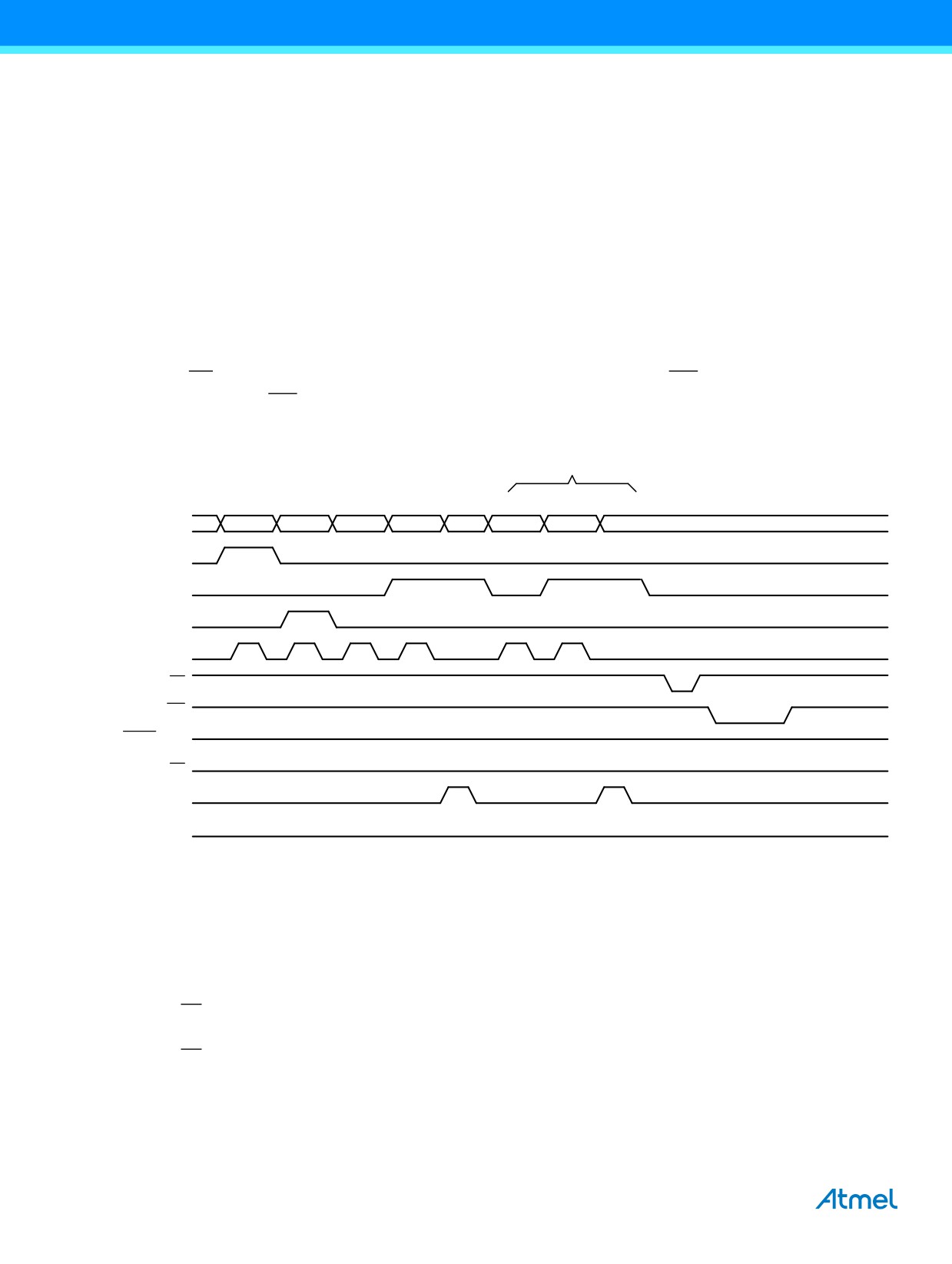
Give PAGEL a positive pulse. This latches the data bytes. (See Figure 27-3 on page 249 for signal waveforms)
F. Repeat B through E until the entire buffer is filled or until all data within the page is loaded.
While the lower bits in the address are mapped to words within the page, the higher bits address the pages within the flash.
This is illustrated in Figure 27-2 on page 249. Note that if less than eight bits are required to address words in the page
(Page size < 256), the most significant bit(s) in the address low byte are used to address the page when performing a page
write.
G. Load Address High byte
1.
Set XA1, XA0 to “00”. This enables address loading.
2.
Set BS1 to “1”. This selects high address.
3.
Set DATA = Address high byte (0x00 - 0xFF).
4.
Give XTAL1 a positive pulse. This loads the address high byte.
H. Program Page
1.
Give WR a negative pulse. This starts programming of the entire page of data. RDY/BSY goes low.
2.
Wait until RDY/BSY goes high (See Figure 27-3 on page 249 for signal waveforms).
I. Repeat B through H until the entire flash is programmed or until all data has been programmed.
J. End page programming
1.
1. Set XA1, XA0 to “10”. This enables command loading.
2.
Set DATA to “0000 0000”. This is the command for No operation.
3.
Give XTAL1 a positive pulse. This loads the command, and the internal write signals are reset.
248
ATmega328P [DATASHEET]
7810D-AVR-01/15
Figure 27-2. Addressing the Flash which is Organized in Pages(1)
PCMSB
PAGEMSB
Program
Counter
PCPAGE
PCWORD
Page Address
Word Address
within the Flash
within a Page
Program Memory
Page
PCWORD[PAGEMSB:0]
Page
Instruction Word
00
01
02
PAGEEND
Note:
1.
PCPAGE and PCWORD are listed in Table 27-9 on page 245.
Figure 27-3. Programming the Flash Waveforms(1)
F
A
B
C
D
E
B
C
D
E
G
H
DATA
0x10
ADDR. LOW
DATA LOW DATA HIGH
XX
ADDR. LOW DATA LOW DATA HIGH
XX
ADDR. HIGH
XX
XA1
XA0
BS1
XTAL1
WR
RDY/BSY
RESET +12V
OE
PAGEL
BS2
Note:
1.
“XX” is don’t care. The letters refer to the programming description above.
ATmega328P [DATASHEET]
249
7810D-AVR-01/15
27.7.5
Programming the EEPROM
The EEPROM is organized in pages, see Table 27-10 on page 245. When programming the EEPROM, the program data is
latched into a page buffer. This allows one page of data to be programmed simultaneously. The programming algorithm for
the EEPROM data memory is as follows (refer to Section 27.7.4 “Programming the Flash” on page 248 for details on
command, address and data loading):
1.
A: Load Command “0001 0001”.
2.
G: Load Address High Byte (0x00 - 0xFF).
3.
B: Load Address Low Byte (0x00 - 0xFF).
4.
C: Load Data (0x00 - 0xFF).
5.
E: Latch data (give PAGEL a positive pulse).
K: Repeat 3 through 5 until the entire buffer is filled.
L: Program EEPROM page
1.
Set BS1 to “0”.
2.
Give WR a negative pulse. This starts programming of the EEPROM page. RDY/BSY goes low.
3.
Wait until to RDY/BSY goes high before programming the next page (See Figure 27-4 for signal waveforms).
Figure 27-4. Programming the EEPROM Waveforms
K
A
G
B
C
E
B
C
E
L
DATA
0x11
ADDR. HIGH
ADDR. LOW
DATA
XX
ADDR. LOW
DATA
XX
XA1
XA0
BS1
XTAL1
WR
RDY/BSY
RESET +12V
OE
PAGEL
BS2
27.7.6
Reading the Flash
The algorithm for reading the flash memory is as follows (refer to Section 27.7.4 “Programming the Flash” on page 248 for
details on command and address loading):
1.
A: Load command “0000 0010”.
2.
G: Load address high byte (0x00 - 0xFF).
3.
B: Load address low byte (0x00 - 0xFF).
4.
Set OE to “0”, and BS1 to “0”. The flash word low byte can now be read at DATA.
5.
Set BS1 to “1”. The flash word high byte can now be read at DATA.
6.
Set OE to “1”.
250
ATmega328P [DATASHEET]
7810D-AVR-01/15
27.7.7
Reading the EEPROM
The algorithm for reading the EEPROM memory is as follows (refer to Section 27.7.4 “Programming the Flash” on page 248
for details on command and address loading):
1.
A: Load command “0000 0011”.
2.
G: Load address high byte (0x00 - 0xFF).
3.
B: Load address low byte (0x00 - 0xFF).
4.
Set OE to “0”, and BS1 to “0”. The EEPROM data byte can now be read at DATA.
5.
Set OE to “1”.
27.7.8
Programming the Fuse Low Bits
The algorithm for programming the fuse low bits is as follows (refer to Section 27.7.4 “Programming the Flash” on page 248
for details on command and data loading):
1.
A: Load command “0100 0000”.
2.
C: Load data low byte. Bit n = “0” programs and bit n = “1” erases the fuse bit.
3.
Give WR a negative pulse and wait for RDY/BSY to go high.
27.7.9
Programming the Fuse High Bits
The algorithm for programming the fuse high bits is as follows (refer to Section 27.7.4 “Programming the Flash” on page 248
for details on command and data loading):
1.
A: Load command “0100 0000”.
2.
C: Load data low byte. Bit n = “0” programs and bit n = “1” erases the fuse bit.
3.
Set BS1 to “1” and BS2 to “0”. This selects high data byte.
4.
Give WR a negative pulse and wait for RDY/BSY to go high.
5.
Set BS1 to “0”. This selects low data byte.
27.7.10 Programming the Extended Fuse Bits
The algorithm for programming the extended fuse bits is as follows (refer to Section 27.7.4 “Programming the Flash” on page
248 for details on command and data loading):
1.
1. A: Load command “0100 0000”.
2.
2. C: Load data low byte. Bit n = “0” programs and bit n = “1” erases the fuse bit.
3.
3. Set BS1 to “0” and BS2 to “1”. This selects extended data byte.
4.
4. Give WR a negative pulse and wait for RDY/BSY to go high.
5.
5. Set BS2 to “0”. This selects low data byte.
ATmega328P [DATASHEET]
251
7810D-AVR-01/15
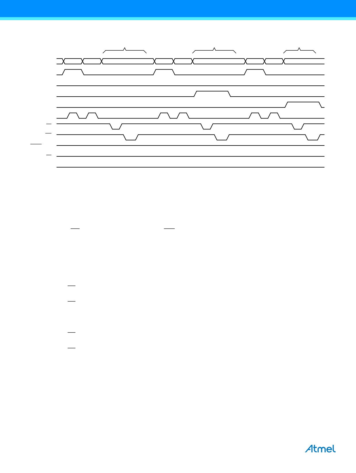
Figure 27-5. Programming the FUSES Waveforms
Write Fuse Low byte
Write Fuse High byte
Write Extended Fuse byte
A
C
A
C
A
C
DATA
0x40
DATA
XX
0x40
DATA
XX
0x40
DATA
XX
XA1
XA0
BS1
BS2
XTAL1
WR
RDY/BSY
RESET +12V
OE
PAGEL
27.7.11 Programming the Lock Bits
The algorithm for programming the lock bits is as follows (refer to Section 27.7.4 “Programming the Flash” on page 248 for
details on command and data loading):
1.
A: Load command “0010 0000”.
2.
C: Load data low byte. Bit n = “0” programs the lock bit. If LB mode 3 is programmed (LB1 and LB2 is
programmed), it is not possible to program the boot lock bits by any external programming mode.
3.
Give WR a negative pulse and wait for RDY/BSY to go high.
The lock bits can only be cleared by executing chip erase.
27.7.12 Reading the Fuse and Lock Bits
The algorithm for reading the fuse and lock bits is as follows (refer to Section 27.7.4 “Programming the Flash” on page 248
for details on command loading):
1.
A: Load command “0000 0100”.
2.
Set OE to “0”, BS2 to “0” and BS1 to “0”. The status of the fuse low bits can now be read at DATA (“0” means
programmed).
3.
Set OE to “0”, BS2 to “1” and BS1 to “1”. The status of the fuse high bits can now be read at DATA (“0” means
programmed).
4.
Set OE to “0”, BS2 to “1”, and BS1 to “0”. The status of the extended fuse bits can now be read at DATA (“0”
means programmed).
5.
Set OE to “0”, BS2 to “0” and BS1 to “1”. The status of the lock bits can now be read at DATA (“0” means
programmed).
6.
Set OE to “1”.
252
ATmega328P [DATASHEET]
7810D-AVR-01/15
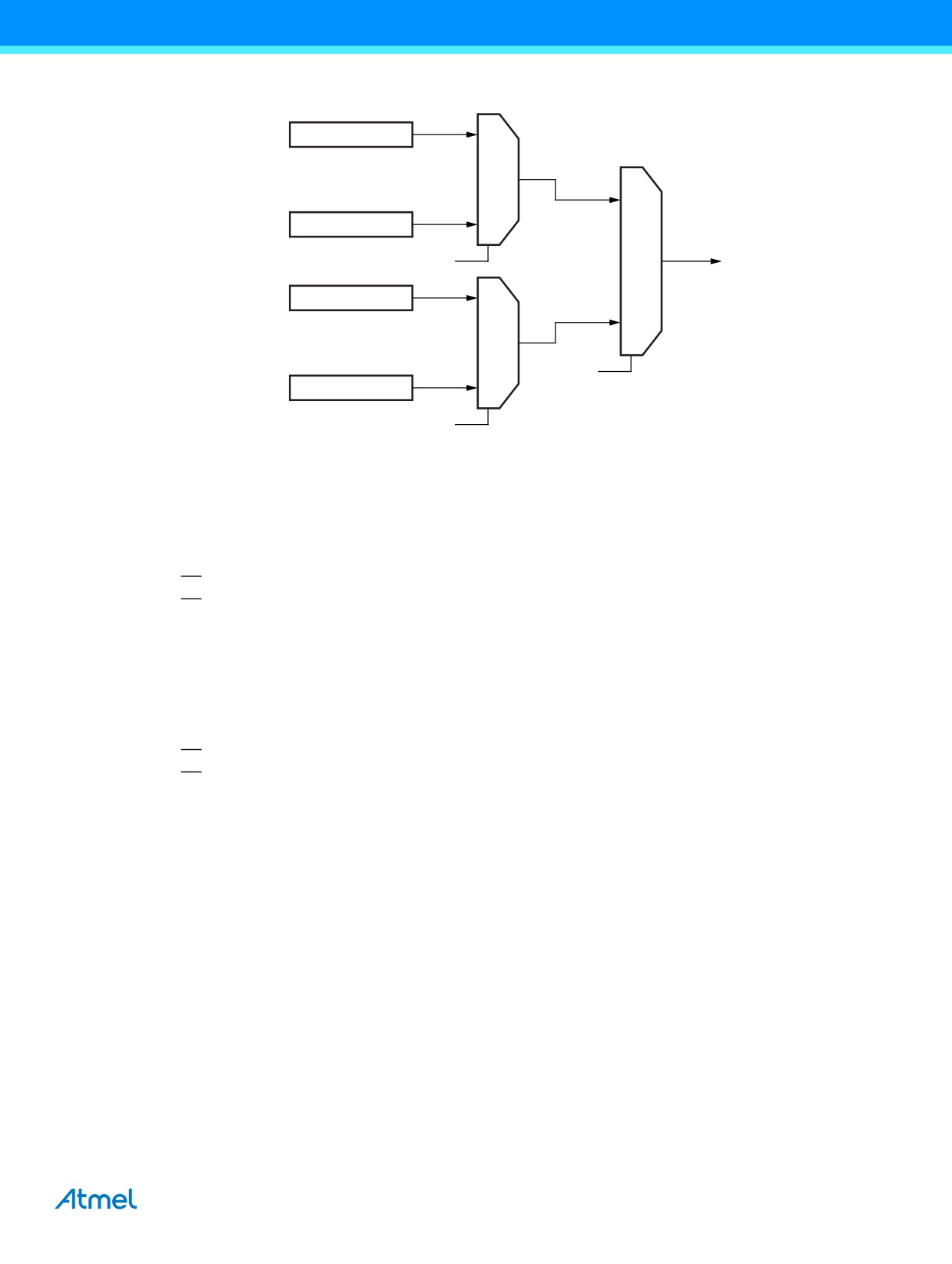
Figure 27-6. Mapping between BS1, BS2 and the Fuse and Lock Bits During Read
Fuse Low Byte
0
0
Extended Fuse Byte
1
DATA
BS2
Lock Bits
0
1
BS1
Fuse High Byte
1
BS2
27.7.13 Reading the Signature Bytes
The algorithm for reading the signature bytes is as follows (refer to Section 27.7.4 “Programming the Flash” on page 248 for
details on command and address loading):
1.
A: Load command “0000 1000”.
2.
B: Load address low byte (0x00 - 0x02).
3.
Set OE to “0”, and BS1 to “0”. The selected signature byte can now be read at DATA.
4.
Set OE to “1”.
27.7.14 Reading the Calibration Byte
The algorithm for reading the calibration byte is as follows (refer to Section 27.7.4 “Programming the Flash” on page 248 for
details on command and address loading):
1.
A: Load command “0000 1000”.
2.
B: Load address low byte, 0x00.
3.
Set OE to “0”, and BS1 to “1”. The calibration byte can now be read at DATA.
4.
Set OE to “1”.
27.7.15 Parallel Programming Characteristics
For characteristics of the parallel programming, see Section 28.10 “Parallel Programming Characteristics” on page 265.
ATmega328P [DATASHEET]
253
7810D-AVR-01/15
27.8
Serial Downloading
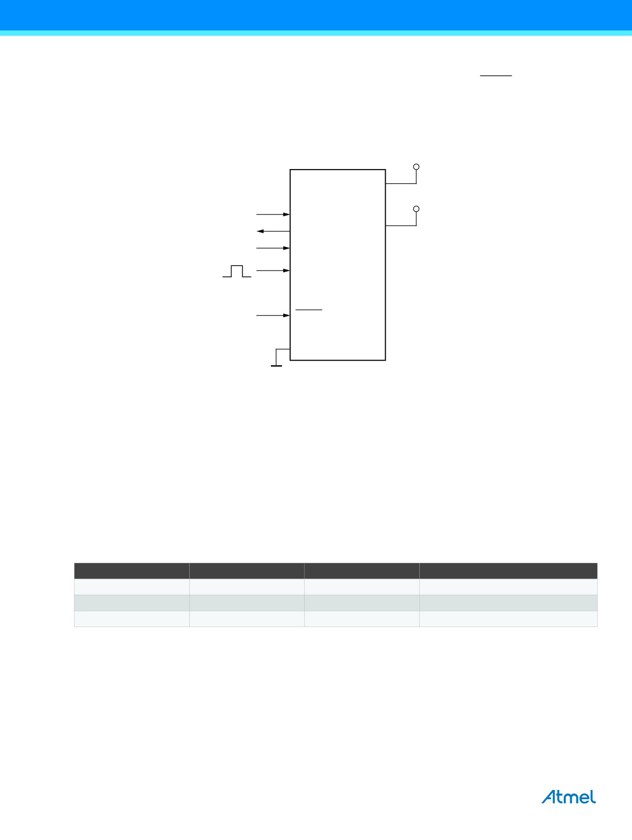
Both the flash and EEPROM memory arrays can be programmed using the serial SPI bus while RESET is pulled to GND.
The serial interface consists of pins SCK, MOSI (input) and MISO (output). After RESET is set low, the programming enable
instruction needs to be executed first before program/erase operations can be executed. NOTE, in Table 27-15, the pin
mapping for SPI programming is listed. Not all parts use the SPI pins dedicated for the internal SPI interface.
Figure 27-7. Serial Programming and Verify(1)
+ 1.8V to 5.5V
VCC
+ 1.8V to 5.5V(2)
MOSI
AVCC
MISO
SCK
XTAL1
RESET
GND
Notes:
1.
If the device is clocked by the internal oscillator, it is no need to connect a clock source to the XTAL1 pin.
2.
VCC - 0.3V < AVCC < VCC + 0.3V, however, AVCC should always be within 2.7 to 5.5V
When programming the EEPROM, an auto-erase cycle is built into the self-timed programming operation (in the serial mode
ONLY) and there is no need to first execute the chip erase instruction. The chip erase operation turns the content of every
memory location in both the program and EEPROM arrays into 0xFF.
Depending on CKSEL fuses, a valid clock must be present. The minimum low and high periods for the serial clock (SCK)
input are defined as follows:
Low:
> 2 CPU clock cycles for fck < 12MHz, 3 CPU clock cycles for fck ≥ 12MHz
High:
> 2 CPU clock cycles for fck < 12MHz, 3 CPU clock cycles for fck ≥ 12MHz
27.8.1
Serial Programming Pin Mapping
Table 27-15. Pin Mapping Serial Programming
Symbol
Pins
I/O
Description
MOSI
PB3
I
Serial data in
MISO
PB4
O
Serial data out
SCK
PB5
I
Serial clock
254
ATmega328P [DATASHEET]
7810D-AVR-01/15
27.8.2
Serial Programming Algorithm
When writing serial data to the Atmel® ATmega328P, data is clocked on the rising edge of SCK.
When reading data from the ATmega328P, data is clocked on the falling edge of SCK. See Figure 27-9 on page 257 for
timing details.
To program and verify the ATmega328P in the serial programming mode, the following sequence is recommended (see
serial programming instruction set in Table 27-17 on page 256):
1.
Power-up sequence:
Apply power between VCC and GND while RESET and SCK are set to “0”. In some systems, the programmer can
not guarantee that SCK is held low during power-up. In this case, RESET must be given a positive pulse of at
least two CPU clock cycles duration after SCK has been set to “0”.
2.
Wait for at least 20ms and enable serial programming by sending the programming enable serial instruction to pin
MOSI.
3.
The serial programming instructions will not work if the communication is out of synchronization. When in sync.
the second byte (0x53), will echo back when issuing the third byte of the programming enable instruction. Whether
the echo is correct or not, all four bytes of the instruction must be transmitted. If the 0x53 did not echo back, give
RESET a positive pulse and issue a new programming enable command.
4.
The flash is programmed one page at a time. The memory page is loaded one byte at a time by supplying the 6
LSB of the address and data together with the load program memory page instruction. To ensure correct loading
of the page, the data low byte must be loaded before data high byte is applied for a given address. The program
memory page is stored by loading the write program memory page instruction with the 7 MSB of the address. If
polling (RDY/BSY) is not used, the user must wait at least tWD_FLASH before issuing the next page (see
Table 27-16). Accessing the serial programming interface before the flash write operation completes can result in
incorrect programming.
5.
A: The EEPROM array is programmed one byte at a time by supplying the address and data together with the
appropriate Write instruction. An EEPROM memory location is first automatically erased before new data is
written. If polling (RDY/BSY) is not used, the user must wait at least tWD_EEPROM before issuing the next byte (see
Table 27-16). In a chip erased device, no 0xFFs in the data file(s) need to be programmed.
B: The EEPROM array is programmed one page at a time. The memory page is loaded one byte at a time by
supplying the 6 LSB of the address and data together with the Load EEPROM memory page instruction. The
EEPROM memory page is stored by loading the write EEPROM memory page instruction with the 7 MSB of the
address. When using EEPROM page access only byte locations loaded with the Load EEPROM memory page
instruction is altered. The remaining locations remain unchanged.
If polling (RDY/BSY) is not used, the used must wait at least tWD_EEPROM before issuing the next byte (see
Table 27-16). In a chip erased device, no 0xFF in the data file(s) need to be programmed.
6.
Any memory location can be verified by using the read instruction which returns the content at the selected
address at serial output MISO.
7.
At the end of the programming session, RESET can be set high to commence normal operation.
8.
Power-off sequence (if needed):
Set RESET to “1”.
Turn VCC power off.
Table 27-16. Typical Wait Delay Before Writing the Next Flash or EEPROM Location
Symbol
Minimum Wait Delay
tWD_FLASH
4.5ms
tWD_EEPROM
3.6ms
tWD_ERASE
9.0ms
ATmega328P [DATASHEET]
255
7810D-AVR-01/15

27.8.3
Serial Programming Instruction set
Table 27-17 and Figure 27-8 on page 257 describes the Instruction set.
Table 27-17. Serial Programming Instruction Set (Hexadecimal Values)
Instruction Format
Instruction/Operation
Byte 1
Byte 2
Byte 3
Byte4
Programming enable
$AC
$53
$00
$00
Chip erase (program memory/EEPROM)
$AC
$80
$00
$00
Poll RDY/BSY
$F0
$00
$00
data byte out
Load instructions
Load extended address byte(1)
$4D
$00
Extended adr
$00
Load program memory page, high byte
$48
$00
adr LSB
high data byte in
Load program memory page, low byte
$40
$00
adr LSB
low data byte in
Load EEPROM memory page (page
$C1
$00
0000 000aa
data byte in
access)
Read instructions
Read program memory, high byte
$28
adr MSB
adr LSB
high data byte out
Read program memory, low byte
$20
adr MSB
adr LSB
low data byte out
Read EEPROM memory
$A0
0000 00aa
aaaa aaaa
data byte out
Read lock bits
$58
$00
$00
data byte out
Read signature byte
$30
$00
0000 000aa
data byte out
Read fuse bits
$50
$00
$00
data byte out
Read fuse high bits
$58
$08
$00
data byte out
Read extended fuse bits
$50
$08
$00
data byte out
Read calibration byte
$38
$00
$00
data byte out
Write instructions(6)
Write program memory page
$4C
adr MSB
adr LSB
$00
Write EEPROM memory
$C0
0000 00aa
aaaa aaaa
data byte in
Write EEPROM memory page (page
$C2
0000 00aa
aaaa aa00
$00
access)
Write lock bits
$AC
$E0
$00
data byte in
Write fuse bits
$AC
$A0
$00
data byte in
Write fuse high bits
$AC
$A8
$00
data byte in
Write extended fuse bits
$AC
$A4
$00
data byte in
Notes:
1.
Not all instructions are applicable for all parts.
2.
a = address.
3.
Bits are programmed ‘0’, unprogrammed ‘1’.
4.
To ensure future compatibility, unused fuses and lock bits should be unprogrammed (‘1’).
5.
Refer to the corresponding section for fuse and lock bits, calibration and signature bytes and page size.
6.
Instructions accessing program memory use a word address. This address may be random within the page
range.
7.
256
ATmega328P [DATASHEET]
7810D-AVR-01/15
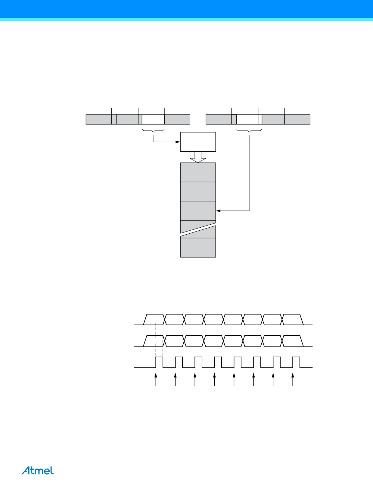
If the LSB in RDY/BSY data byte out is ‘1’, a programming operation is still pending. Wait until this bit returns ‘0’ before the
next instruction is carried out.
Within the same page, the low data byte must be loaded prior to the high data byte.
After data is loaded to the page buffer, program the EEPROM page, see Figure 27-8.
Figure 27-8. Serial Programming Instruction Example
Serial Programming Instruction
Load Program Memory Page (High/Low Byte)/
Write Program Memory Page/
Load EEPROM Memory Page (page access)
Write EEPROM Memory Page
Byte 1
Byte 2
Byte 3
Byte 4
Byte 1
Byte 2
Byte 3
Byte 4
Adr MBS
Adr LBS
Adr MBS
Adr LBS
Bit 15 B
0
Bit 15 B
0
Page Buffer
Page Offset
Page 0
Page 1
Page 2
Page Number
Page N-1
Program Memory/
EEPROM Memory
27.8.4
SPI Serial Programming Characteristics
Figure 27-9. Serial Programming Waveforms
SERIAL DATA INPUT
MSB
LSB
(MOSI)
SERIAL DATA OUTPUT
MSB
LSB
(MISO)
SERIAL CLOCK INPUT
(SCK)
SAMPLE
For characteristics of the SPI module see Section 28.7 “SPI Timing Characteristics” on page 262.
ATmega328P [DATASHEET]
257
7810D-AVR-01/15
28.
Electrical Characteristics
All DC/AC characteristics contained in this datasheet are based on characterization of Atmel® ATmega328P AVR®
microcontroller manufactured in an automotive process technology.
28.1
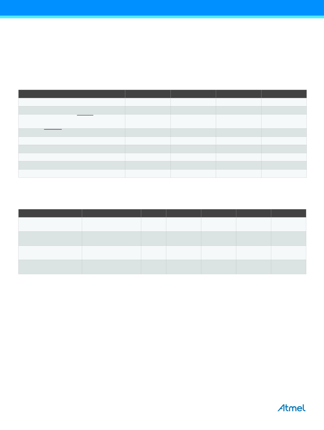
Absolute Maximum Ratings
Stresses beyond those listed under “Absolute Maximum Ratings” may cause permanent damage to the device. This is a stress rating
only and functional operation of the device at these or any other conditions beyond those indicated in the operational sections of this
specification is not implied. Exposure to absolute maximum rating conditions for extended periods may affect device reliability.
Parameters
Min.
Typ.
Max.
Unit
Operating temperature
-55
+125
°C
Storage temperature
-65
+150
°C
Voltage on any pin except RESET with respect
-0.5
VCC + 0.5
V
to ground
Voltage on RESET with respect to ground
-0.5
+13.0
V
Maximum operating voltage
6.0
V
DC current per I/O pin
40.0
mA
DC current VCC and GND pins
200.0
mA
Injection current at VCC = 0V
±5.0(1)
mA
Injection current at VCC = 5V
±1.0
mA
Note:
1.
Maximum current per port = ±30mA
28.2
DC Characteristics
TA = -40°C to +125°C, VCC = 2.7V to 5.5V (unless otherwise noted)
Parameter
Condition
Symbol
Min.
Typ.
Max.
Unit
Input low voltage, except
VCC = 2.7V to 5.5V
VIL
-0.5
0.3VCC(1)
V
XTAL1 and RESET pin
Input high voltage, except
VCC = 2.7V to 5.5V
VIH
0.6VCC(2)
VCC + 0.5
V
XTAL1 and RESET pins
Input low voltage,
VCC = 2.7V to 5.5V
VIL1
-0.5
0.1VCC(1)
V
XTAL1 pin
Input high voltage,
VCC = 2.7V to 5.5V
VIH1
0.7VCC(2)
VCC + 0.5
V
XTAL1 pin
Notes:
1.
“Max” means the highest value where the pin is guaranteed to be read as low
2.
“Min” means the lowest value where the pin is guaranteed to be read as high
3.
Although each I/O port can sink more than the test conditions (20mA at VCC = 5V, 10mA at VCC = 3V) under steady
state conditions (non-transient), the following must be observed:
ATmega328P:
1] The sum of all IOL, for ports C0 - C5, should not exceed 100mA.
2] The sum of all IOL, for ports B0 - B5, D5 - D7, XTAL1, XTAL2 should not exceed 100mA.
3] The sum of all IOL, for ports D0 - D4, should not exceed 100mA.
If IOL exceeds the test condition, VOL may exceed the related specification. Pins are not guaranteed to sink current
greater than the listed test condition.
4.
Although each I/O port can source more than the test conditions (20mA at VCC = 5V, 10mA at VCC = 3V) under steady
state conditions (non-transient), the following must be observed:
ATmega328P:
1] The sum of all IOH, for ports C0 - C5, D0- D4, should not exceed 150mA.
2] The sum of all IOH, for ports B0 - B5, D5 - D7, XTAL1, XTAL2 should not exceed 150mA.
If IIOH exceeds the test condition, VOH may exceed the related specification. Pins are not guaranteed to source current
greater than the listed test condition.
258
ATmega328P [DATASHEET]
7810D-AVR-01/15
28.2
DC Characteristics (Continued)
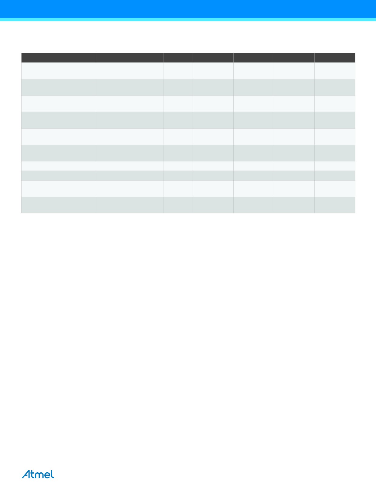
TA = -40°C to +125°C, VCC = 2.7V to 5.5V (unless otherwise noted)
Parameter
Condition
Symbol
Min.
Typ.
Max.
Unit
Input low voltage,
VCC = 2.7V to 5.5V
VIL2
-0.5
0.1VCC(1)
V
RESET pin
Input high voltage,
VCC = 2.7V to 5.5V
VIH2
0.9VCC(2)
VCC + 0.5
V
RESET pin
IOL = 20mA, VCC = 5V
0.8
Output low voltage(3)
VOL
V
IOL = 5mA, VCC
= 3V
0.5
IOH = -20mA, VCC = 5V
4.1
Output high voltage(4)
VOH
V
IOH = -10mA, VCC
= 3V
2.3
Input leakage
VCC = 5.5V, pin low
IIL
1
µA
Current I/O pin
(absolute value)
Input leakage
VCC = 5.5V, pin high
IIH
1
µA
Current I/O pin
(absolute value)
Reset pull-up resistor
RRST
30
60
k
I/O pin pull-up resistor
RPU
20
50
k
Analog comparator
0.4V < Vin < Vcc - 0.5
VACIO
10
40
mV
Input offset voltage
(absolute value)
Analog comparator
VCC = 5V
IACLK
-50
+50
nA
Input leakage current
Vin = VCC/2
Notes:
1.
“Max” means the highest value where the pin is guaranteed to be read as low
2.
“Min” means the lowest value where the pin is guaranteed to be read as high
3.
Although each I/O port can sink more than the test conditions (20mA at VCC = 5V, 10mA at VCC = 3V) under steady
state conditions (non-transient), the following must be observed:
ATmega328P:
1] The sum of all IOL, for ports C0 - C5, should not exceed 100mA.
2] The sum of all IOL, for ports B0 - B5, D5 - D7, XTAL1, XTAL2 should not exceed 100mA.
3] The sum of all IOL, for ports D0 - D4, should not exceed 100mA.
If IOL exceeds the test condition, VOL may exceed the related specification. Pins are not guaranteed to sink current
greater than the listed test condition.
4.
Although each I/O port can source more than the test conditions (20mA at VCC = 5V, 10mA at VCC = 3V) under steady
state conditions (non-transient), the following must be observed:
ATmega328P:
1] The sum of all IOH, for ports C0 - C5, D0- D4, should not exceed 150mA.
2] The sum of all IOH, for ports B0 - B5, D5 - D7, XTAL1, XTAL2 should not exceed 150mA.
If IIOH exceeds the test condition, VOH may exceed the related specification. Pins are not guaranteed to source current
greater than the listed test condition.
ATmega328P [DATASHEET]
259
7810D-AVR-01/15
28.3
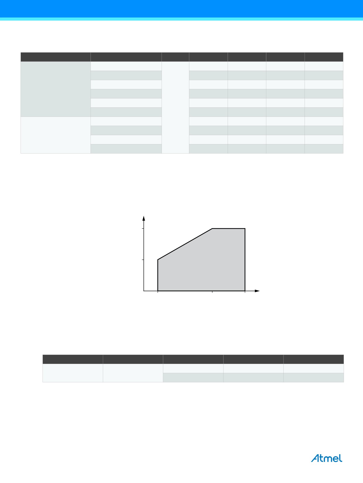
DC Characteristics
TA = -40°C to +125°C, VCC = 2.7V to 5.5V (unless otherwise noted)
Parameter
Condition
Symbol
Min.
Typ.(2)
Max.
Units
Active 4MHz, VCC = 3V
1.5
2.4
mA
Active 8MHz, VCC = 5V
5.2
10
mA
Active 16MHz, V
CC = 5V
9.2
14
mA
Power supply current(1)
Idle 4MHz, VCC = 3V
0.25
0.6
mA
Idle 8MHz, VCC = 5V
1.0
1.6
mA
I
CC
Idle 16MHz, VCC = 5V
1.9
2.8
mA
WDT enabled, VCC = 3V
44
µA
WDT enabled, VCC = 5V
66
µA
Power-down mode(3)
WDT disabled, VCC = 3V
40
µA
WDT disabled, VCC = 5V
60
µA
Notes:
1.
Values with Section 9.10 “Minimizing Power Consumption” on page 36 enabled (0xFF).
2.
Typical values at 25°C.
3.
The current consumption values include input leakage current.
28.4
Speed Grades
Figure 28-1. Maximum Frequency
16MHz
8MHz
Safe Operating Area
2.7V
4.5V
5.5V
28.5
Clock Characteristics
28.5.1
Calibrated Internal RC Oscillator Accuracy
Table 28-1. Calibration Accuracy of Internal RC Oscillator
Frequency
VCC
Temperature
Calibration Accuracy
Factory
3V
25°C
±2%
8.0MHz
Calibration
2.7V to 5.5V
-40°C to +125°C
±14%
260
ATmega328P [DATASHEET]
7810D-AVR-01/15
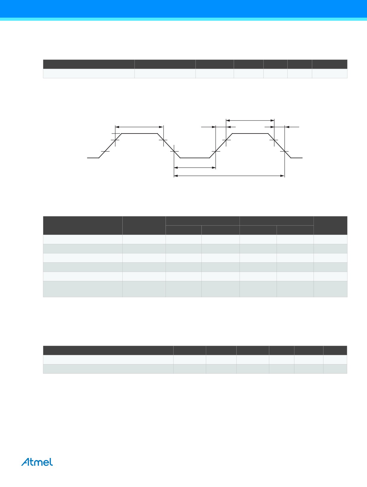
28.5.2
Watchdog Oscillator Accuracy
Table 28-2. Accuracy of Watchdog Oscillator
Parameter
Condition
Symbol
Min
Typ
Max
Unit
Watchdog oscillator frequency
Vcc = 2.7 to 5.5V
Fwdt
76
128
180
KHz
28.5.3
External Clock Drive Waveforms
Figure 28-2. External Clock Drive Waveforms
tCHCX
tCHCX
tCLCH
tCHCL
VIH1
VIL1
tCLCX
tCLCL
28.5.4
External Clock Drive
Table 28-3. External Clock Drive
VCC = 2.7 to 5.5V
VCC = 4.5 to 5.5V
Parameter
Symbol
Min.
Max.
Min.
Max.
Unit
Oscillator frequency
1/tCLCL
0
8
0
16
MHz
High time
tCHCX
50
25
ns
Low time
tCLCX
50
25
ns
Rise time
tCLCH
1.6
0.5
ns
Fall time
tCHCL
1.6
0.5
ns
Change in period from one
tCLCL
2
2
%
clock cycle to the next
Note:
All DC/AC characteristics contained in this datasheet are based on characterization of ATmega328P AVR
microcontroller manufactured in an automotive process technology.
28.6
System and Reset Characteristics
Table 28-4. Reset, Brown-out and Internal Voltage Characteristics
Parameter
Symbol
Min
Typ
Max
Unit
Brown-out detector hysteresis
VHYST
80
mV
Bandgap reference voltage
VCC = 5V
VBG
1.0
1.1
1.2
V
ATmega328P [DATASHEET]
261
7810D-AVR-01/15
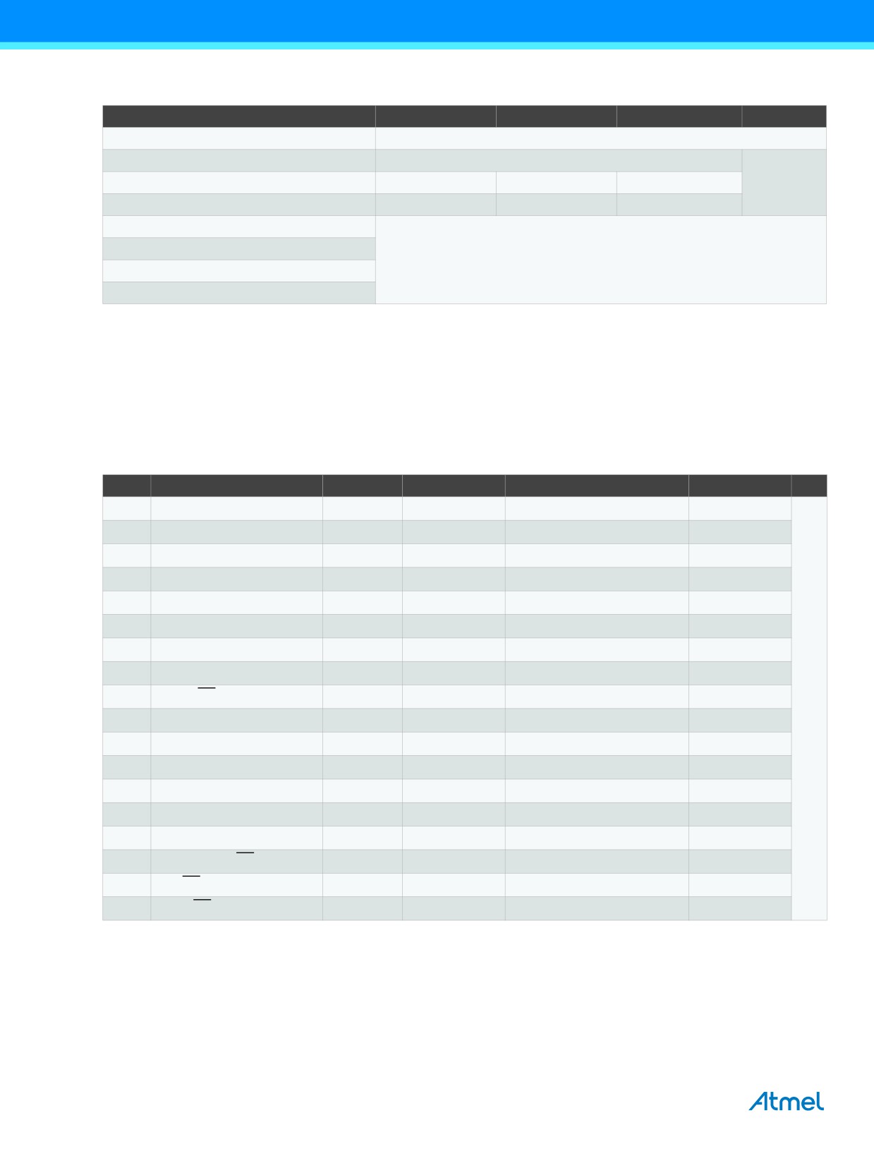
Table 28-5. BODLEVEL Fuse Coding(1)
BODLEVEL 2:0 Fuses
Min VBOT
Typ VBOT
Max VBOT
Units
111
BOD disabled
110
Reserved
101
2.5
2.7
2.9
V
100
4.0
4.3
4.6
011
010
Reserved
001
000
Note:
1.
VBOT may be below nominal minimum operating voltage for some devices. For devices where this is the case,
the device is tested down to VCC = VBOT during the production test. This guarantees that a brown-out reset will
occur before VCC drops to a voltage where correct operation of the microcontroller is no longer guaranteed.
The test is performed using BODLEVEL = 100 and BODLEVEL = 101 for ATmega328P.
28.7
SPI Timing Characteristics
See Figure 28-3 on page 263 and Figure 28-4 on page 263 for details.
Table 28-6.
SPI Timing Parameters
Description
Mode
Min
Typ
Max
1
SCK period
Master
See Table 18-5 on page 141
2
SCK high/low
Master
50% duty cycle
3
Rise/fall time
Master
3.6
4
Setup
Master
10
5
Hold
Master
10
6
Out to SCK
Master
0.5 tsck
7
SCK to out
Master
10
8
SCK to out high
Master
10
9
SS low to out
Slave
15
ns
10
SCK period
Slave
4 tck
11
SCK high/low(1)
Slave
2 tck
12
Rise/fall time
Slave
1600
13
Setup
Slave
10
14
Hold
Slave
tck
15
SCK to out
Slave
15
16
SCK to SS high
Slave
20
17
SS high to tri-state
Slave
10
18
SS low to SCK
Slave
20
Notes:
1.
In SPI programming mode the minimum SCK high/low period is:
- 2 tCLCL for fCK < 12MHz
- 3 tCLCL for fCK > 12MHz
2.
All AC/AC characteristics contained in this datasheet are based on characterization of ATmega328P AVR
®
microcontroller manufactured in an automotive process technology.
262
ATmega328P [DATASHEET]
7810D-AVR-01/15
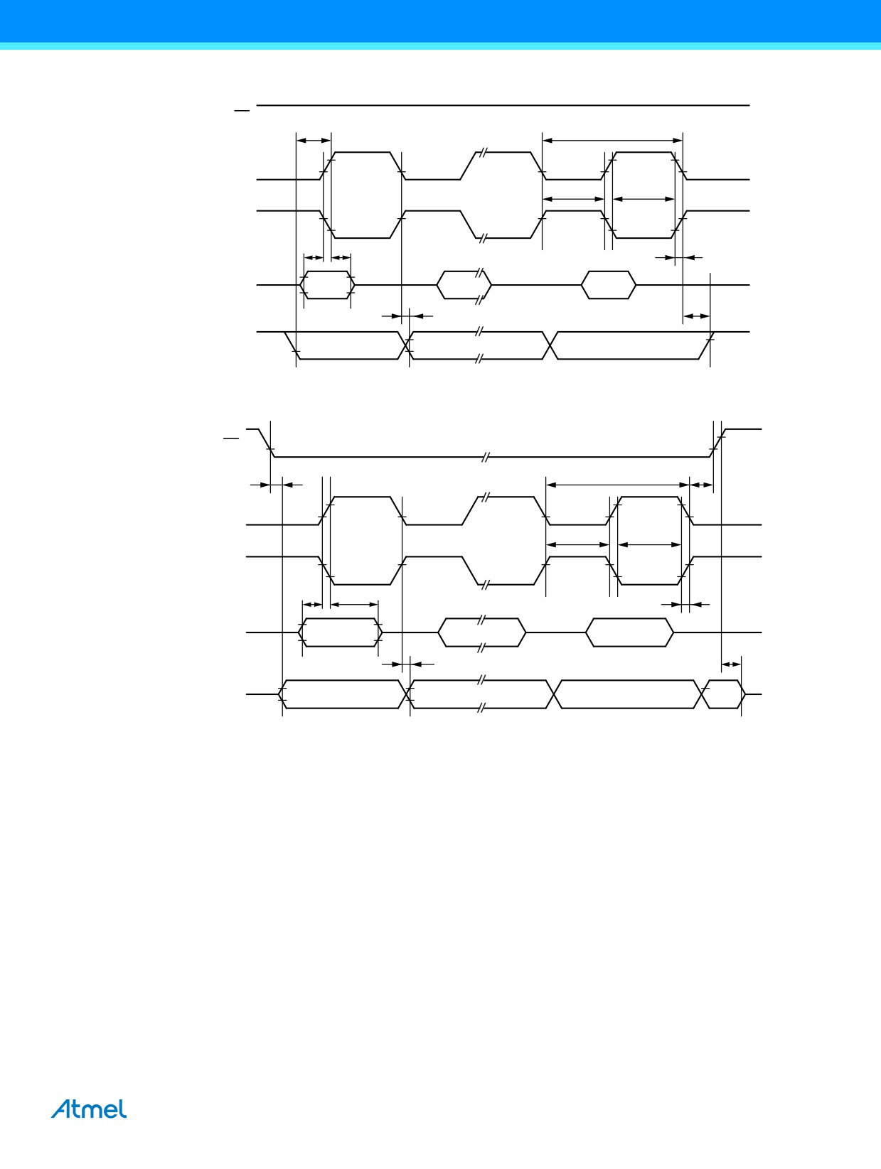
Figure 28-3. SPI Interface Timing Requirements (Master Mode)
SS
6
1
SCK
(CPOL = 0)
2
2
SCK
(CPOL = 1)
4
5
3
MISO
MSB
LSB
(Data Input)
7
8
MOSI
MSB
LSB
(Data Output)
Figure 28-4. SPI Interface Timing Requirements (Slave Mode)
SS
9
10
16
SCK
(CPOL = 0)
11
11
SCK
(CPOL = 1)
13
14
12
MOSI
MSB
LSB
(Data Input)
15
17
MISO
MSB
LSB
X
(Data Output)
ATmega328P [DATASHEET]
263
7810D-AVR-01/15

28.8
2-wire Serial Interface Characteristics
Table 28-7 describes the requirements for devices connected to the 2-wire serial bus. The Atmel® ATmega328P 2-wire serial
interface meets or exceeds these requirements under the noted conditions.
Timing symbols refer to Figure 28-5 on page 265.
Table 28-7.
2-wire Serial Bus Requirements
Parameter
Condition
Symbol
Min
Max
Units
Input low-voltage
VIL
-0.5
0.3 VCC
V
Input high-voltage
VIH
0.7 VCC
V
V
CC + 0.5
Hysteresis of schmitt trigger inputs
Vhys(1)
0.05 VCC(2)
-
V
Output low-voltage
3mA sink current
VOL(1)
0
0.4
V
Rise time for both SDA and SCL
tr(1)
20 + 0.1Cb(3)(2)
300
ns
Output fall time from VIHmin to VILmax
10pF < Cb < 400pF(3)
tof(1)
20 + 0.1Cb(3)(2)
250
ns
Spikes suppressed by input filter
tSP(1)
0
50(2)
ns
Input current each I/O pin
0.1VCC < Vi < 0.9VCC
Ii
-10
10
µA
Capacitance for each I/O pin
Ci(1)
-
10
pF
SCL clock frequency
f
(4) >max(16fSCL, 250kHz)(5)
fSCL
0
400
kHz
CK
VCC
– 0.4V
f
----------------------------
---------------
SCL ≤ 100kHz
3mA
C
b
Value of pull-up resistor
Rp
VCC
- 0.4V
f
----------------------------
-------------
SCL > 100kHz
3mA
C
b
f
4.0
-
µs
SCL ≤ 100kHz
Hold time (repeated) START condition
tHD;STA
f
0.6
-
µs
SCL > 100kHz
f
4.7
-
µs
SCL ≤ 100kHz
Low period of the SCL clock
tLOW
f
1.3
-
µs
SCL > 100kHz
f
4.0
-
µs
SCL ≤ 100kHz
High period of the SCL clock
tHIGH
f
0.6
-
µs
SCL > 100kHz
f
4.7
-
µs
Set-up time for a repeated START
SCL ≤ 100kHz
tSU;STA
condition
f
0.6
-
µs
SCL > 100kHz
f
0
3.45
µs
SCL ≤ 100kHz
Data hold time
tHD;DAT
f
0
0.9
µs
SCL > 100kHz
f
250
-
ns
SCL ≤ 100kHz
Data setup time
tSU;DAT
f
100
-
ns
SCL > 100kHz
f
4.0
-
µs
SCL ≤ 100kHz
Setup time for STOP condition
tSU;STO
f
0.6
-
µs
SCL > 100kHz
f
4.7
-
µs
Bus free time between a STOP and
SCL ≤ 100kHz
tBUF
START condition
f
1.3
-
µs
SCL > 100kHz
Notes:
1.
In Atmel ATmega328P, this parameter is characterized and not 100% tested.
2.
Required only for fSCL > 100kHz.
3.
Cb = capacitance of one bus line in pF.
4.
fCK = CPU clock frequency
5.
This requirement applies to all Atmel ATmega328P 2-wire serial interface operation. Other devices connected
to the 2-wire serial bus need only obey the general fSCL requirement.
264
ATmega328P [DATASHEET]
7810D-AVR-01/15
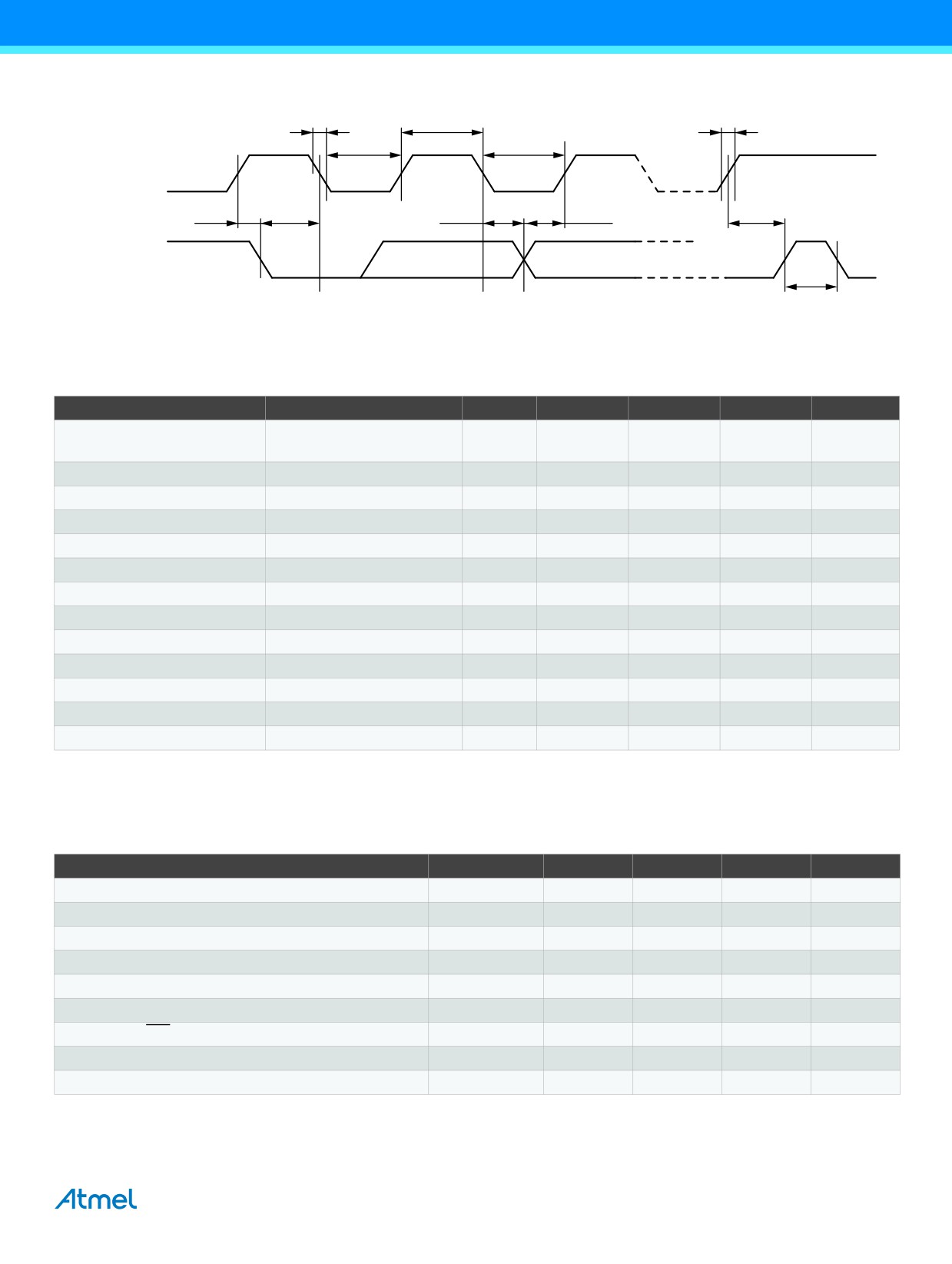
Figure 28-5. 2-wire Serial Bus Timing
tof
tHIGH
t
r
tLOW
tLOW
SCL
tSU,STA
tHD,STA
tHD,DAT
t
t
SU,DAT
SU,STO
SDA
t
BUF
28.9
ADC Characteristics
Table 28-8. ADC Characteristics
Parameter
Condition
Symbol
Min
Typ
Max
Unit
-40°C +125°C / 2.70 to 5.50V
Resolution
10
bits
ADC clock = 200kHz
Absolute accuracy
Vcc = 4.0V,VREF = 4.0V
TUE
2.2
3.5
LSB
Integral non linearity
Vcc = 4.0V, VREF = 4.0V
INL
0.6
1.5
LSB
Differential non linearity
Vcc = 4.0V, VREF = 4.0V
DNL
0.3
0.7
LSB
Gain error
Vcc = 4.0V, VREF = 4.0V
-3.5
+3.5
LSB
Offset error
Vcc = 4.0V, VREF = 4.0V
-3.5
+3.5
LSB
Clock frequency
50
200
kHz
Analog supply voltage
AVCC
Vcc - 0.3
Vcc + 0.3
V
Reference voltage
VREF
1.0
AVCC
V
Input voltage
Vin
GND
VREF
V
Internal voltage reference
Vcc = 5v
Vint
1.0
1.1
1.2
V
Reference input resistance
Rref
22.4
32
41.6
k
Analog input resistance
Rain
100
M
28.10
Parallel Programming Characteristics
Table 28-9. Parallel Programming Characteristics, VCC = 5V ±10%
Parameter
Symbol
Min
Typ
Max
Units
Programming enable voltage
VPP
11.5
12.5
V
Programming enable current
IPP
250
µA
Data and control valid before XTAL1 high
tDVXH
67
ns
XTAL1 low to XTAL1 high
tXLXH
200
ns
XTAL1 pulse width high
tXHXL
150
ns
Data and control hold after XTAL1 low
tXLDX
67
ns
XTAL1 low to WR low
tXLWL
0
ns
XTAL1 low to PAGEL high
tXLPH
0
ns
PAGEL low to XTAL1 high
tPLXH
150
ns
Notes:
1.
tWLRH is valid for the write flash, write EEPROM, write fuse bits and write lock bits commands.
2.
tWLRH_CE is valid for the chip erase command.
ATmega328P [DATASHEET]
265
7810D-AVR-01/15
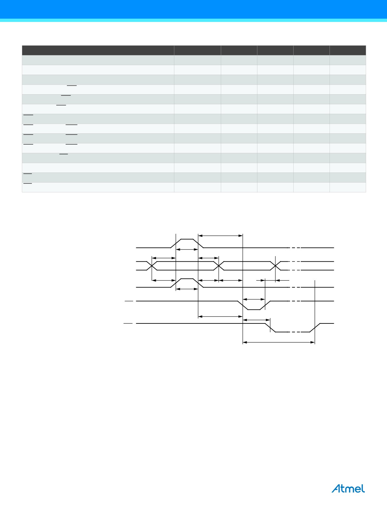
Table 28-9. Parallel Programming Characteristics, VCC = 5V ±10% (Continued)
Parameter
Symbol
Min
Typ
Max
Units
BS1 valid before PAGEL high
tBVPH
67
ns
PAGEL pulse width high
tPHPL
150
ns
BS1 hold after PAGEL low
tPLBX
67
ns
BS2/1 hold after WR low
tWLBX
67
ns
PAGEL low to WR low
tPLWL
67
ns
BS1 valid to WR low
tBVWL
67
ns
WR pulse Width low
tWLWH
150
ns
WR low to RDY/BSY low
tWLRL
0
1
µs
WR low to RDY/BSY high(1)
tWLRH
3.7
4.5
ms
WR low to RDY/BSY high for chip erase(2)
tWLRH_CE
7.5
9
ms
XTAL1 low to OE low
tXLOL
0
ns
BS1 valid to DATA valid
tBVDV
0
250
ns
OE low to DATA valid
tOLDV
250
ns
OE high to DATA tri-stated
tOHDZ
250
ns
Notes:
1.
tWLRH is valid for the write flash, write EEPROM, write fuse bits and write lock bits commands.
2.
tWLRH_CE is valid for the chip erase command.
Figure 28-6. Parallel Programming Timing, Including some General Timing Requirements
tXLWL
XTAL1
tXHXL
tDVXH
tXLDX
Data and Control
(DATA, XA0/1, BS1, BS2)
tBVPH
tPLBX
tBVWL
tWLBX
PAGEL
tPHPL
tWLWH
WR
tPLWL
tWLRL
RDY/BSY
tWLRH
266
ATmega328P [DATASHEET]
7810D-AVR-01/15
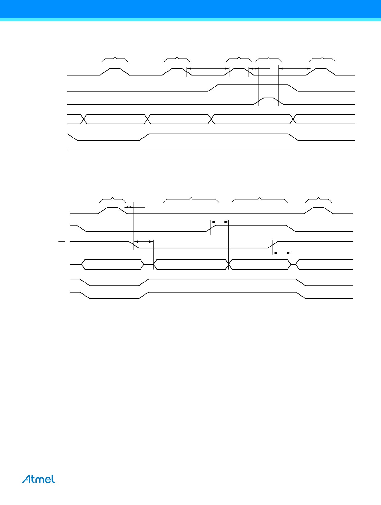
Figure 28-7. Parallel Programming Timing, Loading Sequence with Timing Requirements(1)
Load Address
Load Data
Load Data
Load Address
(Low Byte)
(Low Byte)
(High Byte)
Load Data
(Low Byte)
tXLXH
tXLPH
tPLXH
XTAL1
BS1
PAGEL
DATA
ADDR0 (Low Byte)
DATA (Low Byte)
DATA (High Byte)
ADDR1 (Low Byte)
XA0
XA1
Note:
1.
The timing requirements shown in Figure 28-6 (i.e., tDVXH, tXHXL, and tXLDX) also apply to loading operation.
Figure 28-8. Parallel Programming Timing, Reading Sequence (within the Same Page) with Timing Requirements(1)
Load Address
Read Data
Read Data
Load Address
(Low Byte)
(Low Byte)
(High Byte)
(Low Byte)
tXLOL
XTAL1
tBVDV
BS1
tOLDV
OE
t
OHDZ
DATA
ADDR0 (Low Byte)
DATA (Low Byte)
DATA (High Byte)
ADDR1 (Low Byte)
XA0
XA1
Note:
1.
The timing requirements shown in Figure 28-6 on page 266 (i.e., tDVXH, tXHXL, and tXLDX) also apply to reading
operation.
ATmega328P [DATASHEET]
267
7810D-AVR-01/15
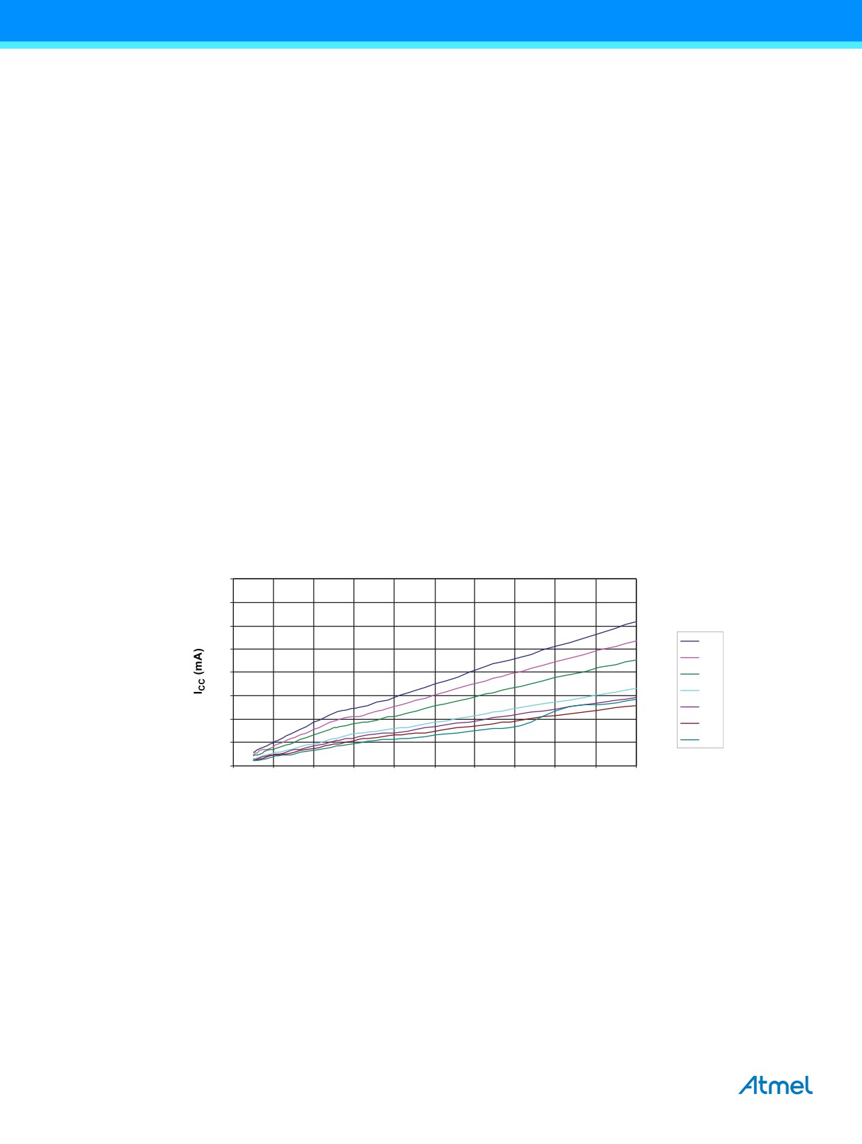
29.
Typical Characteristics
The data contained in this section are characterized values of actual automotive silicon. Unless otherwise specified, the data
contained in this chapter are for -40° to 125°C.
The following charts show typical behavior. These figures are not tested during manufacturing. All current consumption
measurements are performed with all I/O pins configured as inputs and with internal pull-ups enabled. A square wave
generator with rail-to-rail output is used as clock source.
All Active- and idle current consumption measurements are done with all bits in the PRR register set and thus, the
corresponding I/O modules are turned off. Also the analog comparator is disabled during these measurements. The “supply
current of IO modules” shows the additional current consumption compared to ICC active and ICC idle for every I/O module
controlled by the power reduction register. See Section 9.9 “Power Reduction Register” on page 36 for details.
The power consumption in power-down mode is independent of clock selection.
The current consumption is a function of several factors such as: operating voltage, operating frequency, loading of I/O pins,
switching rate of I/O pins, code executed and ambient temperature. The dominating factors are operating voltage and
frequency.
The current drawn from capacitive loaded pins may be estimated (for one pin) as CL VCC f where CL = load capacitance,
VCC = operating voltage and f = average switching frequency of I/O pin.
The parts are characterized at frequencies higher than test limits. Parts are not guaranteed to function properly at
frequencies higher than the ordering code indicates.
The difference between current consumption in power-down mode with watchdog timer enabled and power-down mode with
watchdog timer disabled represents the differential current drawn by the watchdog timer.
29.1
ATmega328P Typical Characteristics
29.1.1
Active Supply Current
Figure 29-1. Active Supply Current versus Frequency
16
14
12
5.5
10
5.0
8
4.5
3.6
6
3.3
4
3.0
2.7
2
0
0
2
4
6
8
10
12
14
16
18
20
Frequency (MHz)
268
ATmega328P [DATASHEET]
7810D-AVR-01/15
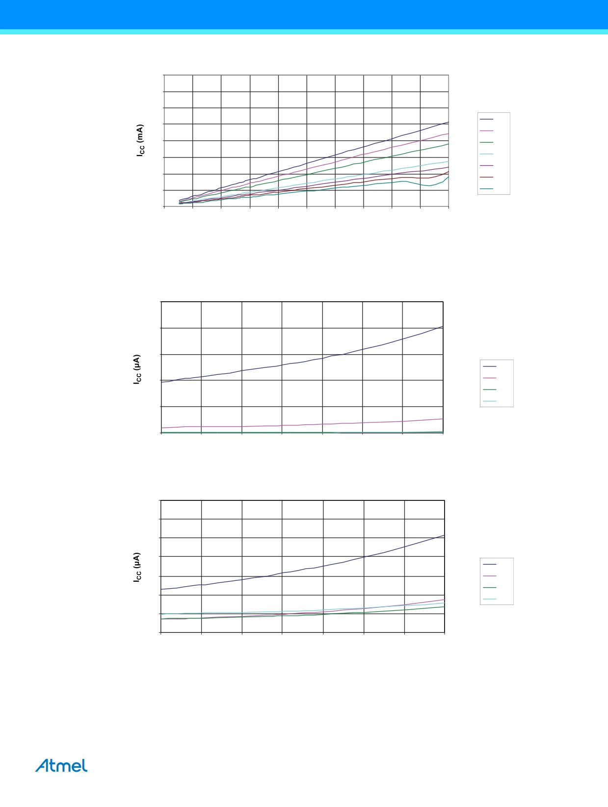
Figure 29-2. Idle Supply Current versus Frequency
4
3.5
3
5.5
2.5
5.0
2
4.5
3.6
1.5
3.3
1
3.0
2.7
0.5
0
0
2
4
6
8
10
12
14
16
18
20
Frequency (MHz)
29.1.2
Power-down Supply Current
Figure 29-3. Power-Down Supply Current versus VCC (Watchdog Timer Disabled)
25
20
15
125
85
10
25
-45
5
0
2
2.5
3
3.5
4
4.5
5
5.5
VCC (V)
Figure 29-4. Power-Down Supply Current versus VCC (Watchdog Timer Enabled)
35
30
25
20
125
15
85
25
10
-45
5
0
2
2.5
3
3.5
4
4.5
5
5.5
VCC (V)
ATmega328P [DATASHEET]
269
7810D-AVR-01/15
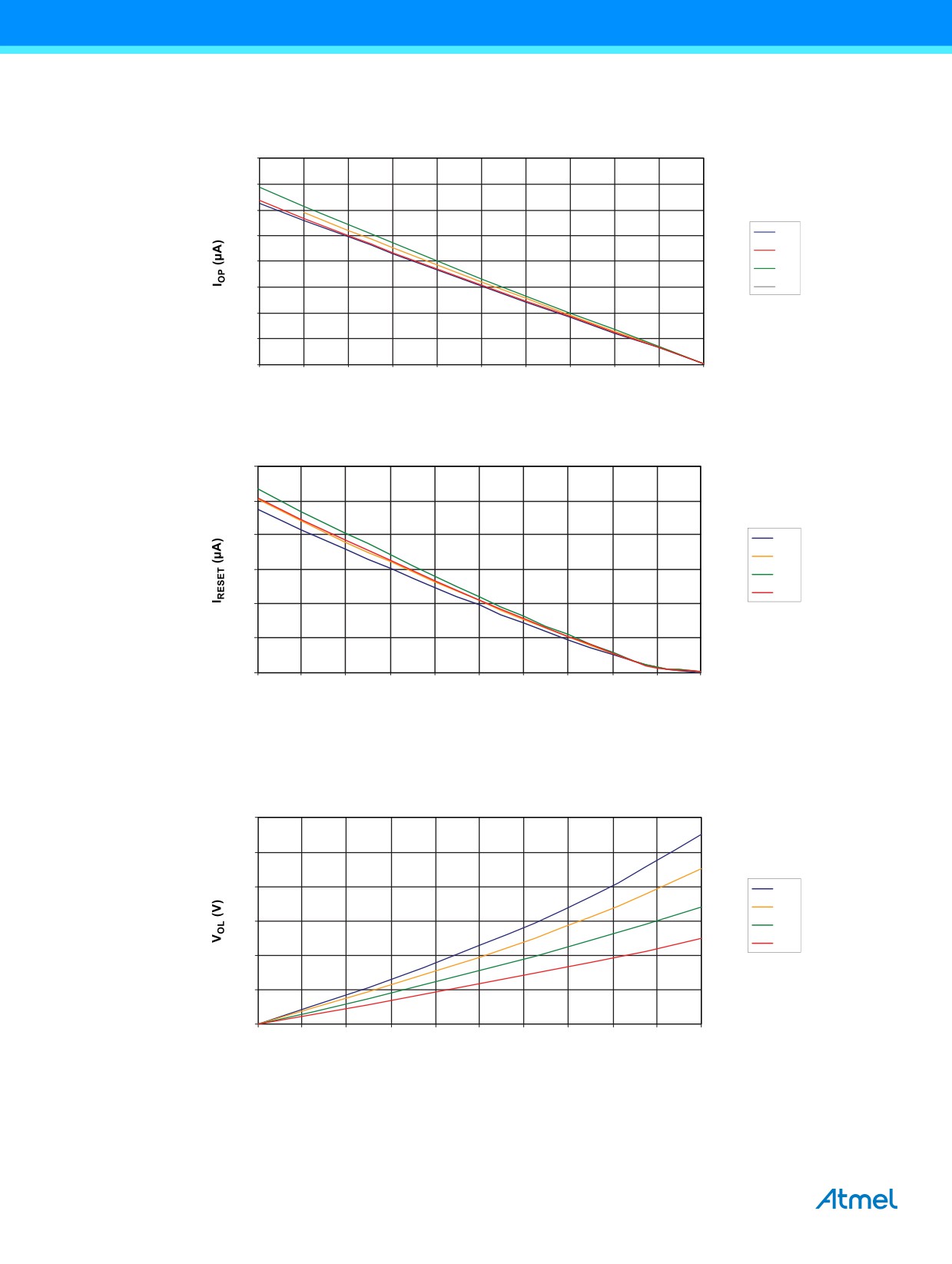
29.1.3
Pin Pull-Up
Figure 29-5. I/O Pin Pull-up Resistor Current versus Input Voltage (VCC = 5V)
160
140
120
125
100
85
80
25
60
-45
40
20
0
0
0.5
1
1.5
2
2.5
3
3.5
4
4.5
5
VOP (V)
Figure 29-6. Reset Pull-up Resistor Current versus Reset Pin Voltage (VCC = 5 V)
120
100
80
125
85
60
25
-45
40
20
0
0
0.5
1
1.5
2
2.5
3
3.5
4
4.5
5
VRESET (V)
29.1.4
Pin Driver Strength
Figure 29-7. I/O Pin Output Voltage versus Sink Current (VCC = 3 V)
1.2
1
0.8
125
85
0.6
25
-45
0.4
0.2
0
0
2
4
6
8
10
12
14
16
18
20
IOL (mA)
270
ATmega328P [DATASHEET]
7810D-AVR-01/15
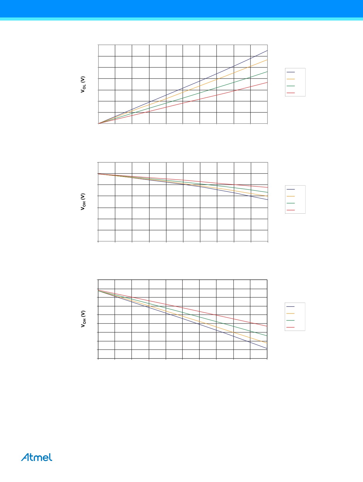
Figure 29-8. I/O Pin Output Voltage versus Sink Current (VCC = 5 V)
0.7
0.6
0.5
125
0.4
85
25
0.3
-45
0.2
0.1
0
0
2
4
6
8
10
12
14
16
18
20
IOL (mA)
Figure 29-9. I/O Pin Output Voltage versus Source Current (VCC = 3 V)
3.5
3
2.5
125
2
85
25
1.5
-45
1
0.5
0
0
2
4
6
8
10
12
14
16
18
20
IOH (mA)
Figure 29-10.
I/O Pin Output Voltage versus Source Current (VCC = 5 V)
5.1
5
4.9
4.8
125
85
4.7
25
4.6
-45
4.5
4.4
4.3
4.2
0
2
4
6
8
10
12
14
16
18
20
IOH (mA)
ATmega328P [DATASHEET]
271
7810D-AVR-01/15
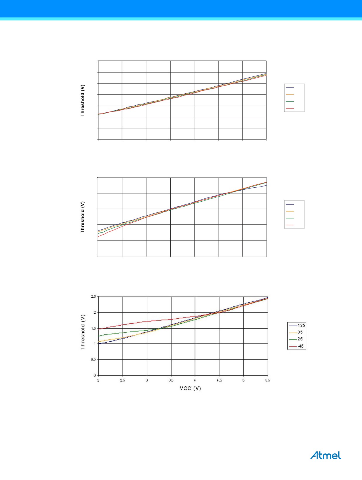
29.1.5
Pin Threshold and Hysteresis
Figure 29-11.
I/O Pin Input Threshold Voltage versus VCC (VIH, I/O Pin read as ‘1’)
3.5
3
2.5
125
2
85
25
1.5
-45
1
0.5
0
2
2.5
3
3.5
4
4.5
5
5.5
VCC (V)
Figure 29-12.
I/O Pin Input Threshold Voltage versus VCC (VIL, I/O Pin read as ‘0’)
2.5
2
125
1.5
85
25
1
-45
0.5
0
2
2.5
3
3.5
4
4.5
5
5.5
VCC (V)
Figure 29-13.
Reset Input Threshold Voltage versus VCC (VIH, I/O Pin read as ‘1’)
272
ATmega328P [DATASHEET]
7810D-AVR-01/15
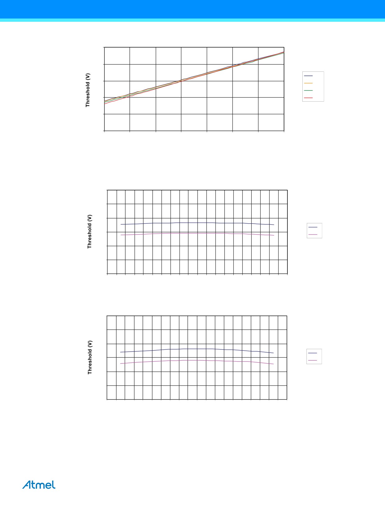
Figure 29-14. Reset Input Threshold Voltage versus VCC (VIL, I/O Pin read as ‘0’)
2.5
2
125
1.5
85
25
1
-45
0.5
0
2
2.5
3
3.5
4
4.5
5
5.5
VCC (V)
29.1.6
BOD Threshold
Figure 29-15.
BOD Thresholds versus Temperature (BODLEVEL is 2.7V)
3
2.9
2.8
1
2.7
0
2.6
2.5
2.4
-60 -50
-40
-30 -20
-10
0
10
20
30
40
50
60
70
80
90
100
110
120
130
140
Temperature (°C)
Figure 29-16.
BOD Thresholds versus Temperature (BODLEVEL is 4.3V)
4.6
4.5
4.4
1
4.3
0
4.2
4.1
4
-60 -50
-40
-30 -20
-10
0
10
20
30
40
50
60
70
80
90
100 110 120 130 140
Temperature (°C)
ATmega328P [DATASHEET]
273
7810D-AVR-01/15
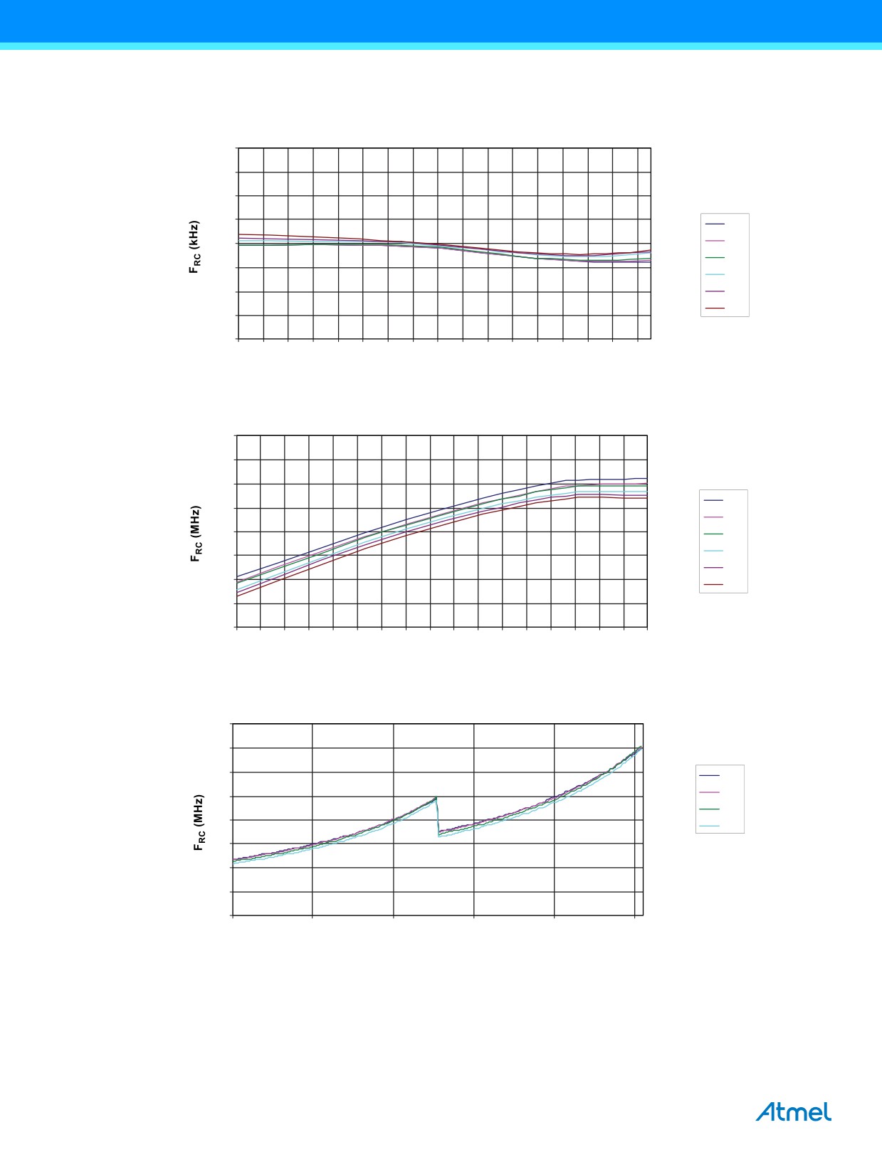
29.1.7
Internal Oscillator Speed
Figure 29-17.
Watchdog Oscillator Frequency versus Temperature
160
150
140
130
5.5
5.0
120
4.5
110
3.3
100
3.0
2.7
90
80
-40
-30
-20
-10
0
10
20
30
40
50
60
70
80
90
100
110
120
Temperature (°C)
Figure 29-18.
Calibrated 8MHz RC Oscillator Frequency versus Temperature
8.4
8.3
8.2
5.5
8.1
5.0
8
4.5
3.3
7.9
3.0
7.8
2.7
7.7
7.6
-45
-35
-25
-15
-5
5
15
25
35
45
55
65
75
85
95
105
115
125
Temperature (°C)
Figure 29-19.
Calibrated 8MHz RC Oscillator Frequency versus OSCCAL Value
16
14
12
125
85
10
25
8
-45
6
4
2
0
0
50
100
150
200
250
OSCCAL (X1)
274
ATmega328P [DATASHEET]
7810D-AVR-01/15
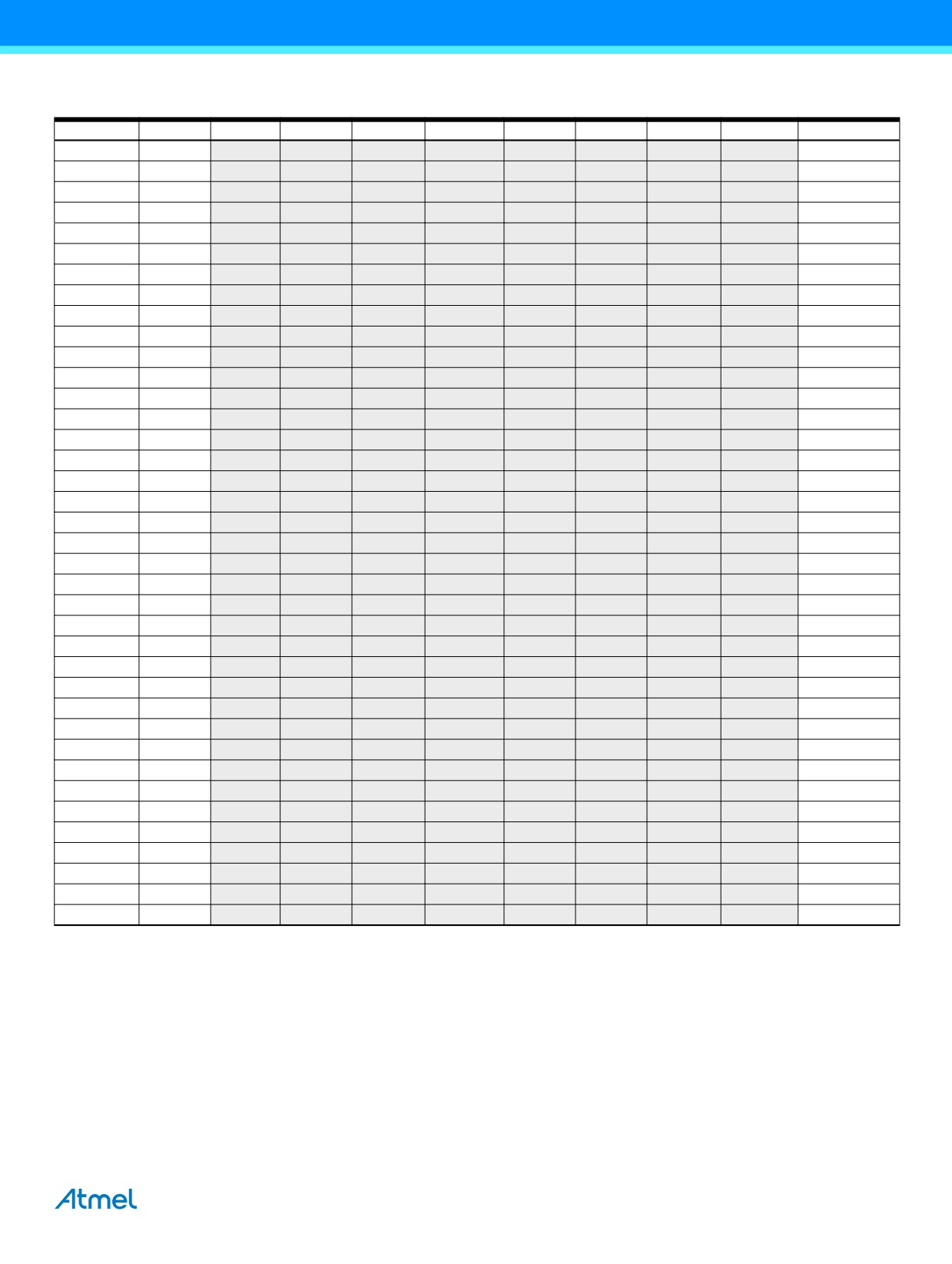
30.
Register Summary
Address
Name
Bit 7
Bit 6
Bit 5
Bit 4
Bit 3
Bit 2
Bit 1
Bit 0
Page
(0xFF)
Reserved
-
-
-
-
-
-
-
-
(0xFE)
Reserved
-
-
-
-
-
-
-
-
(0xFD)
Reserved
-
-
-
-
-
-
-
-
(0xFC)
Reserved
-
-
-
-
-
-
-
-
(0xFB)
Reserved
-
-
-
-
-
-
-
-
(0xFA)
Reserved
-
-
-
-
-
-
-
-
(0xF9)
Reserved
-
-
-
-
-
-
-
-
(0xF8)
Reserved
-
-
-
-
-
-
-
-
(0xF7)
Reserved
-
-
-
-
-
-
-
-
(0xF6)
Reserved
-
-
-
-
-
-
-
-
(0xF5)
Reserved
-
-
-
-
-
-
-
-
(0xF4)
Reserved
-
-
-
-
-
-
-
-
(0xF3)
Reserved
-
-
-
-
-
-
-
-
(0xF2)
Reserved
-
-
-
-
-
-
-
-
(0xF1)
Reserved
-
-
-
-
-
-
-
-
(0xF0)
Reserved
-
-
-
-
-
-
-
-
(0xEF)
Reserved
-
-
-
-
-
-
-
-
(0xEE)
Reserved
-
-
-
-
-
-
-
-
(0xED)
Reserved
-
-
-
-
-
-
-
-
(0xEC)
Reserved
-
-
-
-
-
-
-
-
(0xEB)
Reserved
-
-
-
-
-
-
-
-
(0xEA)
Reserved
-
-
-
-
-
-
-
-
(0xE9)
Reserved
-
-
-
-
-
-
-
-
(0xE8)
Reserved
-
-
-
-
-
-
-
-
(0xE7)
Reserved
-
-
-
-
-
-
-
-
(0xE6)
Reserved
-
-
-
-
-
-
-
-
(0xE5)
Reserved
-
-
-
-
-
-
-
-
(0xE4)
Reserved
-
-
-
-
-
-
-
-
(0xE3)
Reserved
-
-
-
-
-
-
-
-
(0xE2)
Reserved
-
-
-
-
-
-
-
-
(0xE1)
Reserved
-
-
-
-
-
-
-
-
(0xE0)
Reserved
-
-
-
-
-
-
-
-
(0xDF)
Reserved
-
-
-
-
-
-
-
-
(0xDE)
Reserved
-
-
-
-
-
-
-
-
(0xDD)
Reserved
-
-
-
-
-
-
-
-
(0xDC)
Reserved
-
-
-
-
-
-
-
-
(0xDB)
Reserved
-
-
-
-
-
-
-
-
(0xDA)
Reserved
-
-
-
-
-
-
-
-
Notes:
1.
For compatibility with future devices, reserved bits should be written to zero if accessed. Reserved I/O memory
addresses should never be written.
2.
I/O registers within the address range 0x00 - 0x1F are directly bit-accessible using the SBI and CBI instructions. In
these registers, the value of single bits can be checked by using the SBIS and SBIC instructions.
3.
Some of the status flags are cleared by writing a logical one to them. Note that, unlike most other AVR®, the CBI and
SBI instructions will only operate on the specified bit, and can therefore be used on registers containing such status
flags. The CBI and SBI instructions work with registers 0x00 to 0x1F only.
4.
When using the I/O specific commands IN and OUT, the I/O addresses 0x00 - 0x3F must be used. When addressing
I/O registers as data space using LD and ST instructions, 0x20 must be added to these addresses. The ATmega328P
is a complex microcontroller with more peripheral units than can be supported within the 64 location reserved in opcode
for the IN and OUT instructions. For the extended I/O space from 0x60 - 0xFF in SRAM, only the ST/STS/STD and
LD/LDS/LDD instructions can be used.
ATmega328P [DATASHEET]
275
7810D-AVR-01/15
30.
Register Summary (Continued)
Address
Name
Bit 7
Bit 6
Bit 5
Bit 4
Bit 3
Bit 2
Bit 1
Bit 0
Page
(0xD9)
Reserved
-
-
-
-
-
-
-
-
(0xD8)
Reserved
-
-
-
-
-
-
-
-
(0xD7)
Reserved
-
-
-
-
-
-
-
-
(0xD6)
Reserved
-
-
-
-
-
-
-
-
(0xD5)
Reserved
-
-
-
-
-
-
-
-
(0xD4)
Reserved
-
-
-
-
-
-
-
-
(0xD3)
Reserved
-
-
-
-
-
-
-
-
(0xD2)
Reserved
-
-
-
-
-
-
-
-
(0xD1)
Reserved
-
-
-
-
-
-
-
-
(0xD0)
Reserved
-
-
-
-
-
-
-
-
(0xCF)
Reserved
-
-
-
-
-
-
-
-
(0xCE)
Reserved
-
-
-
-
-
-
-
-
(0xCD)
Reserved
-
-
-
-
-
-
-
-
(0xCC)
Reserved
-
-
-
-
-
-
-
-
(0xCB)
Reserved
-
-
-
-
-
-
-
-
(0xCA)
Reserved
-
-
-
-
-
-
-
-
(0xC9)
Reserved
-
-
-
-
-
-
-
-
(0xC8)
Reserved
-
-
-
-
-
-
-
-
(0xC7)
Reserved
-
-
-
-
-
-
-
-
(0xC6)
UDR0
USART I/O data register
159
(0xC5)
UBRR0H
USART baud rate register high
162
(0xC4)
UBRR0L
USART baud rate register low
162
(0xC3)
Reserved
-
-
-
-
-
-
-
-
UCSZ01
UCSZ00 /
(0xC2)
UCSR0C
UMSEL01
UMSEL00
UPM01
UPM00
USBS0
UCPOL0
161/172
/UDORD0
UCPHA0
(0xC1)
UCSR0B
RXCIE0
TXCIE0
UDRIE0
RXEN0
TXEN0
UCSZ02
RXB80
TXB80
160
(0xC0)
UCSR0A
RXC0
TXC0
UDRE0
FE0
DOR0
UPE0
U2X0
MPCM0
159
(0xBF)
Reserved
-
-
-
-
-
-
-
-
(0xBE)
Reserved
-
-
-
-
-
-
-
-
(0xBD)
TWAMR
TWAM6
TWAM5
TWAM4
TWAM3
TWAM2
TWAM1
TWAM0
-
201
(0xBC)
TWCR
TWINT
TWEA
TWSTA
TWSTO
TWWC
TWEN
-
TWIE
199
(0xBB)
TWDR
2-wire serial interface data register
200
(0xBA)
TWAR
TWA6
TWA5
TWA4
TWA3
TWA2
TWA1
TWA0
TWGCE
201
(0xB9)
TWSR
TWS7
TWS6
TWS5
TWS4
TWS3
-
TWPS1
TWPS0
200
(0xB8)
TWBR
2-wire serial interface bit rate register
198
(0xB7)
Reserved
-
-
-
-
-
-
-
(0xB6)
ASSR
-
EXCLK
AS2
TCN2UB
OCR2AUB
OCR2BUB
TCR2AUB
TCR2BUB
133
(0xB5)
Reserved
-
-
-
-
-
-
-
-
Notes:
1.
For compatibility with future devices, reserved bits should be written to zero if accessed. Reserved I/O memory
addresses should never be written.
2.
I/O registers within the address range 0x00 - 0x1F are directly bit-accessible using the SBI and CBI instructions. In
these registers, the value of single bits can be checked by using the SBIS and SBIC instructions.
3.
Some of the status flags are cleared by writing a logical one to them. Note that, unlike most other AVR®, the CBI and
SBI instructions will only operate on the specified bit, and can therefore be used on registers containing such status
flags. The CBI and SBI instructions work with registers 0x00 to 0x1F only.
4.
When using the I/O specific commands IN and OUT, the I/O addresses 0x00 - 0x3F must be used. When addressing
I/O registers as data space using LD and ST instructions, 0x20 must be added to these addresses. The ATmega328P
is a complex microcontroller with more peripheral units than can be supported within the 64 location reserved in opcode
for the IN and OUT instructions. For the extended I/O space from 0x60 - 0xFF in SRAM, only the ST/STS/STD and
LD/LDS/LDD instructions can be used.
276
ATmega328P [DATASHEET]
7810D-AVR-01/15
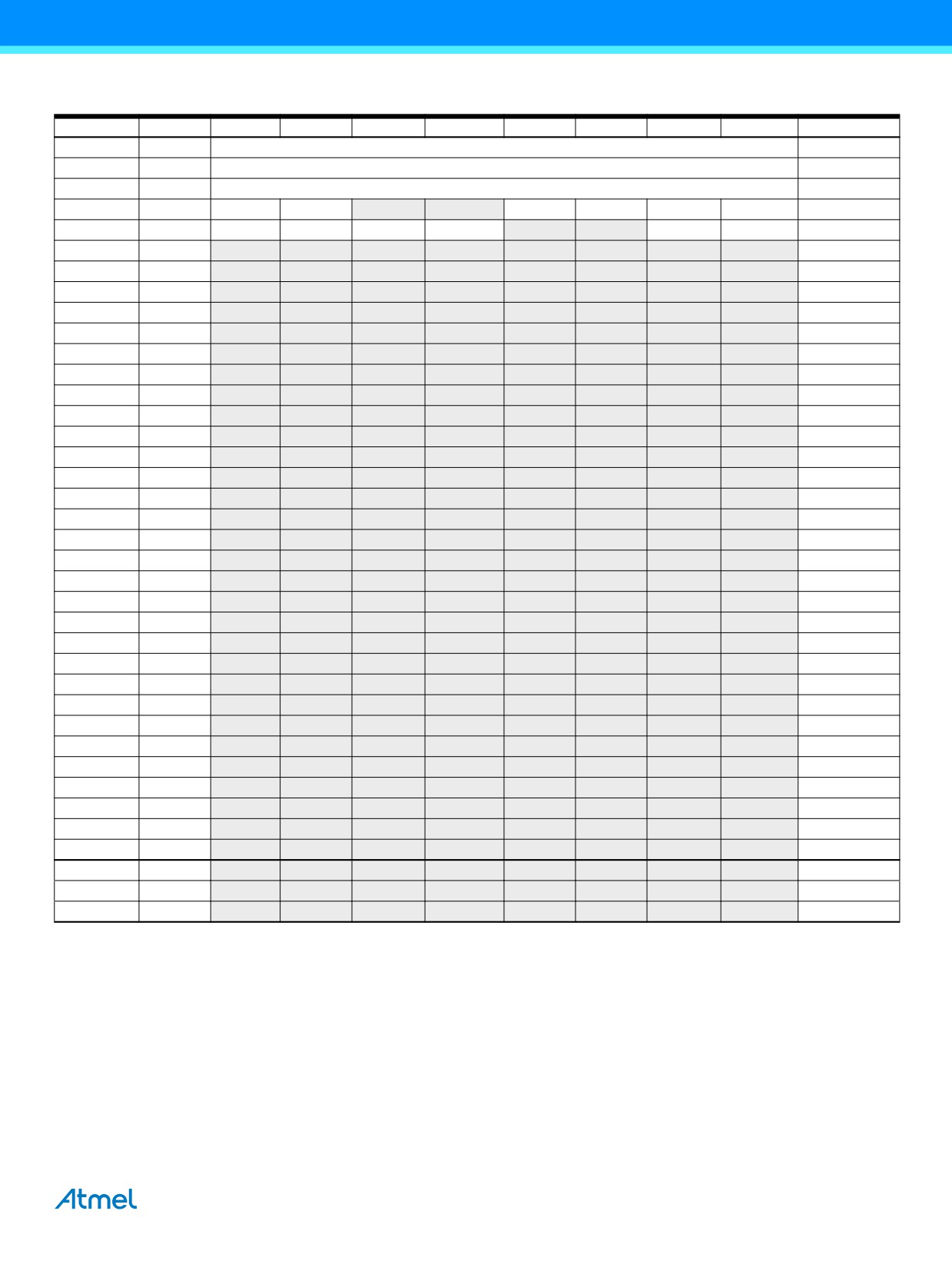
30.
Register Summary (Continued)
Address
Name
Bit 7
Bit 6
Bit 5
Bit 4
Bit 3
Bit 2
Bit 1
Bit 0
Page
(0xB4)
OCR2B
Timer/Counter2 output compare register B
131
(0xB3)
OCR2A
Timer/Counter2 output compare register A
131
(0xB2)
TCNT2
Timer/Counter2 (8-bit)
131
(0xB1)
TCCR2B
FOC2A
FOC2B
-
-
WGM22
CS22
CS21
CS20
130
(0xB0)
TCCR2A
COM2A1
COM2A0
COM2B1
COM2B0
-
-
WGM21
WGM20
127
(0xAF)
Reserved
-
-
-
-
-
-
-
-
(0xAE)
Reserved
-
-
-
-
-
-
-
-
(0xAD)
Reserved
-
-
-
-
-
-
-
-
(0xAC)
Reserved
-
-
-
-
-
-
-
-
(0xAB)
Reserved
-
-
-
-
-
-
-
-
(0xAA)
Reserved
-
-
-
-
-
-
-
-
(0xA9)
Reserved
-
-
-
-
-
-
-
-
(0xA8)
Reserved
-
-
-
-
-
-
-
-
(0xA7)
Reserved
-
-
-
-
-
-
-
-
(0xA6)
Reserved
-
-
-
-
-
-
-
-
(0xA5)
Reserved
-
-
-
-
-
-
-
-
(0xA4)
Reserved
-
-
-
-
-
-
-
-
(0xA3)
Reserved
-
-
-
-
-
-
-
-
(0xA2)
Reserved
-
-
-
-
-
-
-
-
(0xA1)
Reserved
-
-
-
-
-
-
-
-
(0xA0)
Reserved
-
-
-
-
-
-
-
-
(0x9F)
Reserved
-
-
-
-
-
-
-
-
(0x9E)
Reserved
-
-
-
-
-
-
-
-
(0x9D)
Reserved
-
-
-
-
-
-
-
-
(0x9C)
Reserved
-
-
-
-
-
-
-
-
(0x9B)
Reserved
-
-
-
-
-
-
-
-
(0x9A)
Reserved
-
-
-
-
-
-
-
-
(0x99)
Reserved
-
-
-
-
-
-
-
-
(0x98)
Reserved
-
-
-
-
-
-
-
-
(0x97)
Reserved
-
-
-
-
-
-
-
-
(0x96)
Reserved
-
-
-
-
-
-
-
-
(0x95)
Reserved
-
-
-
-
-
-
-
-
(0x94)
Reserved
-
-
-
-
-
-
-
-
(0x93)
Reserved
-
-
-
-
-
-
-
-
(0x92)
Reserved
-
-
-
-
-
-
-
-
(0x91)
Reserved
-
-
-
-
-
-
-
-
(0x90)
Reserved
-
-
-
-
-
-
-
-
(0x8F)
Reserved
-
-
-
-
-
-
-
-
Notes:
1.
For compatibility with future devices, reserved bits should be written to zero if accessed. Reserved I/O memory
addresses should never be written.
2.
I/O registers within the address range 0x00 - 0x1F are directly bit-accessible using the SBI and CBI instructions. In
these registers, the value of single bits can be checked by using the SBIS and SBIC instructions.
3.
Some of the status flags are cleared by writing a logical one to them. Note that, unlike most other AVR®, the CBI and
SBI instructions will only operate on the specified bit, and can therefore be used on registers containing such status
flags. The CBI and SBI instructions work with registers 0x00 to 0x1F only.
4.
When using the I/O specific commands IN and OUT, the I/O addresses 0x00 - 0x3F must be used. When addressing
I/O registers as data space using LD and ST instructions, 0x20 must be added to these addresses. The ATmega328P
is a complex microcontroller with more peripheral units than can be supported within the 64 location reserved in opcode
for the IN and OUT instructions. For the extended I/O space from 0x60 - 0xFF in SRAM, only the ST/STS/STD and
LD/LDS/LDD instructions can be used.
ATmega328P [DATASHEET]
277
7810D-AVR-01/15
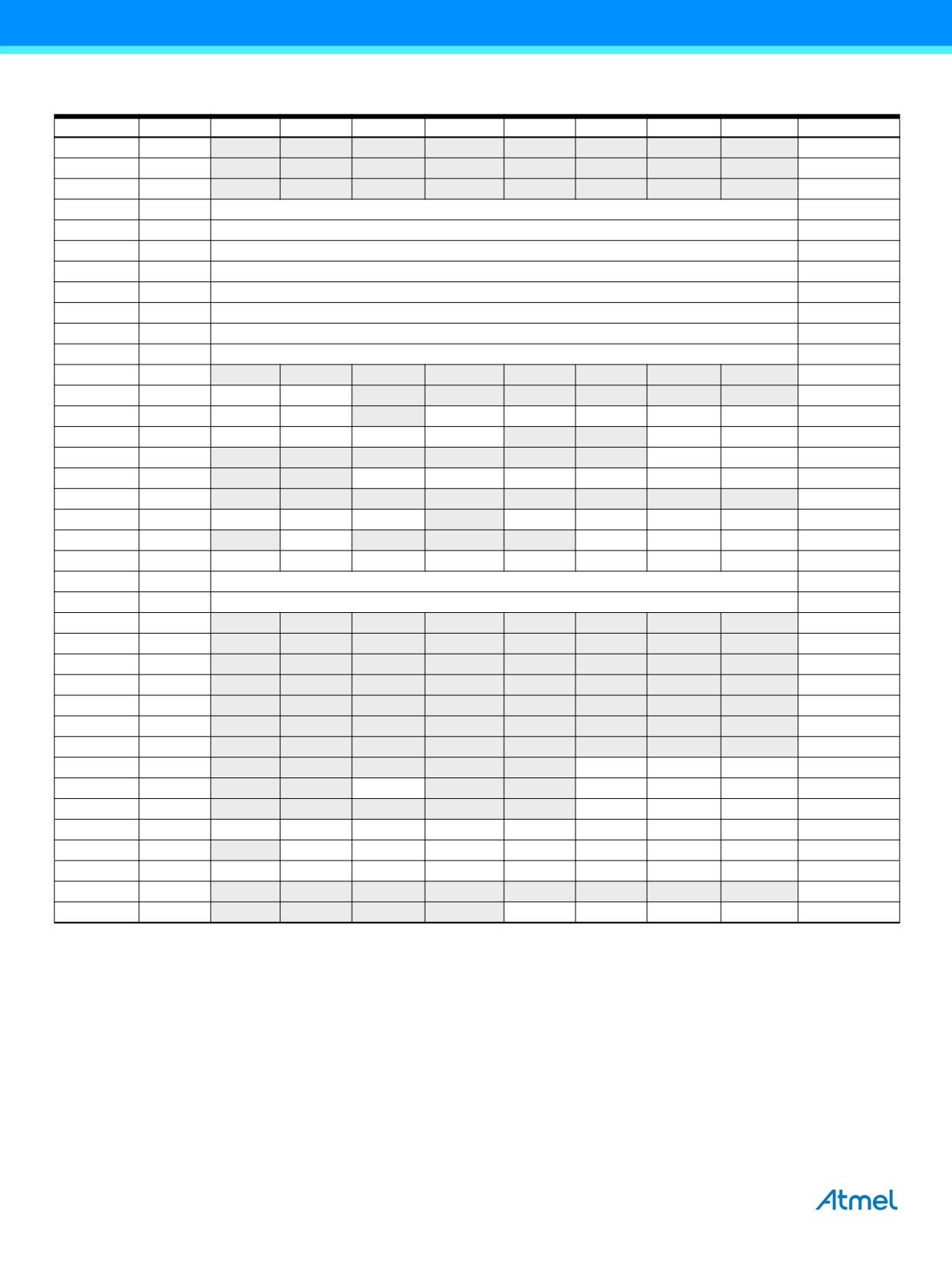
30.
Register Summary (Continued)
Address
Name
Bit 7
Bit 6
Bit 5
Bit 4
Bit 3
Bit 2
Bit 1
Bit 0
Page
(0x8E)
Reserved
-
-
-
-
-
-
-
-
(0x8D)
Reserved
-
-
-
-
-
-
-
-
(0x8C)
Reserved
-
-
-
-
-
-
-
-
(0x8B)
OCR1BH
Timer/Counter1 - Output compare register B high byte
111
(0x8A)
OCR1BL
Timer/Counter1 - Output compare register B low byte
111
(0x89)
OCR1AH
Timer/Counter1 - Output compare register A high byte
111
(0x88)
OCR1AL
Timer/Counter1 - Output compare register A low byte
111
(0x87)
ICR1H
Timer/Counter1 - Input capture register high byte
112
(0x86)
ICR1L
Timer/Counter1 - Input capture register low byte
112
(0x85)
TCNT1H
Timer/Counter1 - Counter register high byte
111
(0x84)
TCNT1L
Timer/Counter1 - Counter register low byte
111
(0x83)
Reserved
-
-
-
-
-
-
-
-
(0x82)
TCCR1C
FOC1A
FOC1B
-
-
-
-
-
-
111
(0x81)
TCCR1B
ICNC1
ICES1
-
WGM13
WGM12
CS12
CS11
CS10
110
(0x80)
TCCR1A
COM1A1
COM1A0
COM1B1
COM1B0
-
-
WGM11
WGM10
108
(0x7F)
DIDR1
-
-
-
-
-
-
AIN1D
AIN0D
204
(0x7E)
DIDR0
-
-
ADC5D
ADC4D
ADC3D
ADC2D
ADC1D
ADC0D
220
(0x7D)
Reserved
-
-
-
-
-
-
-
-
(0x7C)
ADMUX
REFS1
REFS0
ADLAR
-
MUX3
MUX2
MUX1
MUX0
217
(0x7B)
ADCSRB
-
ACME
-
-
-
ADTS2
ADTS1
ADTS0
220
(0x7A)
ADCSRA
ADEN
ADSC
ADATE
ADIF
ADIE
ADPS2
ADPS1
ADPS0
218
(0x79)
ADCH
ADC data register high byte
219
(0x78)
ADCL
ADC data register low byte
219
(0x77)
Reserved
-
-
-
-
-
-
-
-
(0x76)
Reserved
-
-
-
-
-
-
-
-
(0x75)
Reserved
-
-
-
-
-
-
-
-
(0x74)
Reserved
-
-
-
-
-
-
-
-
(0x73)
Reserved
-
-
-
-
-
-
-
-
(0x72)
Reserved
-
-
-
-
-
-
-
-
(0x71)
Reserved
-
-
-
-
-
-
-
-
(0x70)
TIMSK2
-
-
-
-
-
OCIE2B
OCIE2A
TOIE2
132
(0x6F)
TIMSK1
-
-
ICIE1
-
-
OCIE1B
OCIE1A
TOIE1
112
(0x6E)
TIMSK0
-
-
-
-
-
OCIE0B
OCIE0A
TOIE0
88
(0x6D)
PCMSK2
PCINT23
PCINT22
PCINT21
PCINT20
PCINT19
PCINT18
PCINT17
PCINT16
57
(0x6C)
PCMSK1
-
PCINT14
PCINT13
PCINT12
PCINT11
PCINT10
PCINT9
PCINT8
57
(0x6B)
PCMSK0
PCINT7
PCINT6
PCINT5
PCINT4
PCINT3
PCINT2
PCINT1
PCINT0
57
(0x6A)
Reserved
-
-
-
-
-
-
-
-
(0x69)
EICRA
-
-
-
-
ISC11
ISC10
ISC01
ISC00
54
Notes:
1.
For compatibility with future devices, reserved bits should be written to zero if accessed. Reserved I/O memory
addresses should never be written.
2.
I/O registers within the address range 0x00 - 0x1F are directly bit-accessible using the SBI and CBI instructions. In
these registers, the value of single bits can be checked by using the SBIS and SBIC instructions.
3.
Some of the status flags are cleared by writing a logical one to them. Note that, unlike most other AVR®, the CBI and
SBI instructions will only operate on the specified bit, and can therefore be used on registers containing such status
flags. The CBI and SBI instructions work with registers 0x00 to 0x1F only.
4.
When using the I/O specific commands IN and OUT, the I/O addresses 0x00 - 0x3F must be used. When addressing
I/O registers as data space using LD and ST instructions, 0x20 must be added to these addresses. The ATmega328P
is a complex microcontroller with more peripheral units than can be supported within the 64 location reserved in opcode
for the IN and OUT instructions. For the extended I/O space from 0x60 - 0xFF in SRAM, only the ST/STS/STD and
LD/LDS/LDD instructions can be used.
278
ATmega328P [DATASHEET]
7810D-AVR-01/15
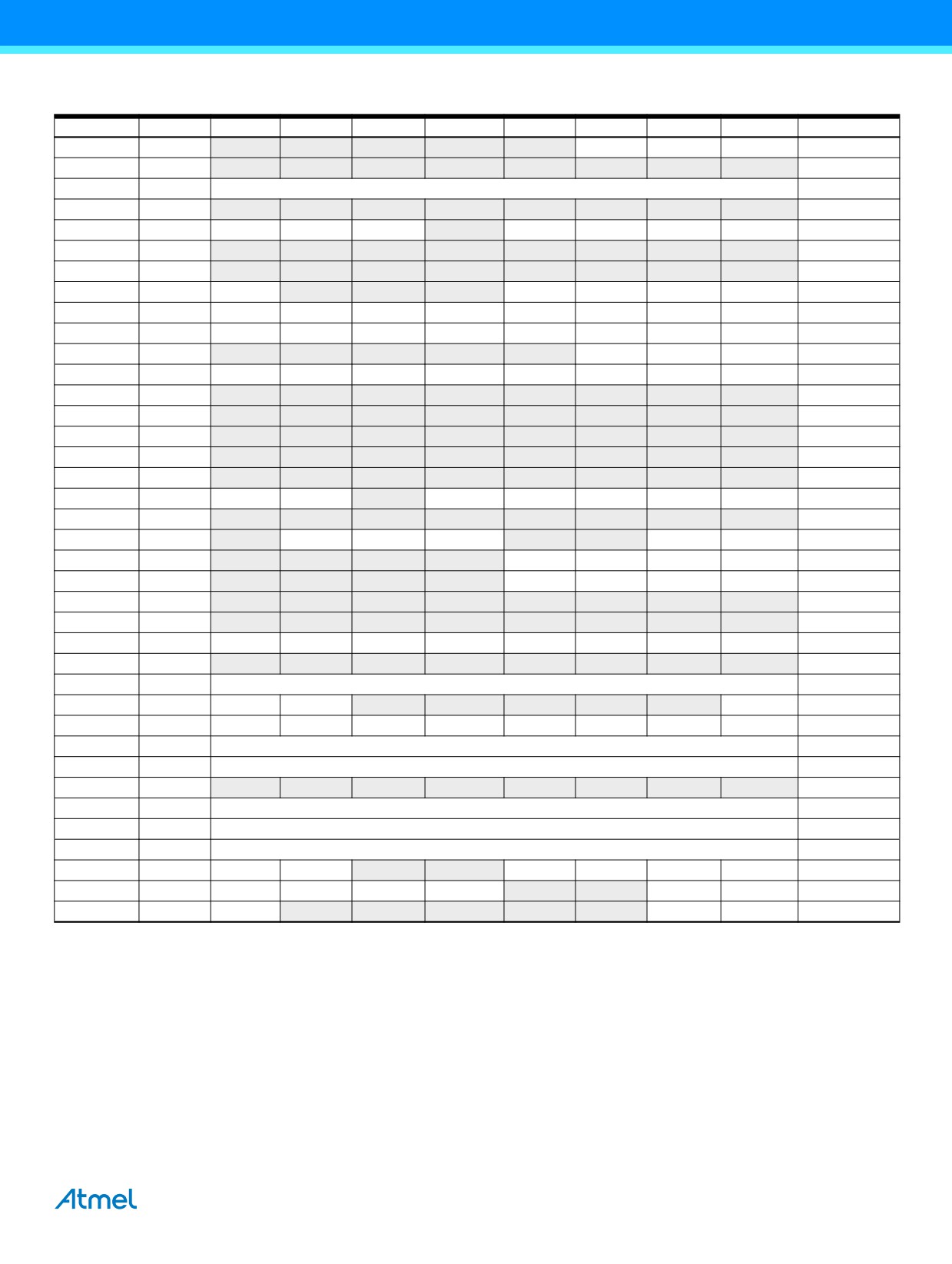
30.
Register Summary (Continued)
Address
Name
Bit 7
Bit 6
Bit 5
Bit 4
Bit 3
Bit 2
Bit 1
Bit 0
Page
(0x68)
PCICR
-
-
-
-
-
PCIE2
PCIE1
PCIE0
(0x67)
Reserved
-
-
-
-
-
-
-
-
(0x66)
OSCCAL
Oscillator calibration register
32
(0x65)
Reserved
-
-
-
-
-
-
-
-
(0x64)
PRR
PRTWI
PRTIM2
PRTIM0
-
PRTIM1
PRSPI
PRUSAR0
PRADC
36
(0x63)
Reserved
-
-
-
-
-
-
-
-
(0x62)
Reserved
-
-
-
-
-
-
-
-
(0x61)
CLKPR
CLKPCE
-
-
-
CLKPS3
CLKPS2
CLKPS1
CLKPS0
33
(0x60)
WDTCSR
WDIF
WDIE
WDP3
WDCE
WDE
WDP2
WDP1
WDP0
47
0x3F (0x5F)
SREG
I
T
H
S
V
N
Z
C
10
0x3E (0x5E)
SPH
-
-
-
-
-
(SP10)
SP9
SP8
13
0x3D (0x5D)
SPL
SP7
SP6
SP5
SP4
SP3
SP2
SP1
SP0
13
0x3C (0x5C)
Reserved
-
-
-
-
-
-
-
-
0x3B (0x5B)
Reserved
-
-
-
-
-
-
-
-
0x3A (0x5A)
Reserved
-
-
-
-
-
-
-
-
0x39 (0x59)
Reserved
-
-
-
-
-
-
-
-
0x38 (0x58)
Reserved
-
-
-
-
-
-
-
-
0x37 (0x57)
SPMCSR
SPMIE
(RWWSB)
-
(RWWSRE)
BLBSET
PGWRT
PGERS
SELFPRGN
239
0x36 (0x56)
Reserved
-
-
-
-
-
-
-
-
0x35 (0x55)
MCUCR
-
BODS
BODSE
PUD
-
-
IVSEL
IVCE
38/52/72
0x34 (0x54)
MCUSR
-
-
-
-
WDRF
BORF
EXTRF
PORF
46
0x33 (0x53)
SMCR
-
-
-
-
SM2
SM1
SM0
SE
35
0x32 (0x52)
Reserved
-
-
-
-
-
-
-
-
0x31 (0x51)
Reserved
-
-
-
-
-
-
-
-
0x30 (0x50)
ACSR
ACD
ACBG
ACO
ACI
ACIE
ACIC
ACIS1
ACIS0
203
0x2F (0x4F)
Reserved
-
-
-
-
-
-
-
-
0x2E (0x4E)
SPDR
SPI data register
142
0x2D (0x4D)
SPSR
SPIF
WCOL
-
-
-
-
-
SPI2X
141
0x2C (0x4C)
SPCR
SPIE
SPE
DORD
MSTR
CPOL
CPHA
SPR1
SPR0
140
0x2B (0x4B)
GPIOR2
General purpose I/O register 2
23
0x2A (0x4A)
GPIOR1
General purpose I/O register 1
23
0x29 (0x49)
Reserved
-
-
-
-
-
-
-
-
0x28 (0x48)
OCR0B
Timer/Counter0 output compare register B
0x27 (0x47)
OCR0A
Timer/Counter0 output compare register A
0x26 (0x46)
TCNT0
Timer/Counter0 (8-bit)
0x25 (0x45)
TCCR0B
FOC0A
FOC0B
-
-
WGM02
CS02
CS01
CS00
0x24 (0x44)
TCCR0A
COM0A1
COM0A0
COM0B1
COM0B0
-
-
WGM01
WGM00
0x23 (0x43)
GTCCR
TSM
-
-
-
-
-
PSRASY
PSRSYNC
115/134
Notes:
1.
For compatibility with future devices, reserved bits should be written to zero if accessed. Reserved I/O memory
addresses should never be written.
2.
I/O registers within the address range 0x00 - 0x1F are directly bit-accessible using the SBI and CBI instructions. In
these registers, the value of single bits can be checked by using the SBIS and SBIC instructions.
3.
Some of the status flags are cleared by writing a logical one to them. Note that, unlike most other AVR®, the CBI and
SBI instructions will only operate on the specified bit, and can therefore be used on registers containing such status
flags. The CBI and SBI instructions work with registers 0x00 to 0x1F only.
4.
When using the I/O specific commands IN and OUT, the I/O addresses 0x00 - 0x3F must be used. When addressing
I/O registers as data space using LD and ST instructions, 0x20 must be added to these addresses. The ATmega328P
is a complex microcontroller with more peripheral units than can be supported within the 64 location reserved in opcode
for the IN and OUT instructions. For the extended I/O space from 0x60 - 0xFF in SRAM, only the ST/STS/STD and
LD/LDS/LDD instructions can be used.
ATmega328P [DATASHEET]
279
7810D-AVR-01/15