Atmel ATmega328P 8-bit AVR Microcontroller. DATASHEET (2015) - page 8
30.
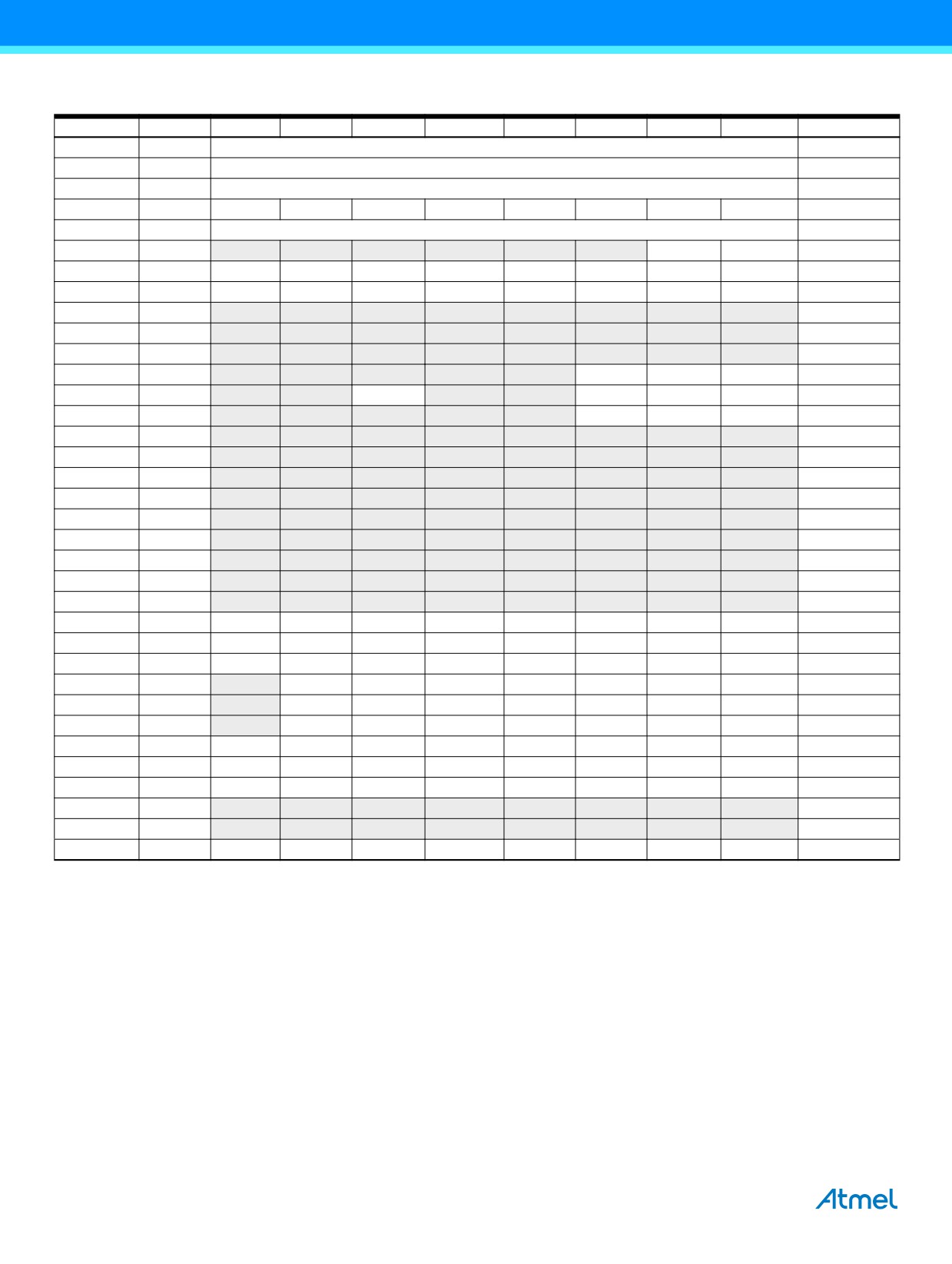
Register Summary (Continued)
Address
Name
Bit 7
Bit 6
Bit 5
Bit 4
Bit 3
Bit 2
Bit 1
Bit 0
Page
0x22 (0x42)
EEARH
(EEPROM address register high byte)
20
0x21 (0x41)
EEARL
EEPROM address register low byte
20
0x20 (0x40)
EEDR
EEPROM data register
20
0x1F (0x3F)
EECR
-
-
EEPM1
EEPM0
EERIE
EEMPE
EEPE
EERE
20
0x1E (0x3E)
GPIOR0
General purpose I/O register 0
23
0x1D (0x3D)
EIMSK
-
-
-
-
-
-
INT1
INT0
55
0x1C (0x3C)
EIFR
-
-
-
-
-
-
INTF1
INTF0
55
0x1B (0x3B)
PCIFR
-
-
-
-
-
PCIF2
PCIF1
PCIF0
0x1A (0x3A)
Reserved
-
-
-
-
-
-
-
-
0x19 (0x39)
Reserved
-
-
-
-
-
-
-
-
0x18 (0x38)
Reserved
-
-
-
-
-
-
-
-
0x17 (0x37)
TIFR2
-
-
-
-
-
OCF2B
OCF2A
TOV2
132
0x16 (0x36)
TIFR1
-
-
ICF1
-
-
OCF1B
OCF1A
TOV1
113
0x15 (0x35)
TIFR0
-
-
-
-
-
OCF0B
OCF0A
TOV0
0x14 (0x34)
Reserved
-
-
-
-
-
-
-
-
0x13 (0x33)
Reserved
-
-
-
-
-
-
-
-
0x12 (0x32)
Reserved
-
-
-
-
-
-
-
-
0x11 (0x31)
Reserved
-
-
-
-
-
-
-
-
0x10 (0x30)
Reserved
-
-
-
-
-
-
-
-
0x0F (0x2F)
Reserved
-
-
-
-
-
-
-
-
0x0E (0x2E)
Reserved
-
-
-
-
-
-
-
-
0x0D (0x2D)
Reserved
-
-
-
-
-
-
-
-
0x0C (0x2C)
Reserved
-
-
-
-
-
-
-
-
0x0B (0x2B)
PORTD
PORTD7
PORTD6
PORTD5
PORTD4
PORTD3
PORTD2
PORTD1
PORTD0
73
0x0A (0x2A)
DDRD
DDD7
DDD6
DDD5
DDD4
DDD3
DDD2
DDD1
DDD0
73
0x09 (0x29)
PIND
PIND7
PIND6
PIND5
PIND4
PIND3
PIND2
PIND1
PIND0
73
0x08 (0x28)
PORTC
-
PORTC6
PORTC5
PORTC4
PORTC3
PORTC2
PORTC1
PORTC0
73
0x07 (0x27)
DDRC
-
DDC6
DDC5
DDC4
DDC3
DDC2
DDC1
DDC0
73
0x06 (0x26)
PINC
-
PINC6
PINC5
PINC4
PINC3
PINC2
PINC1
PINC0
73
0x05 (0x25)
PORTB
PORTB7
PORTB6
PORTB5
PORTB4
PORTB3
PORTB2
PORTB1
PORTB0
72
0x04 (0x24)
DDRB
DDB7
DDB6
DDB5
DDB4
DDB3
DDB2
DDB1
DDB0
72
0x03 (0x23)
PINB
PINB7
PINB6
PINB5
PINB4
PINB3
PINB2
PINB1
PINB0
72
0x02 (0x22)
Reserved
-
-
-
-
-
-
-
-
0x01 (0x21)
Reserved
-
-
-
-
-
-
-
-
0x0 (0x20)
Reserved
-
-
-
-
-
-
-
-
Notes:
1.
For compatibility with future devices, reserved bits should be written to zero if accessed. Reserved I/O memory
addresses should never be written.
2.
I/O registers within the address range 0x00 - 0x1F are directly bit-accessible using the SBI and CBI instructions. In
these registers, the value of single bits can be checked by using the SBIS and SBIC instructions.
3.
Some of the status flags are cleared by writing a logical one to them. Note that, unlike most other AVR®, the CBI and
SBI instructions will only operate on the specified bit, and can therefore be used on registers containing such status
flags. The CBI and SBI instructions work with registers 0x00 to 0x1F only.
4.
When using the I/O specific commands IN and OUT, the I/O addresses 0x00 - 0x3F must be used. When addressing
I/O registers as data space using LD and ST instructions, 0x20 must be added to these addresses. The ATmega328P
is a complex microcontroller with more peripheral units than can be supported within the 64 location reserved in opcode
for the IN and OUT instructions. For the extended I/O space from 0x60 - 0xFF in SRAM, only the ST/STS/STD and
LD/LDS/LDD instructions can be used.
280
ATmega328P [DATASHEET]
7810D-AVR-01/15
31.
Instruction Set Summary
Mnemonics
Operands
Description
Operation
Flags
#Clocks
Arithmetic and Logic Instructions
ADD
Rd, Rr
Add two registers
Rd Rd + Rr
Z,C,N,VH
1
ADC
Rd, Rr
Add with carry two registers
Rd Rd + Rr + C
Z,C,N,V,H
1
ADIW
Rdl, K
Add immediate to word
Rdh: Rdl Rdh: Rdl + K
Z,C,N,V,S
2
SUB
Rd, Rr
Subtract two registers
Rd Rd - Rr
Z,C,N,V,H
1
SUBI
Rd, K
Subtract constant from register
Rd Rd - K
Z,C,N,V,H
1
SBC
Rd, Rr
Subtract with carry two registers
Rd Rd - Rr - C
Z,C,N,V,H
1
Subtract with carry constant from
SBCI
Rd, K
Rd Rd - K - C
Z,C,N,V,H
1
reg.
SBIW
Rdl, K
Subtract immediate from word
Rdh: Rdl Rdh: Rdl - K
Z,C,N,V,S
2
AND
Rd, Rr
Logical AND registers
Rd Rd Rr
Z,N,V
1
ANDI
Rd, K
Logical AND register and constant
Rd Rd K
Z,N,V
1
OR
Rd, Rr
Logical OR registers
Rd Rd v Rr
Z,N,V
1
ORI
Rd, K
Logical OR register and constant
Rd Rd v K
Z,N,V
1
EOR
Rd, Rr
Exclusive OR registers
Rd Rd Rr
Z,N,V
1
COM
Rd
One’s complement
Rd 0xFF Rd
Z,C,N,V
1
NEG
Rd
Two’s complement
Rd 0x00 Rd
Z,C,N,V,H
1
SBR
Rd, K
Set bit(s) in register
Rd Rd v K
Z,N,V
1
CBR
Rd, K
Clear bit(s) in register
Rd Rd (0xFF - K)
Z,N,V
1
INC
Rd
Increment
Rd Rd + 1
Z,N,V
1
DEC
Rd
Decrement
Rd Rd 1
Z,N,V
1
TST
Rd
Test for zero or minus
Rd Rd Rd
Z,N,V
1
CLR
Rd
Clear register
Rd Rd Rd
Z,N,V
1
SER
Rd
Set register
Rd 0xFF
None
1
MUL
Rd, Rr
Multiply unsigned
R1:R0 Rd Rr
Z,C
2
MULS
Rd, Rr
Multiply signed
R1:R0 Rd Rr
Z,C
2
MULSU
Rd, Rr
Multiply signed with unsigned
R1:R0 Rd Rr
Z,C
2
FMUL
Rd, Rr
Fractional multiply unsigned
R1:R0 (Rd Rr) << 1
Z,C
2
FMULS
Rd, Rr
Fractional multiply signed
R1:R0 (Rd Rr) << 1
Z,C
2
Fractional multiply signed with
FMULSU
Rd, Rr
R1:R0 (Rd Rr) << 1
Z,C
2
unsigned
Branch Instructions
RJMP
k
Relative jump
PC PC + k + 1
None
2
IJMP
Indirect jump to (Z)
PC Z
None
2
JMP
k
Direct jump
PC k
None
3
RCALL
k
Relative subroutine call
PC PC + k + 1
None
3
ICALL
Indirect call to (Z)
PC Z
None
3
CALL
k
Direct subroutine call
PC k
None
4
RET
Subroutine return
PC STACK
None
4
RETI
Interrupt return
PC STACK
I
4
CPSE
Rd, Rr
Compare, skip if equal
if (Rd = Rr) PC PC + 2 or 3
None
1/2/3
CP
Rd, Rr
Compare
Rd Rr
Z,N,V,C,H
1
ATmega328P [DATASHEET]
281
7810D-AVR-01/15
31.
Instruction Set Summary (Continued)
Mnemonics
Operands
Description
Operation
Flags
#Clocks
CPC
Rd, Rr
Compare with carry
Rd Rr C
Z, N,V,C,H
1
CPI
Rd, K
Compare register with immediate
Rd K
Z, N,V,C,H
1
SBRC
Rr, b
Skip if bit in register cleared
if (Rr (b) = 0) PC PC + 2 or 3
None
1/2/3
SBRS
Rr, b
Skip if bit in register is set
if (Rr(b)=1) PC PC + 2 or 3
None
1/2/3
SBIC
P, b
Skip if bit in I/O register cleared
if (P(b)=0) PC PC + 2 or 3
None
1/2/3
SBIS
P, b
Skip if bit in I/O register is set
if (P(b)=1) PC PC + 2 or 3
None
1/2/3
BRBS
s, k
Branch if status flag set
if (SREG(s) = 1) then PCPC + k + 1
None
1/2
BRBC
s, k
Branch if status flag cleared
if (SREG(s) = 0) then PCPC + k + 1
None
1/2
BREQ
k
Branch if equal
if (Z = 1) then PC PC + k + 1
None
1/2
BRNE
k
Branch if not equal
if (Z = 0) then PC PC + k + 1
None
1/2
BRCS
k
Branch if carry set
if (C = 1) then PC PC + k + 1
None
1/2
BRCC
k
Branch if carry cleared
if (C = 0) then PC PC + k + 1
None
1/2
BRSH
k
Branch if same or higher
if (C = 0) then PC PC + k + 1
None
1/2
BRLO
k
Branch if lower
if (C = 1) then PC PC + k + 1
None
1/2
BRMI
k
Branch if minus
if (N = 1) then PC PC + k + 1
None
1/2
BRPL
k
Branch if plus
if (N = 0) then PC PC + k + 1
None
1/2
BRGE
k
Branch if greater or equal, signed
if (N V= 0) then PC PC + k + 1
None
1/2
BRLT
k
Branch if less than zero, signed
if (N V= 1) then PC PC + k + 1
None
1/2
BRHS
k
Branch if half carry flag set
if (H = 1) then PC PC + k + 1
None
1/2
BRHC
k
Branch if half carry flag cleared
if (H = 0) then PC PC + k + 1
None
1/2
BRTS
k
Branch if T flag set
if (T = 1) then PC PC + k + 1
None
1/2
BRTC
k
Branch if T flag cleared
if (T = 0) then PC PC + k + 1
None
1/2
BRVS
k
Branch if overflow flag is set
if (V = 1) then PC PC + k + 1
None
1/2
BRVC
k
Branch if overflow flag is cleared
if (V = 0) then PC PC + k + 1
None
1/2
BRIE
k
Branch if interrupt enabled
if (I = 1) then PC PC + k + 1
None
1/2
BRID
k
Branch if interrupt disabled
if (I = 0) then PC PC + k + 1
None
1/2
Bit and Bit-Test Instructions
SBI
P, b
Set bit in I/O register
I/O (P, b) 1
None
2
CBI
P, b
Clear bit in I/O register
I/O (P, b) 0
None
2
LSL
Rd
Logical shift left
Rd(n+1) Rd (n), Rd(0) 0
Z,C,N,V
1
LSR
Rd
Logical shift right
Rd (n) Rd(n+1), Rd(7) 0
Z,C,N,V
1
ROL
Rd
Rotate left through carry
Rd(0) C,Rd(n+1) Rd (n), C Rd(7)
Z,C,N,V
1
ROR
Rd
Rotate right through carry
Rd(7) C, Rd (n) Rd(n+1),C Rd(0)
Z,C,N,V
1
ASR
Rd
Arithmetic shift right
Rd (n) Rd(n+1), n=0..6
Z,C,N,V
1
SWAP
Rd
Swap nibbles
Rd(3..0) Rd(7..4),Rd(7..4) Rd(3..0)
None
1
BSET
s
Flag set
SREG (s) 1
SREG (s)
1
BCLR
s
Flag clear
SREG (s) 0
SREG (s)
1
BST
Rr, b
Bit store from register to T
T Rr (b)
T
1
BLD
Rd, b
Bit load from T to register
Rd (b) T
None
1
SEC
Set carry
C 1
C
1
CLC
Clear carry
C 0
C
1
SEN
Set negative flag
N 1
N
1
282
ATmega328P [DATASHEET]
7810D-AVR-01/15
31.
Instruction Set Summary (Continued)
Mnemonics
Operands
Description
Operation
Flags
#Clocks
CLN
Clear negative flag
N 0
N
1
SEZ
Set zero flag
Z 1
Z
1
CLZ
Clear zero flag
Z 0
Z
1
SEI
Global interrupt enable
I 1
I
1
CLI
Global interrupt disable
I 0
I
1
SES
Set signed test flag
S 1
S
1
CLS
Clear signed test flag
S 0
S
1
SEV
Set twos complement overflow.
V 1
V
1
CLV
Clear twos complement overflow
V 0
V
1
SET
Set T in SREG
T 1
T
1
CLT
Clear T in SREG
T 0
T
1
SEH
Set half carry flag in SREG
H 1
H
1
CLH
Clear half carry flag in SREG
H 0
H
1
Data Transfer Instructions
MOV
Rd, Rr
Move between registers
Rd Rr
None
1
MOVW
Rd, Rr
Copy register word
Rd+1:Rd Rr+1:Rr
None
1
LDI
Rd, K
Load immediate
Rd K
None
1
LD
Rd, X
Load indirect
Rd (X)
None
2
LD
Rd, X+
Load indirect and post-inc.
Rd (X), X X + 1
None
2
LD
Rd, - X
Load indirect and pre-dec.
X X - 1, Rd (X)
None
2
LD
Rd, Y
Load indirect
Rd (Y)
None
2
LD
Rd, Y+
Load indirect and post-inc.
Rd (Y), Y Y + 1
None
2
LD
Rd, - Y
Load indirect and pre-dec.
Y Y - 1, Rd (Y)
None
2
LDD
Rd, Y+ q
Load indirect with displacement
Rd (Y + q)
None
2
LD
Rd, Z
Load indirect
Rd (Z)
None
2
LD
Rd, Z+
Load indirect and post-inc.
Rd (Z), Z Z+1
None
2
LD
Rd, -Z
Load indirect and pre-dec.
Z Z - 1, Rd (Z)
None
2
LDD
Rd, Z+ q
Load indirect with displacement
Rd (Z + q)
None
2
LDS
Rd, k
Load direct from SRAM
Rd (k)
None
2
ST
X, Rr
Store indirect
(X) Rr
None
2
ST
X+, Rr
Store indirect and post-inc.
(X) Rr, X X + 1
None
2
ST
- X, Rr
Store indirect and pre-dec.
X X - 1, (X) Rr
None
2
ST
Y, Rr
Store indirect
(Y) Rr
None
2
ST
Y+, Rr
Store indirect and post-inc.
(Y) Rr, Y Y + 1
None
2
ST
- Y, Rr
Store indirect and pre-dec.
Y Y - 1, (Y) Rr
None
2
STD
Y+ q, Rr
Store indirect with displacement
(Y + q) Rr
None
2
ST
Z, Rr
Store indirect
(Z) Rr
None
2
ST
Z +, Rr
Store indirect and post-inc.
(Z) Rr, Z Z + 1
None
2
ST
-Z, Rr
Store indirect and pre-dec.
Z Z - 1, (Z) Rr
None
2
STD
Z + q, Rr
Store indirect with displacement
(Z + q) Rr
None
2
STS
k, Rr
Store direct to SRAM
(k) Rr
None
2
LPM
Load program memory
R0 (Z)
None
3
ATmega328P [DATASHEET]
283
7810D-AVR-01/15

31.
Instruction Set Summary (Continued)
Mnemonics
Operands
Description
Operation
Flags
#Clocks
LPM
Rd, Z
Load program memory
Rd (Z)
None
3
LPM
Rd, Z+
Load program memory and post-inc
Rd (Z), Z Z+1
None
3
SPM
Store program memory
(Z) R1:R0
None
-
IN
Rd, P
In port
Rd P
None
1
OUT
P, Rr
Out port
P Rr
None
1
PUSH
Rr
Push register on stack
STACK Rr
None
2
POP
Rd
Pop register from stack
Rd STACK
None
2
MCU Control Instructions
NOP
No operation
None
1
SLEEP
Sleep
(see specific descr. for sleep function)
None
1
WDR
Watchdog reset
(see specific descr. for WDR/timer)
None
1
BREAK
Break
For on-chip debug only
None
N/A
284
ATmega328P [DATASHEET]
7810D-AVR-01/15

32.
Ordering Information
32.1
ATmega328P
Speed (MHz)(2)
Power Supply
Ordering Code
Package(1)
Operational Range
Automotive
16
2.7 to 5.5V
ATmega328P-15AZ
MA
(-40°C to +125°C)
Automotive
16
2.7 to 5.5V
ATmega328P-15MZ
PN
(-40°C to +125°C)
Notes:
1.
Pb-free packaging complies to the european directive for restriction of hazardous substances (RoHS directive).
Also halide free and fully green.
2.
See Figure 28-3 on page 263.
Package Type
MA, 32 - Lead, 77mm body size, 1.0mm body thickness 0.5mm lead pitch, thin profile plastic quad flat
MA
package (TQFP)
PN
PN, 32-Lead, 55mm body, 0.50mm, quad flat no lead package (QFN)
ATmega328P [DATASHEET]
285
7810D-AVR-01/15
33.
Packaging Information
33.1
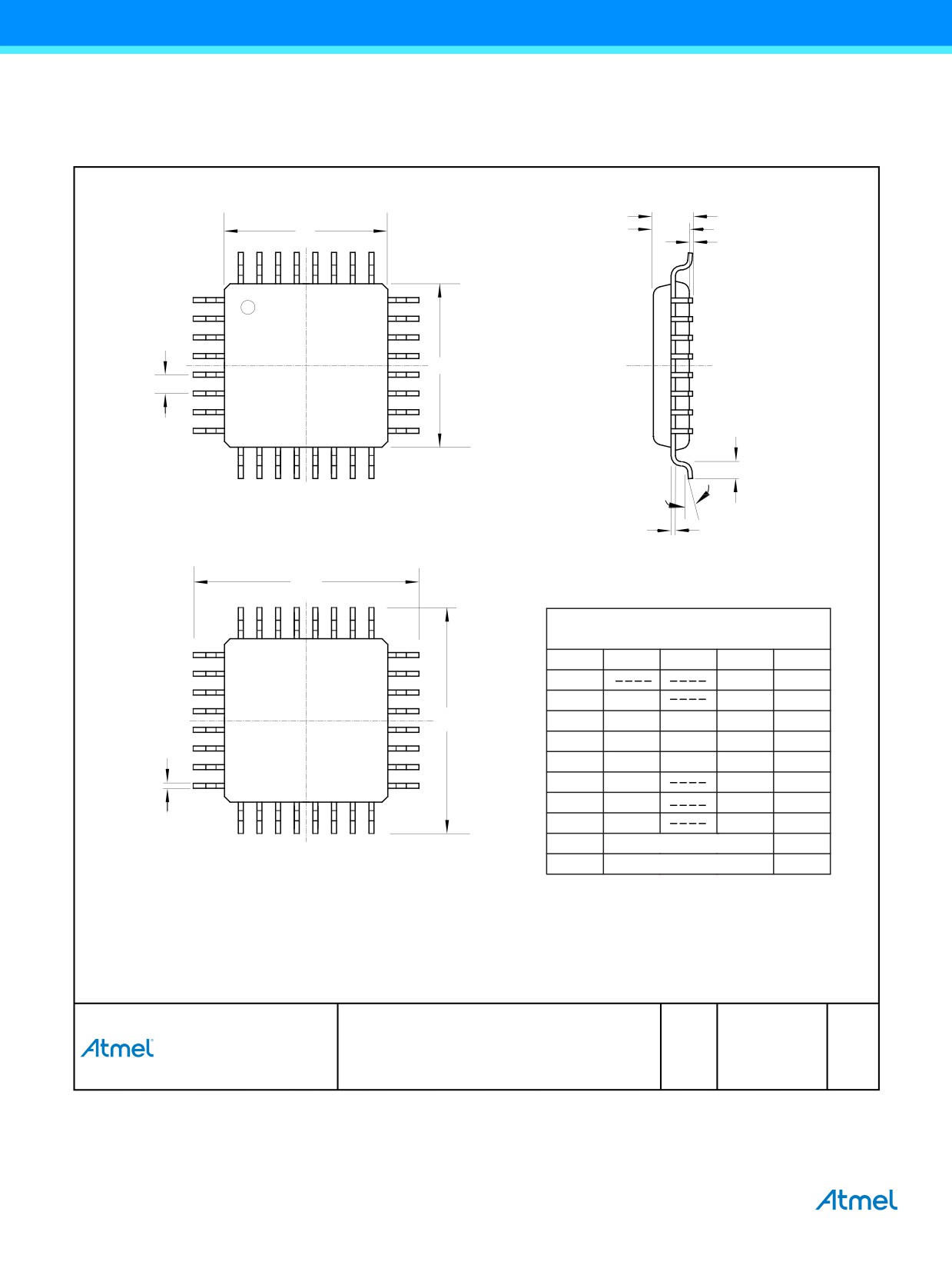
MA
Drawings not scaled
A
D1
A2
32
A1
1
E1
e
L
0°~7°
Top View
C
Side View
D
COMMON DIMENSIONS
(Unit of Measure = mm)
Symbol
MIN
NOM
MAX
NOTE
A
1.20
A1
0.05
0.15
E
A2
0.95
1.00
1.05
D/E
8.75
9.00
9.25
D1/E1
6.90
7.00
7.10
2
b
C
0.09
0.20
L
0.45
0.75
b
0.30
0.45
e
0.80 TYP.
Bottom View
n
32
Notes:
1.
This drawing is for general information only. Refer to JEDEC Drawing MS-026, Variation ABA.
2.
Dimensions D1 and E1 do not include mold protrusion. Allowable protrusion is 0.25mm per side.
Dimensions D1 and E1 are maximum plastic body size dimensions including mold mismatch.
3. Lead coplanarity is 0.10mm maximum.
02/29/12
TITLE
GPC
DRAWING NO.
REV.
Package Drawing Contact:
MA, 32 Lds - 0.80mm Pitch, 7x7x1.00mm Body size
Thin Profile Plastic Quad Flat Package (TQFP)
AUT
MA
C
packagedrawings@atmel.com
286
ATmega328P [DATASHEET]
7810D-AVR-01/15
33.2
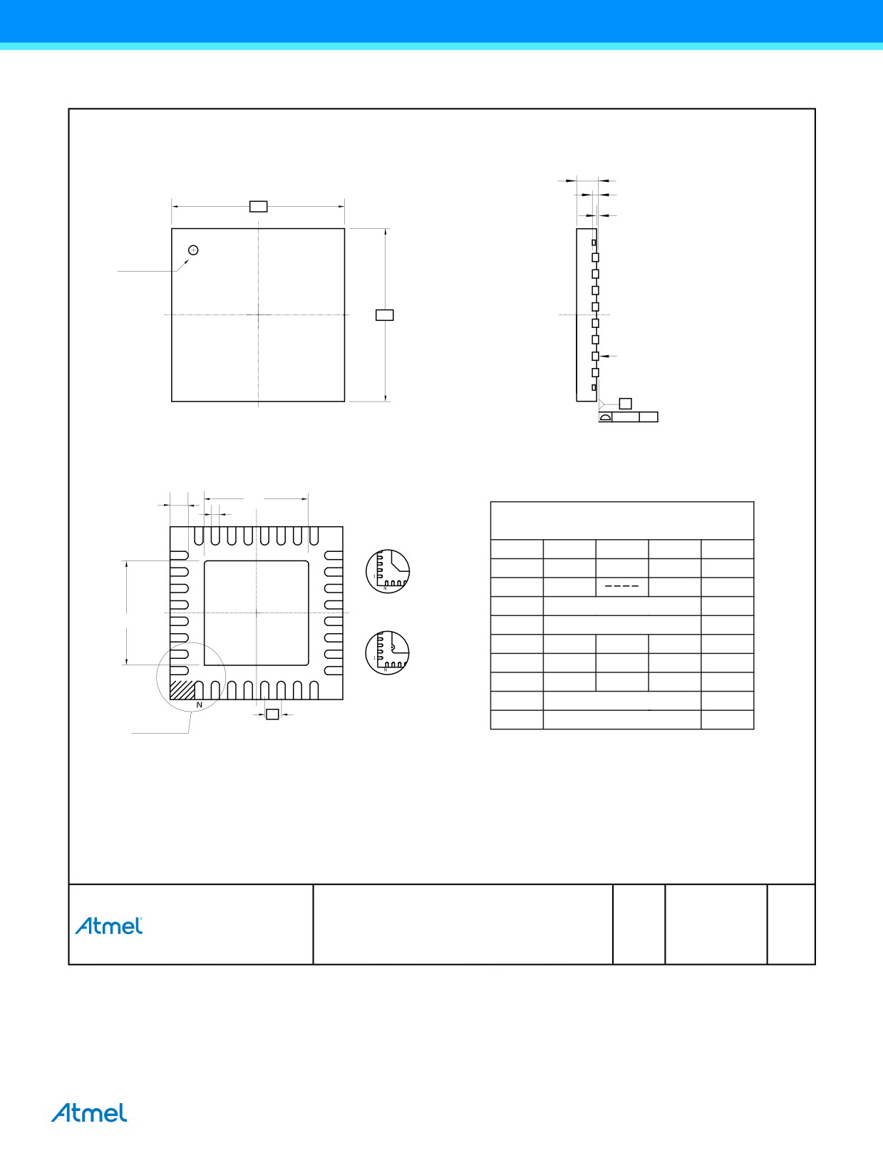
PN
Drawings not scaled
A
A3
D
N
A1
1
0.30
Dia. Typ. Laser Marking
E
Seating Plane
C
0.080
C
Top View
Side View
L
D2
b
COMMON DIMENSIONS
(Unit of Measure = mm)
Option A
Symbol
MIN
NOM
MAX
NOTE
A
0.80
0.85
0.90
A1
0.00
0.05
Pin 1# Chamfer
A3
0.20 REF
(C 0.30)
E2
Option B
D/E
5.00 BSC
PIN1 ID
D2/E2
3.00
3.10
3.20
L
0.30
0.40
0.50
1
Pin 1# Notch
b
0.18
0.25
0.30
2
(C 0.20 R)
e
0.50 BSC
See Options
e
n
32
A, B
Bottom View
Notes:
1.
This drawing is for general information only. Refer to JEDEC Drawing MO-220, Variation VHHD-2, for proper dimensions, tolerances, datums, etc.
2. Dimensions b applies to metallized terminal and is measured between 0.15mm and 0.30mm from the terminal tip.
If the terminal has the optical radius on the other end of the terminal, the dimensions should not be measured in that radius area.
01/31/12
TITLE
GPC
DRAWING NO.
REV.
Package Drawing Contact:
PN, 32 Leads - 0.50mm Pitch, 5x5mm
Very Thin Quad Flat no Lead Package (VQFN) Sawn
ZMF
PN
I
packagedrawings@atmel.com
ATmega328P [DATASHEET]
287
7810D-AVR-01/15
34.
Errata
34.1
Errata ATmega328P
The revision letter in this section refers to the revision of the Atmel® ATmega328P device.
34.1.1
Revision D
No known errata.
34.1.2
Revision A to Revision C
Not sampled.
35.
Revision History
Please note that the following page numbers referred to in this section refer to the specific revision mentioned, not to this
document.
Revision No.
History
7810D-AVR-01/15
Put datasheet in the latest template
7810C-AVR-10/12
ATmega88P and ATmega168P references removed
MA package updated
7810B-AVR-03/12
PN package updated
Creation of the automotive version starting from industrial version based on the
7810A-AVR-11/09
ATmega48P/88P/168P/328P datasheet 8025F-AVR-08/08. Temperature and voltage
ranges reflecting automotive requirements.
288
ATmega328P [DATASHEET]
7810D-AVR-01/15
36.
Table of Contents
Features
1
1.
Pin Configurations
3
1.1
Pin Descriptions
4
1.2
Disclaimer
5
1.3
Automotive Quality Grade
5
2.
Overview
6
2.1
Block Diagram
6
3.
Resources
8
4.
Data Retention
8
5.
About Code Examples
8
6.
AVR CPU Core
9
6.1
Overview
9
6.2
ALU - Arithmetic Logic Unit
10
6.3
Status Register
10
6.4
General Purpose Register File
12
6.5
Stack Pointer
13
6.6
Instruction Execution Timing
14
6.7
Reset and Interrupt Handling
15
7.
AVR Memories
17
7.1
Overview
17
7.2
In-System Reprogrammable Flash Program Memory
17
7.3
SRAM Data Memory
18
7.4
EEPROM Data Memory
19
7.5
I/O Memory
19
7.6
Register Description
20
8.
System Clock and Clock Options
24
8.1
Clock Systems and their Distribution
24
8.2
Clock Sources
25
8.3
Low Power Crystal Oscillator
26
8.4
Full Swing Crystal Oscillator
27
8.5
Low Frequency Crystal Oscillator
29
8.6
Calibrated Internal RC Oscillator
29
8.7
128 kHz Internal Oscillator
30
8.8
External Clock
31
8.9
Clock Output Buffer
31
8.10
Timer/Counter Oscillator
32
8.11
System Clock Prescaler
32
8.12
Register Description
32
ATmega328P [DATASHEET]
289
7810D-AVR-01/15
9.
Power Management and Sleep Modes
34
9.1
Sleep Modes
34
9.2
BOD Disable
35
9.3
Idle Mode
35
9.4
ADC Noise Reduction Mode
35
9.5
Power-down Mode
35
9.6
Power-save Mode
36
9.7
Standby Mode
36
9.8
Extended Standby Mode
36
9.9
Power Reduction Register
36
9.10
Minimizing Power Consumption
36
9.11
Register Description
37
10.
System Control and Reset
40
10.1
Resetting the AVR
40
10.2
Reset Sources
40
10.3
Power-on Reset
41
10.4
External Reset
42
10.5
Brown-out Detection
42
10.6
Watchdog System Reset
43
10.7
Internal Voltage Reference
43
10.8
Watchdog Timer
43
10.9
Register Description
46
11.
Interrupts
49
11.1
Interrupt Vectors in ATmega328P
49
11.2
Register Description
52
12.
External Interrupts
53
12.1
Pin Change Interrupt Timing
53
12.2
Register Description
54
13.
I/O-Ports
58
13.1
Overview
58
13.2
Ports as General Digital I/O
59
13.3
Alternate Port Functions
63
13.4
Register Description
72
14.
8-bit Timer/Counter0 with PWM
74
14.1
Features
74
14.2
Overview
74
14.3
Timer/Counter Clock Sources
75
14.4
Counter Unit
75
14.5
Output Compare Unit
76
14.6
Compare Match Output Unit
77
14.7
Modes of Operation
78
14.8
Timer/Counter Timing Diagrams
82
14.9
Register Description
84
290
ATmega328P [DATASHEET]
7810D-AVR-01/15
15.
16-bit Timer/Counter1 with PWM
89
15.1
Features
89
15.2
Overview
89
15.3
Accessing 16-bit Registers
91
15.4
Timer/Counter Clock Sources
94
15.5
Counter Unit
95
15.6
Input Capture Unit
95
15.7
Output Compare Units
97
15.8
Compare Match Output Unit
99
15.9
Modes of Operation
100
15.10
Timer/Counter Timing Diagrams
106
15.11
Register Description
108
16.
Timer/Counter0 and Timer/Counter1 Prescalers
114
16.1
Internal Clock Source
114
16.2
Prescaler Reset
114
16.3
External Clock Source
114
16.4
Register Description
115
17.
8-bit Timer/Counter2 with PWM and Asynchronous Operation
116
17.1
Features
116
17.2
Overview
116
17.3
Timer/Counter Clock Sources
117
17.4
Counter Unit
117
17.5
Output Compare Unit
118
17.6
Compare Match Output Unit
119
17.7
Modes of Operation
120
17.8
Timer/Counter Timing Diagrams
124
17.9
Asynchronous Operation of Timer/Counter2
126
17.10
Timer/Counter Prescaler
127
17.11
Register Description
127
18.
SPI - Serial Peripheral Interface
135
18.1
Features
135
18.2
Overview
135
18.3
SS Pin Functionality
138
18.4
Data Modes
139
18.5
Register Description
140
19.
USART0
143
19.1
Features
143
19.2
Overview
143
19.3
Clock Generation
144
19.4
Frame Formats
147
19.5
USART Initialization
148
19.6
Data Transmission - The USART Transmitter
150
19.7
Data Reception - The USART Receiver
152
19.8
Asynchronous Data Reception
155
19.9
Multi-processor Communication Mode
158
19.10
Register Description
159
19.11
Examples of Baud Rate Setting
163
ATmega328P [DATASHEET]
291
7810D-AVR-01/15
20.
USART in SPI Mode
166
20.1
Features
166
20.2
Overview
166
20.3
Clock Generation
166
20.4
SPI Data Modes and Timing
167
20.5
Frame Formats
167
20.6
Data Transfer
169
20.7
AVR USART MSPIM versus AVR SPI
170
20.8
Register Description
170
21.
2-wire Serial Interface
173
21.1
Features
173
21.2
2-wire Serial Interface Bus Definition
173
21.3
Data Transfer and Frame Format
174
21.4
Multi-master Bus Systems, Arbitration and Synchronization
177
21.5
Overview of the TWI Module
179
21.6
Using the TWI
181
21.7
Transmission Modes
184
21.8
Multi-master Systems and Arbitration
197
21.9
Register Description
198
22.
Analog Comparator
202
22.1
Overview
202
22.2
Analog Comparator Multiplexed Input
202
22.3
Register Description
203
23.
Analog-to-Digital Converter
205
23.1
Features
205
23.2
Overview
205
23.3
Starting a Conversion
207
23.4
Prescaling and Conversion Timing
208
23.5
Changing Channel or Reference Selection
211
23.6
ADC Noise Canceler
211
23.7
ADC Conversion Result
215
23.8
Temperature Measurement
215
23.9
Register Description
217
24.
debugWIRE On-chip Debug System
221
24.1
Features
221
24.2
Overview
221
24.3
Physical Interface
221
24.4
Software Break Points
222
24.5
Limitations of debugWIRE
222
24.6
Register Description
222
25.
Self-Programming the Flash, ATmega328P
223
25.1
Overview
223
25.2
Addressing the Flash During Self-Programming
224
25.3
Register Description’
228
292
ATmega328P [DATASHEET]
7810D-AVR-01/15
26.
Boot Loader Support - Read-While-Write Self-Programming
229
26.1
Features
229
26.2
Overview
229
26.3
Application and Boot Loader Flash Sections
229
26.4
Read-While-Write and No Read-While-Write Flash Sections
229
26.5
Boot Loader Lock Bits
231
26.6
Entering the Boot Loader Program
232
26.7
Addressing the Flash During Self-Programming
233
26.8
Self-Programming the Flash
234
26.9
Register Description
239
27.
Memory Programming
241
27.1
Program And Data Memory Lock Bits
241
27.2
Fuse Bits
242
27.3
Signature Bytes
244
27.4
Calibration Byte
244
27.5
Page Size
245
27.6
Parallel Programming Parameters, Pin Mapping, and Commands
245
27.7
Parallel Programming
247
27.8
Serial Downloading
254
28.
Electrical Characteristics
258
28.1
Absolute Maximum Ratings
258
28.2
DC Characteristics
258
28.3
DC Characteristics
260
28.4
Speed Grades
260
28.5
Clock Characteristics
260
28.6
System and Reset Characteristics
261
28.7
SPI Timing Characteristics
262
28.8
2-wire Serial Interface Characteristics
264
28.9
ADC Characteristics
265
28.10
Parallel Programming Characteristics
265
29.
Typical Characteristics
268
29.1
ATmega328P Typical Characteristics
268
30.
Register Summary
275
31.
Instruction Set Summary
281
32.
Ordering Information
285
32.1
ATmega328P
285
33.
Packaging Information
286
33.1
MA
286
33.2
PN
287
34.
Errata
288
34.1
Errata ATmega328P
288
35.
Revision History
288
36.
Table of Contents
289
ATmega328P [DATASHEET]
293
7810D-AVR-01/15