Atmel ATmega328P 8-bit AVR Microcontroller. DATASHEET (2015) - page 6
21.9.3
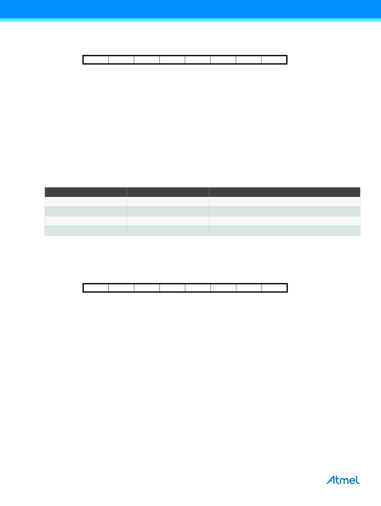
TWSR - TWI Status Register
Bit
7
6
5
4
3
2
1
0
(0xB9)
TWS7
TWS6
TWS5
TWS4
TWS3
-
TWPS1
TWPS0
TWSR
Read/Write
R
R
R
R
R
R
R/W
R/W
Initial Value
1
1
1
1
1
0
0
0
• Bits 7..3 - TWS: TWI Status
These 5 bits reflect the status of the TWI logic and the 2-wire serial bus. The different status codes are described later in this
section. Note that the value read from TWSR contains both the 5-bit status value and the 2-bit prescaler value. The
application designer should mask the prescaler bits to zero when checking the status bits. This makes status checking
independent of prescaler setting. This approach is used in this datasheet, unless otherwise noted.
• Bit 2 - Res: Reserved Bit
This bit is reserved and will always read as zero.
• Bits 1..0 - TWPS: TWI Prescaler Bits
These bits can be read and written, and control the bit rate prescaler.
Table 21-8. TWI Bit Rate Prescaler
TWPS1
TWPS0
Prescaler Value
0
0
1
0
1
4
1
0
16
1
1
64
To calculate bit rates, see Section 21.5.2 “Bit Rate Generator Unit” on page 180. The value of TWPS1..0 is used in the
equation.
21.9.4
TWDR - TWI Data Register
Bit
7
6
5
4
3
2
1
0
(0xBB)
TWD7
TWD6
TWD5
TWD4
TWD3
TWD2
TWD1
TWD0
TWDR
Read/Write
R/W
R/W
R/W
R/W
R/W
R/W
R/W
R/W
Initial Value
1
1
1
1
1
1
1
1
In transmit mode, TWDR contains the next byte to be transmitted. In receive mode, the TWDR contains the last byte
received. It is writable while the TWI is not in the process of shifting a byte. This occurs when the TWI interrupt flag (TWINT)
is set by hardware. Note that the data register cannot be initialized by the user before the first interrupt occurs. The data in
TWDR remains stable as long as TWINT is set. While data is shifted out, data on the bus is simultaneously shifted in. TWDR
always contains the last byte present on the bus, except after a wake up from a sleep mode by the TWI interrupt. In this
case, the contents of TWDR is undefined.
In the case of a lost bus arbitration, no data is lost in the transition from master to slave. Handling of the ACK bit is controlled
automatically by the TWI logic, the CPU cannot access the ACK bit directly.
• Bits 7..0 - TWD: TWI Data Register
These eight bits constitute the next data byte to be transmitted, or the latest data byte received on the 2-wire serial bus.
200
ATmega328P [DATASHEET]
7810D-AVR-01/15
21.9.5
TWAR - TWI (Slave) Address Register
Bit
7
6
5
4
3
2
1
0
(0xBA)
TWA6
TWA5
TWA4
TWA3
TWA2
TWA1
TWA0
TWGCE
TWAR
Read/Write
R/W
R/W
R/W
R/W
R/W
R/W
R/W
R/W
Initial Value
1
1
1
1
1
1
1
0
The TWAR should be loaded with the 7-bit slave address (in the seven most significant bits of TWAR) to which the TWI will
respond when programmed as a slave transmitter or receiver, and not needed in the master modes. In multi master
systems, TWAR must be set in masters which can be addressed as slaves by other masters.
The LSB of TWAR is used to enable recognition of the general call address (0x00). There is an associated address
comparator that looks for the slave address (or general call address if enabled) in the received serial address. If a match is
found, an interrupt request is generated.
• Bits 7..1 - TWA: TWI (Slave) Address Register
These seven bits constitute the slave address of the TWI unit.
• Bit 0 - TWGCE: TWI General Call Recognition Enable Bit
If set, this bit enables the recognition of a general call given over the 2-wire serial bus.
21.9.6
TWAMR - TWI (Slave) Address Mask Register
Bit
7
6
5
4
3
2
1
0
(0xBD)
TWAM[6:0]
-
TWAMR
Read/Write
R/W
R/W
R/W
R/W
R/W
R/W
R/W
R
Initial Value
0
0
0
0
0
0
0
0
• Bits 7..1 - TWAM: TWI Address Mask
The TWAMR can be loaded with a 7-bit slave address mask. Each of the bits in TWAMR can mask (disable) the
corresponding address bits in the TWI address register (TWAR). If the mask bit is set to one then the address match logic
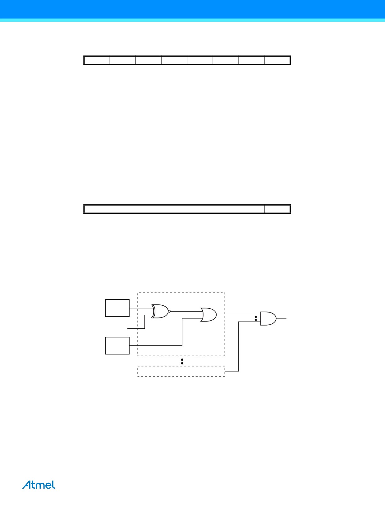
ignores the compare between the incoming address bit and the corresponding bit in TWAR. Figure 21-22 shown the address
match logic in detail.
Figure 21-22. TWI Address Match Logic, Block Diagram
TWAR0
Address
Match
Address
Bit 0
TWAMR0
Address Bit Comparator 0
Address Bit Comparator 6 to 1
• Bit 0 - Res: Reserved Bit
This bit is an unused bit in the ATmega328P, and will always read as zero.
ATmega328P [DATASHEET]
201
7810D-AVR-01/15
22.
Analog Comparator
22.1
Overview
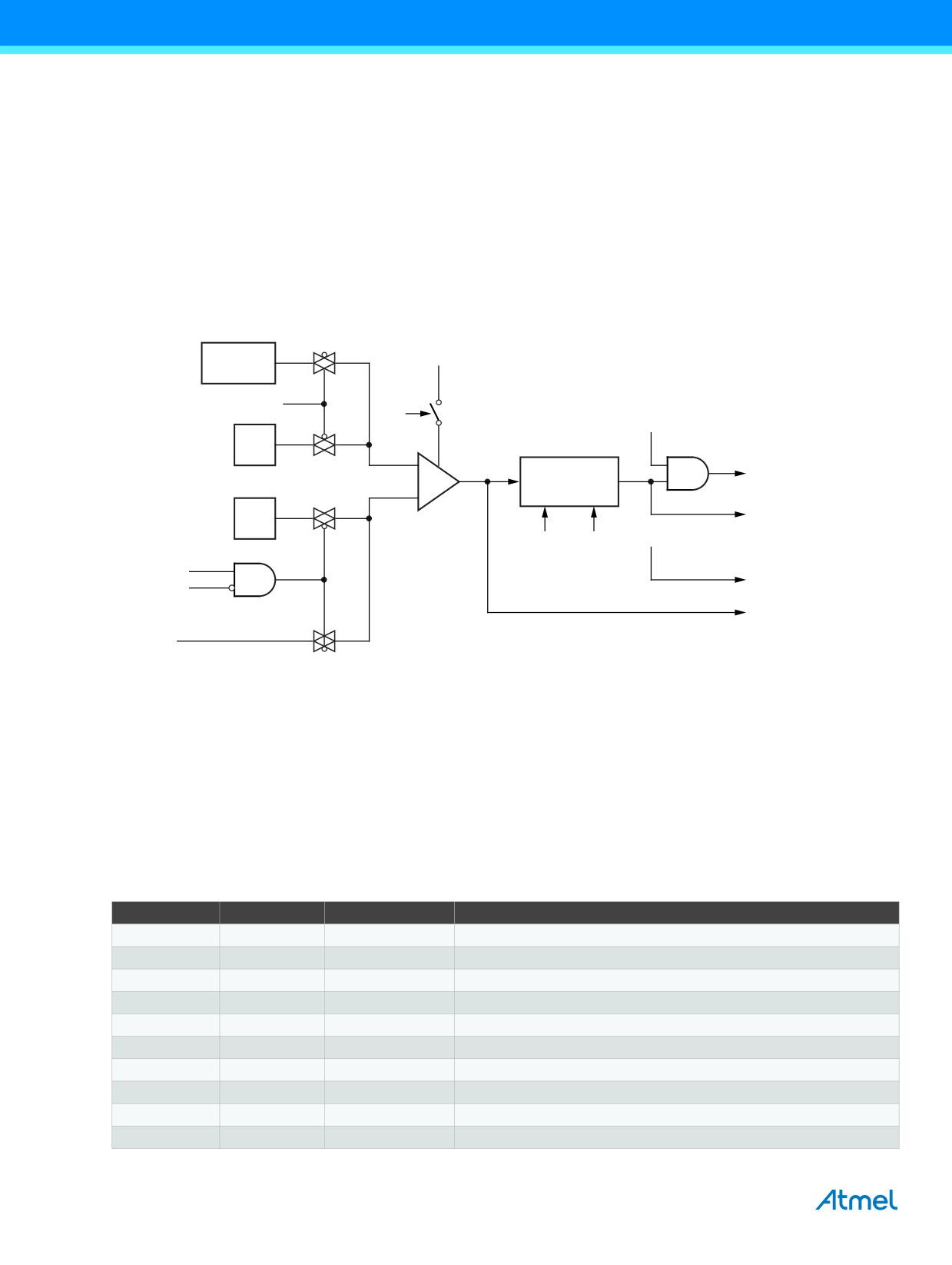
The analog comparator compares the input values on the positive pin AIN0 and negative pin AIN1. When the voltage on the
positive pin AIN0 is higher than the voltage on the negative pin AIN1, the analog comparator output, ACO, is set. The
comparator’s output can be set to trigger the Timer/Counter1 input capture function. In addition, the comparator can trigger a
separate interrupt, exclusive to the analog comparator. The user can select interrupt triggering on comparator output rise, fall
or toggle. A block diagram of the comparator and its surrounding logic is shown in Figure 22-1.
The power reduction ADC bit, PRADC, in Section 9.10 “Minimizing Power Consumption” on page 36 must be disabled by
writing a logical zero to be able to use the ADC input MUX.
Figure 22-1. Analog Comparator Block Diagram(2)
Bandgap
VCC
Reference
ACBG
ACD
ACIE
AIN0
Analog
+
Interrupt
Comparator
Select
IRQ
-
ACI
AIN1
ACIS1
ACIS0
ACIC
ACME
ADEN
To T/C1 Capture
ACO
Trigger MUX
ADC Multiplexer
Output(1)
Notes:
1.
See Table 22-1.
2.
Refer to Figure 1-1 on page 3 and Table 13-9 on page 70 for analog comparator pin placement.
22.2
Analog Comparator Multiplexed Input
It is possible to select any of the ADC7..0 pins to replace the negative input to the analog comparator. The ADC multiplexer
is used to select this input, and consequently, the ADC must be switched off to utilize this feature. If the analog comparator
multiplexer enable bit (ACME in ADCSRB) is set and the ADC is switched off (ADEN in ADCSRA is zero), MUX2..0 in
ADMUX select the input pin to replace the negative input to the analog comparator, as shown in Table 22-1. If ACME is
cleared or ADEN is set, AIN1 is applied to the negative input to the analog comparator.
Table 22-1. Analog Comparator Multiplexed Input
ACME
ADEN
MUX2..0
Analog Comparator Negative Input
0
x
xxx
AIN1
1
1
xxx
AIN1
1
0
000
ADC0
1
0
001
ADC1
1
0
010
ADC2
1
0
011
ADC3
1
0
100
ADC4
1
0
101
ADC5
1
0
110
ADC6
1
0
111
ADC7
202
ATmega328P [DATASHEET]
7810D-AVR-01/15
22.3
Register Description
22.3.1
ADCSRB - ADC Control and Status Register B
Bit
7
6
5
4
3
2
1
0
(0x7B)
-
ACME
-
-
-
ADTS2
ADTS1
ADTS0
ADCSRB
Read/Write
R
R/W
R
R
R
R/W
R/W
R/W
Initial Value
0
0
0
0
0
0
0
0
• Bit 6 - ACME: Analog Comparator Multiplexer Enable
When this bit is written logic one and the ADC is switched off (ADEN in ADCSRA is zero), the ADC multiplexer selects the
negative input to the Analog Comparator. When this bit is written logic zero, AIN1 is applied to the negative input of the
Analog Comparator. For a detailed description of this bit, see Section 22.2 “Analog Comparator Multiplexed Input” on page
202.
22.3.2
ACSR - Analog Comparator Control and Status Register
Bit
7
6
5
4
3
2
1
0
0x30 (0x50)
ACD
ACBG
ACO
ACI
ACIE
ACIC
ACIS1
ACIS0
ACSR
Read/Write
R/W
R/W
R
R/W
R/W
R/W
R/W
R/W
Initial Value
0
0
N/A
0
0
0
0
0
• Bit 7 - ACD: Analog Comparator Disable
When this bit is written logic one, the power to the analog comparator is switched off. This bit can be set at any time to turn
off the analog comparator. This will reduce power consumption in active and idle mode. When changing the ACD bit, the
analog comparator interrupt must be disabled by clearing the ACIE bit in ACSR. Otherwise an interrupt can occur when the
bit is changed.
• Bit 6 - ACBG: Analog Comparator Bandgap Select
When this bit is set, a fixed bandgap reference voltage replaces the positive input to the analog comparator. When this bit is
cleared, AIN0 is applied to the positive input of the analog comparator. When the bandgap referance is used as input to the
analog comparator, it will take a certain time for the voltage to stabilize. If not stabilized, the first conversion may give a
wrong value. See Section 10.7 “Internal Voltage Reference” on page 43
• Bit 5 - ACO: Analog Comparator Output
The output of the analog comparator is synchronized and then directly connected to ACO. The synchronization introduces a
delay of 1 - 2 clock cycles.
• Bit 4 - ACI: Analog Comparator Interrupt Flag
This bit is set by hardware when a comparator output event triggers the interrupt mode defined by ACIS1 and ACIS0. The
analog comparator interrupt routine is executed if the ACIE bit is set and the I-bit in SREG is set. ACI is cleared by hardware
when executing the corresponding interrupt handling vector. Alternatively, ACI is cleared by writing a logic one to the flag.
• Bit 3 - ACIE: Analog Comparator Interrupt Enable
When the ACIE bit is written logic one and the I-bit in the status register is set, the analog comparator interrupt is activated.
When written logic zero, the interrupt is disabled.
ATmega328P [DATASHEET]
203
7810D-AVR-01/15

• Bit 2 - ACIC: Analog Comparator Input Capture Enable
When written logic one, this bit enables the input capture function in Timer/Counter1 to be triggered by the analog
comparator. The comparator output is in this case directly connected to the input capture front-end logic, making the
comparator utilize the noise canceler and edge select features of the Timer/Counter1 input capture interrupt. When written
logic zero, no connection between the analog comparator and the input capture function exists. To make the comparator
trigger the Timer/Counter1 input capture interrupt, the ICIE1 bit in the timer interrupt mask register (TIMSK1) must be set.
• Bits 1, 0 - ACIS1, ACIS0: Analog Comparator Interrupt Mode Select
These bits determine which comparator events that trigger the analog comparator interrupt. The different settings are shown
in Table 22-2.
Table 22-2. ACIS1/ACIS0 Settings
ACIS1
ACIS0
Interrupt Mode
0
0
Comparator interrupt on output toggle.
0
1
Reserved
1
0
Comparator interrupt on falling output edge.
1
1
Comparator interrupt on rising output edge.
When changing the ACIS1/ACIS0 bits, the analog comparator interrupt must be disabled by clearing its interrupt enable bit in
the ACSR register. Otherwise an interrupt can occur when the bits are changed.
22.3.3
DIDR1 - Digital Input Disable Register 1
Bit
7
6
5
4
3
2
1
0
(0x7F)
-
-
-
-
-
-
AIN1D
AIN0D
DIDR1
Read/Write
R
R
R
R
R
R
R/W
R/W
Initial Value
0
0
0
0
0
0
0
0
• Bit 7..2 - Res: Reserved Bits
These bits are unused bits in the ATmega328P, and will always read as zero.
• Bit 1, 0 - AIN1D, AIN0D: AIN1, AIN0 Digital Input Disable
When this bit is written logic one, the digital input buffer on the AIN1/0 pin is disabled. The corresponding PIN register bit will
always read as zero when this bit is set. When an analog signal is applied to the AIN1/0 pin and the digital input from this pin
is not needed, this bit should be written logic one to reduce power consumption in the digital input buffer.
204
ATmega328P [DATASHEET]
7810D-AVR-01/15
23.
Analog-to-Digital Converter
23.1
Features
●
10-bit resolution
●
0.5 LSB integral non-linearity
●
±2 LSB absolute accuracy
●
65 to 260µs conversion time
● Up to 15kSPS
●
6 multiplexed single ended input channels
●
2 additional multiplexed single ended input channels
● Temperature sensor input channel
● Optional left adjustment for ADC result readout
●
0 to VCC ADC input voltage range
● Selectable 1.1V ADC reference voltage
● Free running or single conversion mode
● Interrupt on ADC conversion complete
● Sleep mode noise canceler
23.2
Overview
The Atmel® ATmega328P features a 10-bit successive approximation ADC. The ADC is connected to an 8-channel analog
multiplexer which allows eight single-ended voltage inputs constructed from the pins of Port A. The single-ended voltage
inputs refer to 0V (GND).
The ADC contains a sample and hold circuit which ensures that the input voltage to the ADC is held at a constant level
during conversion. A block diagram of the ADC is shown in Figure 23-1 on page 206.
The ADC has a separate analog supply voltage pin, AVCC. AVCC must not differ more than ±0.3V from VCC. See Section 23.6
“ADC Noise Canceler” on page 211 on how to connect this pin.
Internal reference voltages of nominally 1.1V or AVCC are provided on-chip. The voltage reference may be externally
decoupled at the AREF pin by a capacitor for better noise performance.
The power reduction ADC bit, PRADC, in Section 9.10 “Minimizing Power Consumption” on page 36 must be disabled by
writing a logical zero to enable the ADC.
The ADC converts an analog input voltage to a 10-bit digital value through successive approximation. The minimum value
represents GND and the maximum value represents the voltage on the AREF pin minus 1 LSB. Optionally, AVCC or an
internal 1.1V reference voltage may be connected to the AREF pin by writing to the REFSn bits in the ADMUX register. The
internal voltage reference may thus be decoupled by an external capacitor at the AREF pin to improve noise immunity.
ATmega328P [DATASHEET]
205
7810D-AVR-01/15
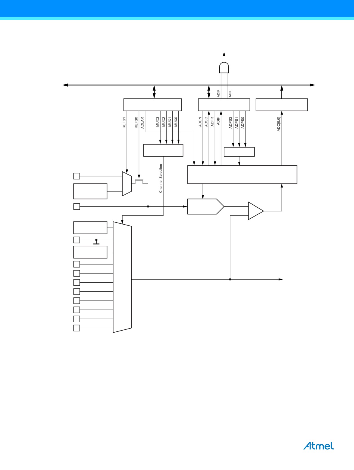
Figure 23-1. Analog to Digital Converter Block Schematic Operation
ADC Conversion
Complete IRQ
8-Bit Data Bus
15
0
ADC Multiplexer
ADC CTRL and Status
ADC Data Register
Select (ADMUX)
Register (ADCSRA)
(ADCH/ADCL)
MUX Decoder
Prescaler
Conversion Logic
AVCC
Internal 1.1V
Reference
Sample and Hold
Comparator
AREF
10-Bit DAC
-
+
Temperature
Sensor
GND
Bandgap
Reference
ADC7
ADC6
Input
ADC
MUX
Multiplexer
ADC5
Output
ADC4
ADC3
ADC2
ADC1
ADC0
The analog input channel is selected by writing to the MUX bits in ADMUX. Any of the ADC input pins, as well as GND and a
fixed bandgap voltage reference, can be selected as single ended inputs to the ADC. The ADC is enabled by setting the
ADC Enable bit, ADEN in ADCSRA. Voltage reference and input channel selections will not go into effect until ADEN is set.
The ADC does not consume power when ADEN is cleared, so it is recommended to switch off the ADC before entering
power saving sleep modes.
The ADC generates a 10-bit result which is presented in the ADC data registers, ADCH and ADCL. By default, the result is
presented right adjusted, but can optionally be presented left adjusted by setting the ADLAR bit in ADMUX.
If the result is left adjusted and no more than 8-bit precision is required, it is sufficient to read ADCH. Otherwise, ADCL must
be read first, then ADCH, to ensure that the content of the data registers belongs to the same conversion. Once ADCL is
read, ADC access to data registers is blocked.
206
ATmega328P [DATASHEET]
7810D-AVR-01/15
This means that if ADCL has been read, and a conversion completes before ADCH is read, neither register is updated and
the result from the conversion is lost. When ADCH is read, ADC access to the ADCH and ADCL registers is re-enabled.
The ADC has its own interrupt which can be triggered when a conversion completes. When ADC access to the data registers
is prohibited between reading of ADCH and ADCL, the interrupt will trigger even if the result is lost.
23.3
Starting a Conversion
A single conversion is started by disabling the power reduction ADC bit, PRADC, in Section 9.10 “Minimizing Power
Consumption” on page 36 by writing a logical zero to it and writing a logical one to the ADC start conversion bit, ADSC. This
bit stays high as long as the conversion is in progress and will be cleared by hardware when the conversion is completed. If
a different data channel is selected while a conversion is in progress, the ADC will finish the current conversion before
performing the channel change.
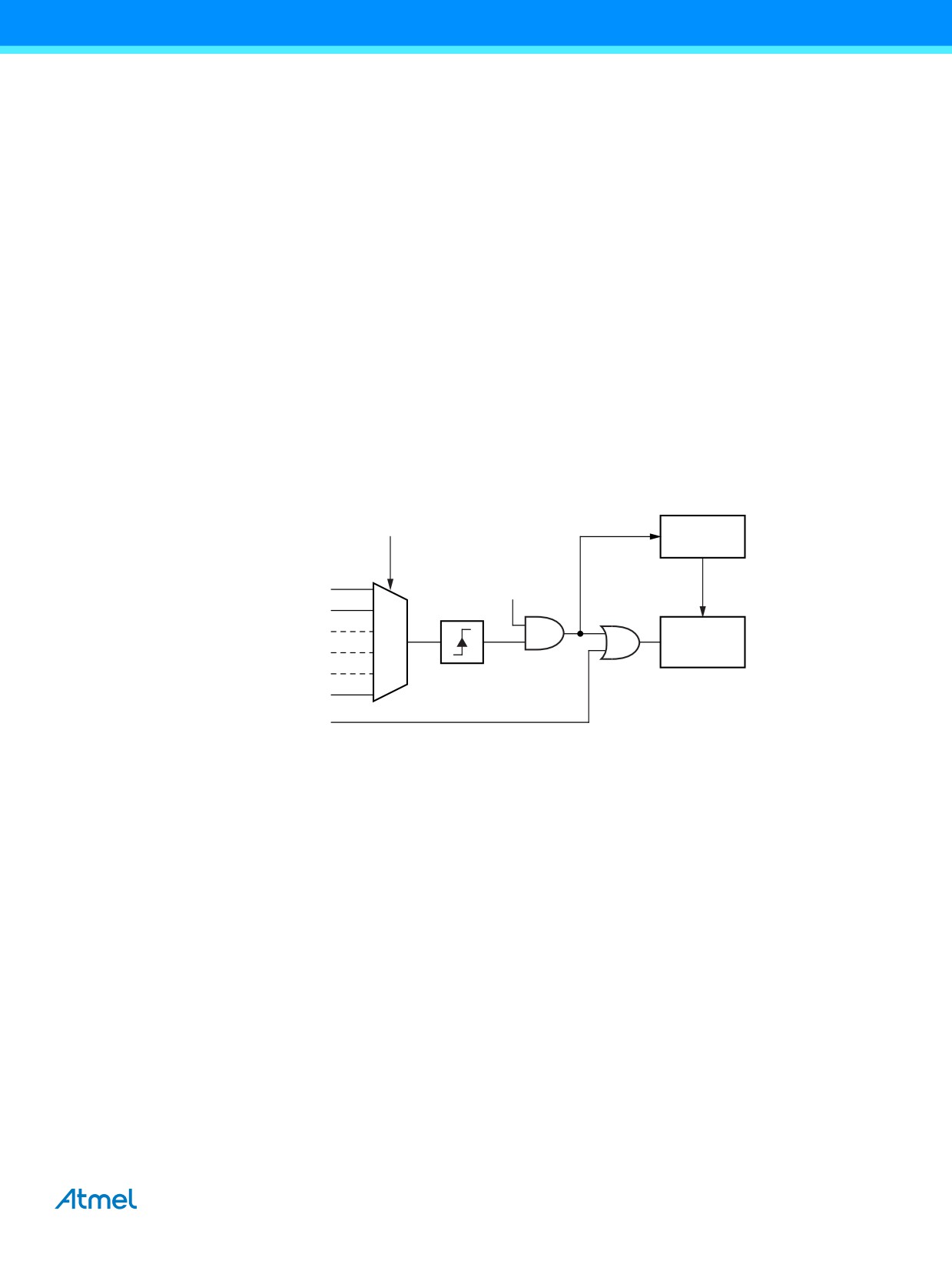
Alternatively, a conversion can be triggered automatically by various sources. Auto triggering is enabled by setting the ADC
auto trigger enable bit, ADATE in ADCSRA. The trigger source is selected by setting the ADC trigger select bits, ADTS in
ADCSRB (See description of the ADTS bits for a list of the trigger sources). When a positive edge occurs on the selected
trigger signal, the ADC prescaler is reset and a conversion is started. This provides a method of starting conversions at fixed
intervals. If the trigger signal still is set when the conversion completes, a new conversion will not be started. If another
positive edge occurs on the trigger signal during conversion, the edge will be ignored. Note that an interrupt flag will be set
even if the specific interrupt is disabled or the global interrupt enable bit in SREG is cleared. A conversion can thus be
triggered without causing an interrupt. However, the interrupt flag must be cleared in order to trigger a new conversion at the
next interrupt event.
Figure 23-2. ADC Auto Trigger Logic
ADTS[2:0]
Prescaler
START
CLKADC
ADIF
ADATE
SOURCE 1
Conversion
Logic
Edge
Detector
SOURCE n
ADSC
Using the ADC interrupt flag as a trigger source makes the ADC start a new conversion as soon as the ongoing conversion
has finished. The ADC then operates in free running mode, constantly sampling and updating the ADC data register. The
first conversion must be started by writing a logical one to the ADSC bit in ADCSRA. In this mode the ADC will perform
successive conversions independently of whether the ADC interrupt flag, ADIF is cleared or not.
If auto triggering is enabled, single conversions can be started by writing ADSC in ADCSRA to one. ADSC can also be used
to determine if a conversion is in progress. The ADSC bit will be read as one during a conversion, independently of how the
conversion was started.
ATmega328P [DATASHEET]
207
7810D-AVR-01/15
23.4
Prescaling and Conversion Timing
Figure 23-3. ADC Prescaler
ADEN
Reset
START
7-bit ADC Prescaler
CK
ADPS0
ADPS1
ADPS2
ADC Clock Source
By default, the successive approximation circuitry requires an input clock frequency between 50kHz and 200kHz to get
maximum resolution. If a lower resolution than 10 bits is needed, the input clock frequency to the ADC can be higher than
200kHz to get a higher sample rate.
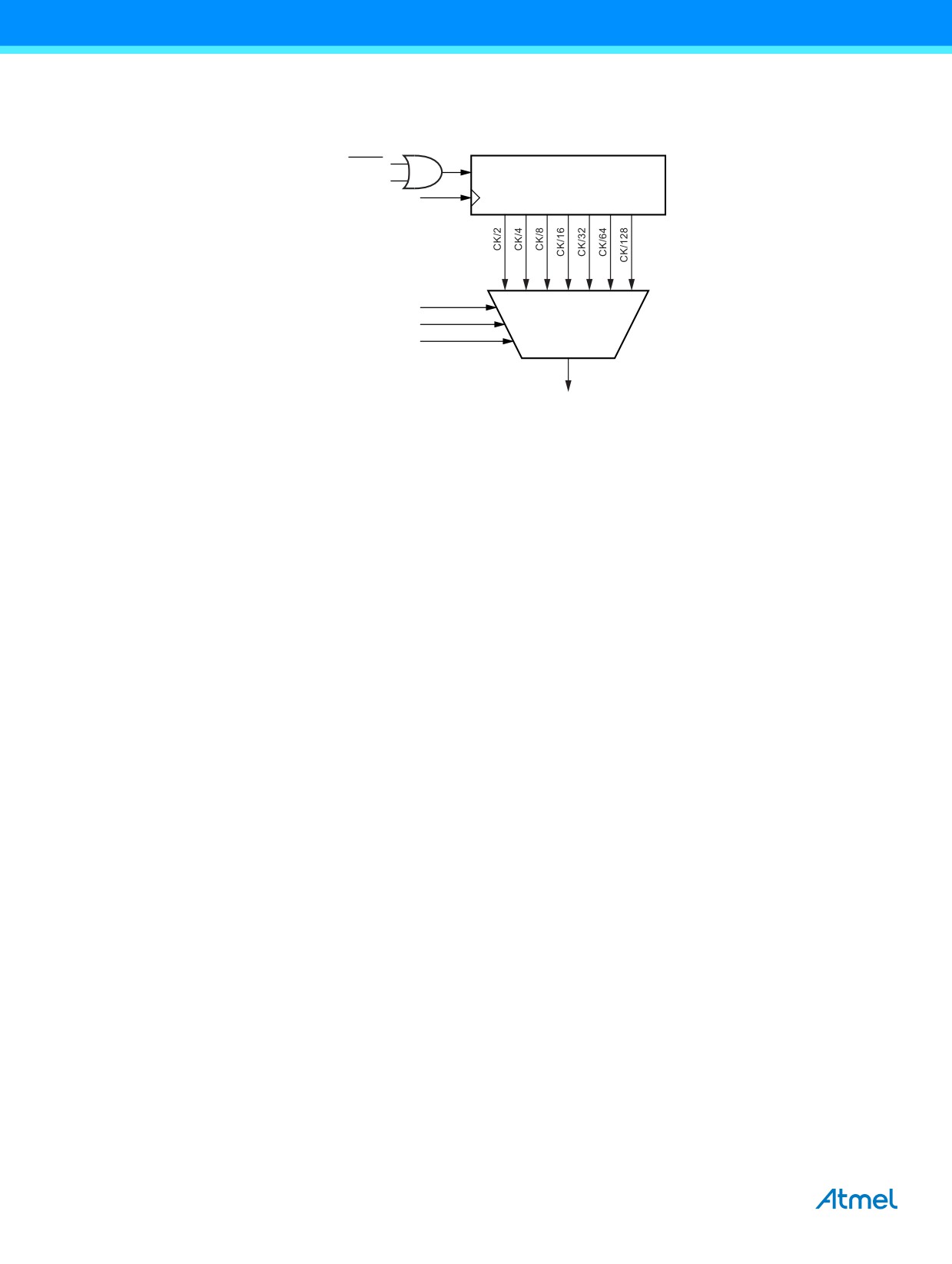
The ADC module contains a prescaler, which generates an acceptable ADC clock frequency from any CPU frequency above
100kHz. The prescaling is set by the ADPS bits in ADCSRA. The prescaler starts counting from the moment the ADC is
switched on by setting the ADEN bit in ADCSRA. The prescaler keeps running for as long as the ADEN bit is set, and is
continuously reset when ADEN is low.
When initiating a single ended conversion by setting the ADSC bit in ADCSRA, the conversion starts at the following rising
edge of the ADC clock cycle.
A normal conversion takes 13 ADC clock cycles. The first conversion after the ADC is switched on (ADEN in ADCSRA is set)
takes 25 ADC clock cycles in order to initialize the analog circuitry.
When the bandgap reference voltage is used as input to the ADC, it will take a certain time for the voltage to stabilize. If not
stabilized, the first value read after the first conversion may be wrong.
The actual sample-and-hold takes place 1.5 ADC clock cycles after the start of a normal conversion and 13.5 ADC clock
cycles after the start of an first conversion. When a conversion is complete, the result is written to the ADC data registers,
and ADIF is set. In single conversion mode, ADSC is cleared simultaneously. The software may then set ADSC again, and a
new conversion will be initiated on the first rising ADC clock edge.
When auto triggering is used, the prescaler is reset when the trigger event occurs. This assures a fixed delay from the trigger
event to the start of conversion. In this mode, the sample-and-hold takes place two ADC clock cycles after the rising edge on
the trigger source signal. Three additional CPU clock cycles are used for synchronization logic.
In free running mode, a new conversion will be started immediately after the conversion completes, while ADSC remains
high. For a summary of conversion times, see Table 23-1 on page 210.
208
ATmega328P [DATASHEET]
7810D-AVR-01/15
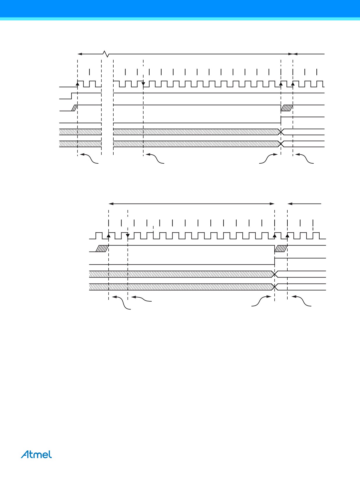
Figure 23-4. ADC Timing Diagram, First Conversion (Single Conversion Mode)
Next
First Conversion
Conversion
Cycle Number
1
2
12
13
14
15
16
17
18
19
20
21
22
23
24
25
1
2
3
ADC Clock
ADEN
ADSC
ADIF
ADCH
Sign and MSB of Result
ADCL
LSB of Result
MUX and REFS
Conversion
Sample and Hold
Update
Complete
MUX and REFS
Update
Figure 23-5. ADC Timing Diagram, Single Conversion
One Conversion
Next Conversion
Cycle Number
1
2
3
4
5
6
7
8
9
10
11
12
13
1
2
3
ADC Clock
ADSC
ADIF
ADCH
Sign and MSB of Result
ADCL
LSB of Result
Sample and Hold
Conversion
MUX and REFS
Complete
MUX and REFS
Update
Update
ATmega328P [DATASHEET]
209
7810D-AVR-01/15
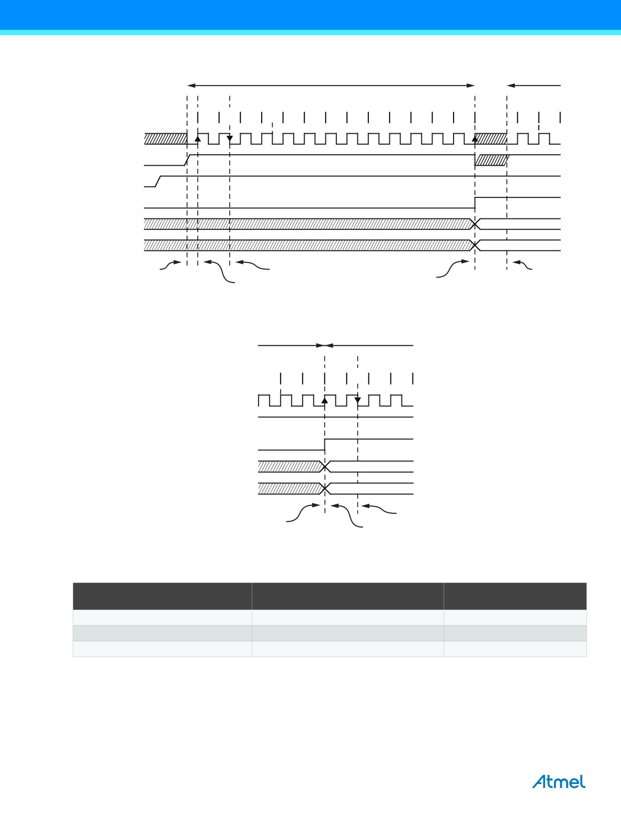
Figure 23-6. ADC Timing Diagram, Auto Triggered Conversion
One Conversion
Next Conversion
Cycle Number
1
2
3
4
5
6
7
8
9
10
11
12
13
1
2
ADC Clock
Trigger
Source
ADATE
ADIF
ADCH
Sign and MSB of Result
ADCL
LSB of Result
Sample and Hold
Prescaler
Prescaler
Conversion
MUX and REFS
Complete
Reset
Reset
Update
Figure 23-7. ADC Timing Diagram, Free Running Conversion
One Conversion
Next Conversion
Cycle Number
11
12
13
1
2
3
4
ADC Clock
ADSC
ADIF
ADCH
Sign and MSB of Result
ADCL
LSB of Result
Conversion
Sample and Hold
Complete
MUX and REFS
Update
Table 23-1. ADC Conversion Time
Sample and Hold
Condition
(Cycles from Start of Conversion)
Conversion Time (Cycles)
First conversion
13.5
25
Normal conversions, single ended
1.5
13
Auto triggered conversions
2
13.5
210
ATmega328P [DATASHEET]
7810D-AVR-01/15
23.5
Changing Channel or Reference Selection
The MUXn and REFS1:0 bits in the ADMUX register are single buffered through a temporary register to which the CPU has
random access. This ensures that the channels and reference selection only takes place at a safe point during the
conversion. The channel and reference selection is continuously updated until a conversion is started. Once the conversion
starts, the channel and reference selection is locked to ensure a sufficient sampling time for the ADC. Continuous updating
resumes in the last ADC clock cycle before the conversion completes (ADIF in ADCSRA is set). Note that the conversion
starts on the following rising ADC clock edge after ADSC is written. The user is thus advised not to write new channel or
reference selection values to ADMUX until one ADC clock cycle after ADSC is written.
If auto triggering is used, the exact time of the triggering event can be indeterministic. Special care must be taken when
updating the ADMUX register, in order to control which conversion will be affected by the new settings.
If both ADATE and ADEN is written to one, an interrupt event can occur at any time. If the ADMUX register is changed in this
period, the user cannot tell if the next conversion is based on the old or the new settings. ADMUX can be safely updated in
the following ways:
a. When ADATE or ADEN is cleared.
b. During conversion, minimum one ADC clock cycle after the trigger event.
c.
After a conversion, before the Interrupt Flag used as trigger source is cleared.
When updating ADMUX in one of these conditions, the new settings will affect the next ADC conversion.
23.5.1
ADC Input Channels
When changing channel selections, the user should observe the following guidelines to ensure that the correct channel is
selected:
In single conversion mode, always select the channel before starting the conversion. The channel selection may be changed
one ADC clock cycle after writing one to ADSC. However, the simplest method is to wait for the conversion to complete
before changing the channel selection.
In free running mode, always select the channel before starting the first conversion. The channel selection may be changed
one ADC clock cycle after writing one to ADSC. However, the simplest method is to wait for the first conversion to complete,
and then change the channel selection. Since the next conversion has already started automatically, the next result will
reflect the previous channel selection. Subsequent conversions will reflect the new channel selection.
23.5.2
ADC Voltage Reference
The reference voltage for the ADC (VREF) indicates the conversion range for the ADC. Single ended channels that exceed
VREF will result in codes close to 0x3FF. VREF can be selected as either AVCC, internal 1.1V reference, or external AREF pin.
AVCC is connected to the ADC through a passive switch. The internal 1.1V reference is generated from the internal bandgap
reference (VBG) through an internal amplifier. In either case, the external AREF pin is directly connected to the ADC, and the
reference voltage can be made more immune to noise by connecting a capacitor between the AREF pin and ground. VREF
can also be measured at the AREF pin with a high impedance voltmeter. Note that VREF is a high impedance source, and
only a capacitive load should be connected in a system.
If the user has a fixed voltage source connected to the AREF pin, the user may not use the other reference voltage options
in the application, as they will be shorted to the external voltage. If no external voltage is applied to the AREF pin, the user
may switch between AVCC and 1.1V as reference selection. The first ADC conversion result after switching reference voltage
source may be inaccurate, and the user is advised to discard this result.
23.6
ADC Noise Canceler
The ADC features a noise canceler that enables conversion during sleep mode to reduce noise induced from the CPU core
and other I/O peripherals. The noise canceler can be used with ADC noise reduction and idle mode. To make use of this
feature, the following procedure should be used:
a. Make sure that the ADC is enabled and is not busy converting. Single Conversion mode must be selected and the
ADC conversion complete interrupt must be enabled.
b. Enter ADC Noise Reduction mode (or Idle mode). The ADC will start a conversion once the CPU has been halted.
ATmega328P [DATASHEET]
211
7810D-AVR-01/15
c.
If no other interrupts occur before the ADC conversion completes, the ADC interrupt will wake up the CPU and
execute the ADC Conversion Complete interrupt routine. If another interrupt wakes up the CPU before the ADC
conversion is complete, that interrupt will be executed, and an ADC Conversion Complete interrupt request will be
generated when the ADC conversion completes. The CPU will remain in active mode until a new sleep command
is executed.
Note that the ADC will not be automatically turned off when entering other sleep modes than idle mode and ADC noise
reduction mode. The user is advised to write zero to ADEN before entering such sleep modes to avoid excessive power
consumption.
23.6.1
Analog Input Circuitry
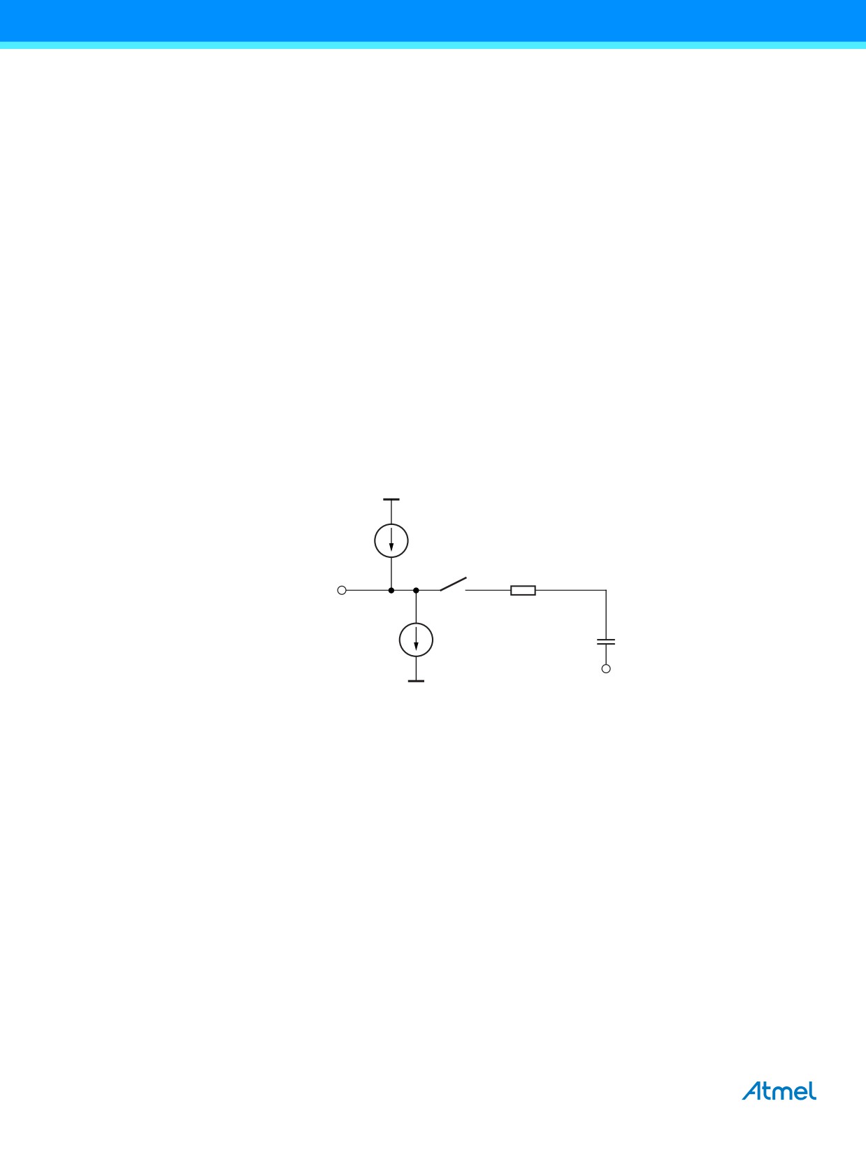
The analog input circuitry for single ended channels is illustrated in Figure 23-8 on page 212 An analog source applied to
ADCn is subjected to the pin capacitance and input leakage of that pin, regardless of whether that channel is selected as
input for the ADC. When the channel is selected, the source must drive the S/H capacitor through the series resistance
(combined resistance in the input path).
The ADC is optimized for analog signals with an output impedance of approximately 10k or less. If such a source is used,
the sampling time will be negligible. If a source with higher impedance is used, the sampling time will depend on how long
time the source needs to charge the S/H capacitor, with can vary widely. The user is recommended to only use low
impedance sources with slowly varying signals, since this minimizes the required charge transfer to the S/H capacitor.
Signal components higher than the nyquist frequency (fADC/2) should not be present for either kind of channels, to avoid
distortion from unpredictable signal convolution. The user is advised to remove high frequency components with a low-pass
filter before applying the signals as inputs to the ADC.
Figure 23-8. Analog Input Circuitry
IIH
ADCn
1 to 100kΩ
IIL
CS/H = 14pF
VCC/2
23.6.2
Analog Noise Canceling Techniques
Digital circuitry inside and outside the device generates EMI which might affect the accuracy of analog measurements. If
conversion accuracy is critical, the noise level can be reduced by applying the following techniques:
a. Keep analog signal paths as short as possible. Make sure analog tracks run over the analog ground plane, and
keep them well away from high-speed switching digital tracks.
b. The AVCC pin on the device should be connected to the digital VCC supply voltage via an LC network as shown in
Figure 23-9 on page 213.
c.
Use the ADC noise canceler function to reduce induced noise from the CPU.
d. If any ADC [3..0] port pins are used as digital outputs, it is essential that these do not switch while a
conversion is in progress. However, using the 2-wire interface (ADC4 and ADC5) will only affect the
conversion on ADC4 and ADC5 and not the other ADC channels.
212
ATmega328P [DATASHEET]
7810D-AVR-01/15
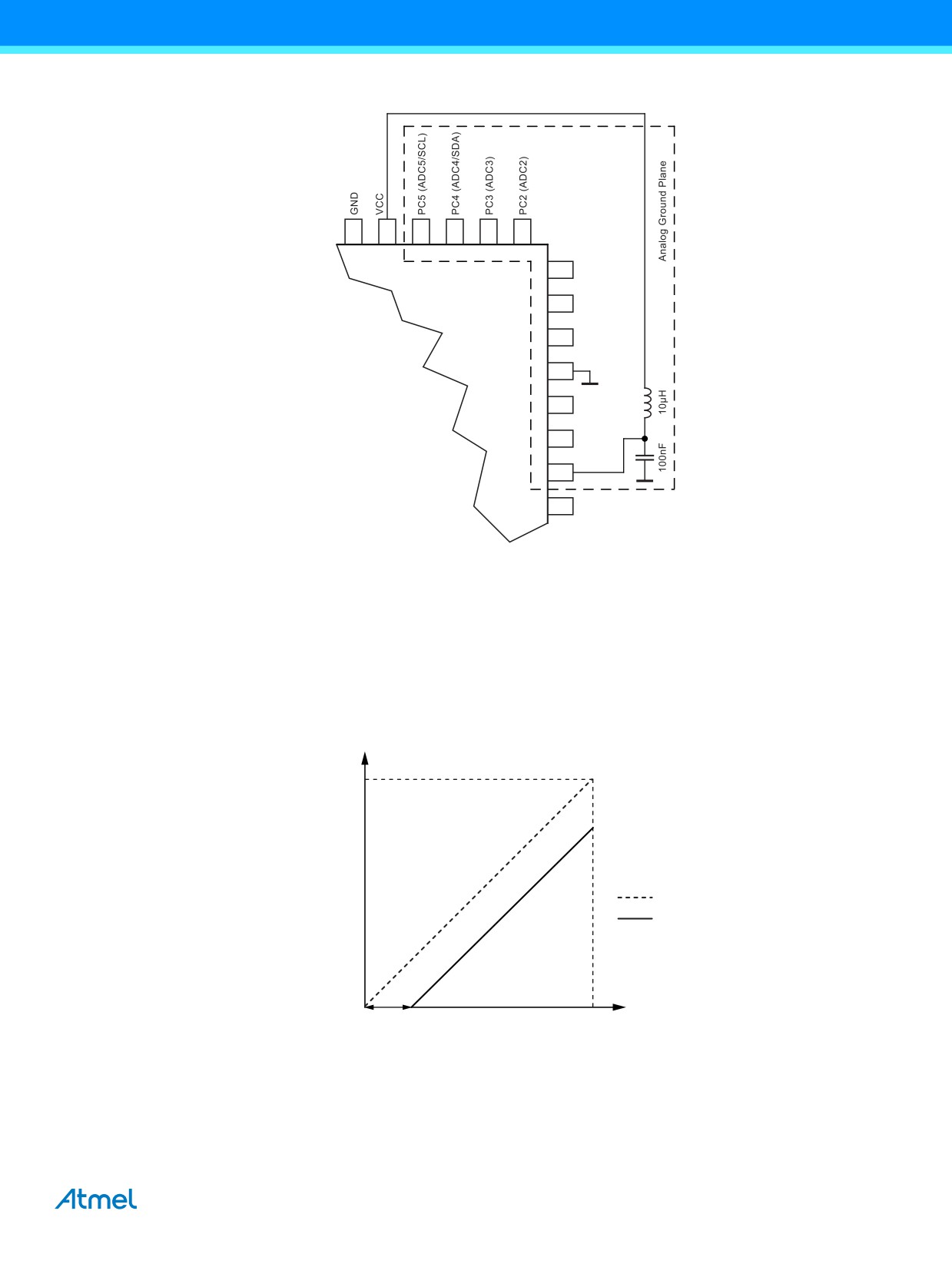
Figure 23-9. ADC Power Connections
PC1 (ADC1)
PC0 (ADC0)
ADC7
GND
AREF
ADC6
AVCC
PB5
23.6.3
ADC Accuracy Definitions
An n-bit single-ended ADC converts a voltage linearly between GND and VREF in 2n steps (LSBs). The lowest code is read
as 0, and the highest code is read as 2n-1.
Several parameters describe the deviation from the ideal behavior:
● Offset: The deviation of the first transition (0x000 to 0x001) compared to the ideal transition (at 0.5 LSB). Ideal value:
0 LSB.
Figure 23-10. Offset Error
Output Code
Ideal ADC
Actual ADC
Offset
Error
VREF
Input Voltage
ATmega328P [DATASHEET]
213
7810D-AVR-01/15
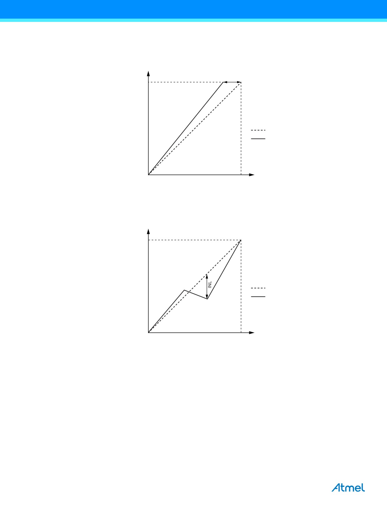
● Gain error: After adjusting for offset, the gain error is found as the deviation of the last transition (0x3FE to 0x3FF)
compared to the ideal transition (at 1.5 LSB below maximum). Ideal value: 0 LSB
Figure 23-11. Gain Error
Output Code
Gain
Error
Ideal ADC
Actual ADC
VREF
Input Voltage
● Integral non-linearity (INL): After adjusting for offset and gain error, the INL is the maximum deviation of an actual
transition compared to an ideal transition for any code. Ideal value: 0 LSB.
Figure 23-12. Integral Non-linearity (INL)
Output Code
Ideal ADC
Actual ADC
VREF
Input Voltage
214
ATmega328P [DATASHEET]
7810D-AVR-01/15
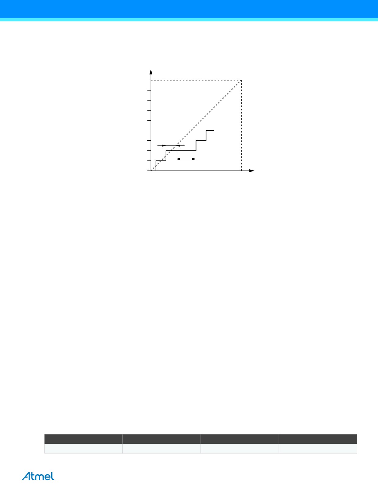
● Differential non-linearity (DNL): The maximum deviation of the actual code width (the interval between two adjacent
transitions) from the ideal code width (1 LSB). Ideal value: 0 LSB.
Figure 23-13. Differential Non-linearity (DNL)
Output Code
0x3FF
1 LSB
DNL
0x000
0
VREF
Input Voltage
● Quantization error: Due to the quantization of the input voltage into a finite number of codes, a range of input voltages
(1 LSB wide) will code to the same value. Always ±0.5 LSB.
● Absolute accuracy: The maximum deviation of an actual (unadjusted) transition compared to an ideal transition for
any code. This is the compound effect of offset, gain error, differential error, non-linearity, and quantization error. Ideal
value: ±0.5 LSB.
23.7
ADC Conversion Result
After the conversion is complete (ADIF is high), the conversion result can be found in the ADC result registers (ADCL,
ADCH).
For single ended conversion, the result is:
VIN 1024
ADC
= ---------------------------
V
REF
where VIN is the voltage on the selected input pin and VREF the selected voltage reference (see Table 23-3 on page 217 and
Table 23-4 on page 218). 0x000 represents analog ground, and 0x3FF represents the selected reference voltage minus one
LSB.
23.8
Temperature Measurement
The temperature measurement is based on an on-chip temperature sensor that is coupled to a single ended ADC input.
MUX[4..0] bits in ADMUX register enables the temperature sensor. The internal 1.1V voltage reference must also be
selected for the ADC voltage reference source in the temperature sensor measurement. When the temperature sensor is
enabled, the ADC converter can be used in single conversion mode to measure the voltage over the temperature sensor.
The measured voltage has a linear relationship to the temperature as described in Table 23-2 on page 215.
The voltage sensitivity is approximately 1LSB/°C and the accuracy of the temperature measurement is ±10°C using
manufacturing calibration values (TS_GAIN, TS_OFFSET).
The values described in Table 23-2 are typical values. However, due to the process variation the temperature sensor output
varies from one chip to another.
Table 23-2. Sensor Output Code versus Temperature (Typical Values)
Temperature/°C
-40°C
+25°C
+125°C
0x010D
0x0160
0x01E0
ATmega328P [DATASHEET]
215
7810D-AVR-01/15
23.8.1
Manufacturing Calibration
Calibration values determined during test are available in the signature row.
The temperature in degrees celsius can be calculated using the formula:
ADCH<<8 + ADCL - 273 + 100 - TS_OFFSET 128
+ 25
TS_GAIN
Where:.
a. ADCH and ADCL are the ADC data registers,
b. is the temperature sensor gain
c.
TS_OFFSET is the temperature sensor offset correction term
TS_GAIN is the unsigned fixed point 8-bit temperature sensor gain factor in
1/128th units stored in the signature row.
TS_OFFSET is the signed twos complement temperature sensor offset reading
stored in the signature row. See Table 26-5 on page 236 for signature row parameter address
The following code example allows to read signature row data
.equ TS_GAIN = 0x0003
.equ TS_OFFSET = 0x0002
LDI R30,LOW(TS_GAIN)
LDI R31,HIGH (TS_GAIN)
RCALL Read_signature_row
MOV R17,R16; Save R16 result
LDI R30,LOW(TS_OFFSET)
LDI R31,HIGH (TS_OFFSET)
RCALL Read_signature_row
; R16 holds TS_OFFSET and R17 holds TS_GAIN
Read_signature_row:
IN R16,SPMCSR; Wait for SPMEN ready
SBRC R16,SPMEN; Exit loop here when SPMCSR is free
RJMP Read_signature_row
LDI R16,((1<<SIGRD)|(1<<SPMEN)); We need to set SIGRD and SPMEN together
OUT SPMCSR,R16; and execute the LPM within 3 cycles
LPM R16,Z
RET
216
ATmega328P [DATASHEET]
7810D-AVR-01/15

23.9
Register Description
23.9.1
ADMUX - ADC Multiplexer Selection Register
Bit
7
6
5
4
3
2
1
0
(0x7C)
REFS1
REFS0
ADLAR
-
MUX3
MUX2
MUX1
MUX0
ADMUX
Read/Write
R/W
R/W
R/W
R
R/W
R/W
R/W
R/W
Initial Value
0
0
0
0
0
0
0
0
• Bit 7:6 - REFS1:0: Reference Selection Bits
These bits select the voltage reference for the ADC, as shown in Table 23-3. If these bits are changed during a conversion,
the change will not go in effect until this conversion is complete (ADIF in ADCSRA is set). The internal voltage reference
options may not be used if an external reference voltage is being applied to the AREF pin.
Table 23-3. Voltage Reference Selections for ADC
REFS1
REFS0
Voltage Reference Selection
0
0
AREF, internal VREF turned off
0
1
AVCC with external capacitor at AREF pin
1
0
Reserved
1
1
Internal 1.1V voltage reference with external capacitor at AREF pin
• Bit 5 - ADLAR: ADC Left Adjust Result
The ADLAR bit affects the presentation of the ADC conversion result in the ADC data register. Write one to ADLAR to left
adjust the result. Otherwise, the result is right adjusted. Changing the ADLAR bit will affect the ADC data register
immediately, regardless of any ongoing conversions. For a complete description of this bit, see Section 23.9.3 “ADCL and
ADCH - The ADC Data Register” on page 219.
• Bit 4 - Res: Reserved Bit
This bit is an unused bit in the Atmel® ATmega328P, and will always read as zero.
• Bits 3:0 - MUX3:0: Analog Channel Selection Bits
The value of these bits selects which analog inputs are connected to the ADC. See Table 23-4 on page 218 for details. If
these bits are changed during a conversion, the change will not go in effect until this conversion is complete (ADIF in
ADCSRA is set).
ATmega328P [DATASHEET]
217
7810D-AVR-01/15

Table 23-4. Input Channel Selections
MUX3..0
Single Ended Input
0000
ADC0
0001
ADC1
0010
ADC2
0011
ADC3
0100
ADC4
0101
ADC5
0110
ADC6
0111
ADC7
1000
ADC8(1)
1001
(reserved)
1010
(reserved)
1011
(reserved)
1100
(reserved)
1101
(reserved)
1110
1.1V (VBG)
1111
0V (GND)
Note:
1.
For temperature sensor.
23.9.2
ADCSRA - ADC Control and Status Register A
Bit
7
6
5
4
3
2
1
0
(0x7A)
ADEN
ADSC
ADATE
ADIF
ADIE
ADPS2
ADPS1
ADPS0
ADCSRA
Read/Write
R/W
R/W
R/W
R/W
R/W
R/W
R/W
R/W
Initial Value
0
0
0
0
0
0
0
0
• Bit 7 - ADEN: ADC Enable
Writing this bit to one enables the ADC. By writing it to zero, the ADC is turned off. Turning the ADC off while a conversion is
in progress, will terminate this conversion.
• Bit 6 - ADSC: ADC Start Conversion
In single conversion mode, write this bit to one to start each conversion. In free running mode, write this bit to one to start the
first conversion. The first conversion after ADSC has been written after the ADC has been enabled, or if ADSC is written at
the same time as the ADC is enabled, will take 25 ADC clock cycles instead of the normal 13. This first conversion performs
initialization of the ADC.
ADSC will read as one as long as a conversion is in progress. When the conversion is complete, it returns to zero. Writing
zero to this bit has no effect.
• Bit 5 - ADATE: ADC Auto Trigger Enable
When this bit is written to one, auto triggering of the ADC is enabled. The ADC will start a conversion on a positive edge of
the selected trigger signal. The trigger source is selected by setting the ADC trigger select bits, ADTS in ADCSRB.
• Bit 4 - ADIF: ADC Interrupt Flag
This bit is set when an ADC conversion completes and the data registers are updated. The ADC conversion complete
interrupt is executed if the ADIE bit and the I-bit in SREG are set. ADIF is cleared by hardware when executing the
corresponding interrupt handling vector. Alternatively, ADIF is cleared by writing a logical one to the flag. Beware that if
doing a read-modify-write on ADCSRA, a pending interrupt can be disabled. This also applies if the SBI and CBI instructions
are used.
218
ATmega328P [DATASHEET]
7810D-AVR-01/15
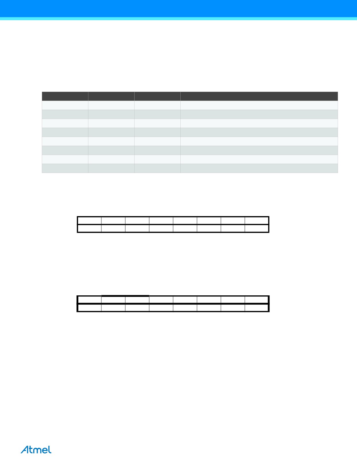
• Bit 3 - ADIE: ADC Interrupt Enable
When this bit is written to one and the I-bit in SREG is set, the ADC conversion complete interrupt is activated.
• Bits 2:0 - ADPS2:0: ADC Prescaler Select Bits
These bits determine the division factor between the system clock frequency and the input clock to the ADC.
Table 23-5. ADC Prescaler Selections
ADPS2
ADPS1
ADPS0
Division Factor
0
0
0
2
0
0
1
2
0
1
0
4
0
1
1
8
1
0
0
16
1
0
1
32
1
1
0
64
1
1
1
128
23.9.3
ADCL and ADCH - The ADC Data Register
23.9.3.1
ADLAR = 0
Bit
15
14
13
12
11
10
9
8
(0x79)
-
-
-
-
-
-
ADC9
ADC8
ADCH
(0x78)
ADC7
ADC6
ADC5
ADC4
ADC3
ADC2
ADC1
ADC0
ADCL
7
6
5
4
3
2
1
0
Read/Write
R
R
R
R
R
R
R
R
R
R
R
R
R
R
R
R
Initial Value
0
0
0
0
0
0
0
0
0
0
0
0
0
0
0
0
23.9.3.2
ADLAR = 1
Bit
15
14
13
12
11
10
9
8
(0x79)
ADC9
ADC8
ADC7
ADC6
ADC5
ADC4
ADC3
ADC2
ADCH
(0x78)
ADC1
ADC0
-
-
-
-
-
-
ADCL
7
6
5
4
3
2
1
0
Read/Write
R
R
R
R
R
R
R
R
R
R
R
R
R
R
R
R
Initial Value
0
0
0
0
0
0
0
0
0
0
0
0
0
0
0
0
When an ADC conversion is complete, the result is found in these two registers.
When ADCL is read, the ADC data register is not updated until ADCH is read. Consequently, if the result is left adjusted and
no more than 8-bit precision is required, it is sufficient to read ADCH. Otherwise, ADCL must be read first, then ADCH.
The ADLAR bit in ADMUX, and the MUXn bits in ADMUX affect the way the result is read from the registers. If ADLAR is set,
the result is left adjusted. If ADLAR is cleared (default), the result is right adjusted.
• ADC9:0: ADC Conversion Result
These bits represent the result from the conversion, as detailed in Section 23.7 “ADC Conversion Result” on page 215.
ATmega328P [DATASHEET]
219
7810D-AVR-01/15
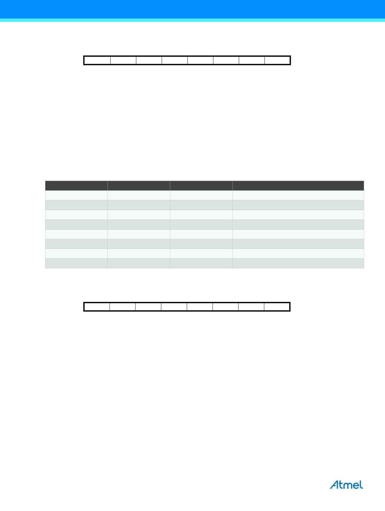
23.9.4
ADCSRB - ADC Control and Status Register B
Bit
7
6
5
4
3
2
1
0
(0x7B)
-
ACME
-
-
-
ADTS2
ADTS1
ADTS0
ADCSRB
Read/Write
R
R/W
R
R
R
R/W
R/W
R/W
Initial Value
0
0
0
0
0
0
0
0
• Bit 7, 5:3 - Res: Reserved Bits
These bits are reserved for future use. To ensure compatibility with future devices, these bits must be written to zero when
ADCSRB is written.
• Bit 2:0 - ADTS2:0: ADC Auto Trigger Source
If ADATE in ADCSRA is written to one, the value of these bits selects which source will trigger an ADC conversion. If ADATE
is cleared, the ADTS2:0 settings will have no effect. A conversion will be triggered by the rising edge of the selected interrupt
flag. Note that switching from a trigger source that is cleared to a trigger source that is set, will generate a positive edge on
the trigger signal. If ADEN in ADCSRA is set, this will start a conversion. Switching to free running mode (ADTS[2:0]=0) will
not cause a trigger event, even if the ADC interrupt flag is set.
Table 23-6. ADC Auto Trigger Source Selections
ADTS2
ADTS1
ADTS0
Trigger Source
0
0
0
Free running mode
0
0
1
Analog comparator
0
1
0
External interrupt request 0
0
1
1
Timer/Counter0 compare match A
1
0
0
Timer/Counter0 overflow
1
0
1
Timer/Counter1 compare match B
1
1
0
Timer/Counter1 overflow
1
1
1
Timer/Counter1 capture event
23.9.5
DIDR0 - Digital Input Disable Register 0
Bit
7
6
5
4
3
2
1
0
(0x7E)
-
-
ADC5D
ADC4D
ADC3D
ADC2D
ADC1D
ADC0D
DIDR0
Read/Write
R
R
R/W
R/W
R/W
R/W
R/W
R/W
Initial Value
0
0
0
0
0
0
0
0
• Bits 7:6 - Res: Reserved Bits
These bits are reserved for future use. To ensure compatibility with future devices, these bits must be written to zero when
DIDR0 is written.
• Bit 5:0 - ADC5D..ADC0D: ADC5..0 Digital Input Disable
When this bit is written logic one, the digital input buffer on the corresponding ADC pin is disabled. The corresponding PIN
register bit will always read as zero when this bit is set. When an analog signal is applied to the ADC5..0 pin and the digital
input from this pin is not needed, this bit should be written logic one to reduce power consumption in the digital input buffer.
Note that ADC pins ADC7 and ADC6 do not have digital input buffers, and therefore do not require digital input disable bits.
220
ATmega328P [DATASHEET]
7810D-AVR-01/15
24.
debugWIRE On-chip Debug System
24.1
Features
● Complete program flow control
● Emulates all on-chip functions, both digital and analog, except RESET pin
● Real-time operation
● Symbolic debugging support (both at C and assembler source level, or for other HLLs)
● Unlimited number of program break points (using software break points)
● Non-intrusive operation
● Electrical characteristics identical to real device
● Automatic configuration system
● High-speed operation
● Programming of non-volatile memories
24.2
Overview
The debugWIRE on-chip debug system uses a one-wire, bi-directional interface to control the program flow, execute AVR®
instructions in the CPU and to program the different non-volatile memories.
24.3
Physical Interface
When the debugWIRE enable (DWEN) fuse is programmed and lock bits are unprogrammed, the debugWIRE system within
the target device is activated. The RESET port pin is configured as a wire-AND (open-drain) bi-directional I/O pin with pull-up
enabled and becomes the communication gateway between target and emulator.
Figure 24-1. The debugWIRE Setup
1.8 - 5.5V
VCC
dw
dw(RESET)
GND
Figure 24-1 shows the schematic of a target MCU, with debugWIRE enabled, and the emulator connector. The system clock
is not affected by debugWIRE and will always be the clock source selected by the CKSEL fuses.
When designing a system where debugWIRE will be used, the following observations must be made for correct operation:
● Pull-up resistors on the dW/(RESET) line must not be smaller than 10k. The pull-up resistor is not required for
debugWIRE functionality.
● Connecting the RESET pin directly to VCC will not work.
● Capacitors connected to the RESET pin must be disconnected when using debugWire.
● All external reset sources must be disconnected.
ATmega328P [DATASHEET]
221
7810D-AVR-01/15
24.4
Software Break Points
debugWIRE supports program memory break points by the AVR® break instruction. Setting a Break Point in AVR Studio®
will insert a BREAK instruction in the program memory. The instruction replaced by the BREAK instruction will be stored.
When program execution is continued, the stored instruction will be executed before continuing from the program memory.
A break can be inserted manually by putting the BREAK instruction in the program.
The flash must be re-programmed each time a break point is changed. This is automatically handled by AVR Studio through
the debugWIRE interface. The use of break points will therefore reduce the flash data retention. Devices used for debugging
purposes should not be shipped to end customers.
24.5
Limitations of debugWIRE
The debugWIRE communication pin (dW) is physically located on the same pin as external reset (RESET). An external reset
source is therefore not supported when the debugWIRE is enabled.
A programmed DWEN fuse enables some parts of the clock system to be running in all sleep modes. This will increase the
power consumption while in sleep. Thus, the DWEN fuse should be disabled when debugWire is not used.
24.6
Register Description
The following section describes the registers used with the debugWire.
24.6.1
DWDR - debugWire Data Register
Bit
7
6
5
4
3
2
1
0
DWDR[7:0]
DWDR
Read/Write
R/W
R/W
R/W
R/W
R/W
R/W
R/W
R/W
Initial Value
0
0
0
0
0
0
0
0
The DWDR register provides a communication channel from the running program in the MCU to the debugger. This register
is only accessible by the debugWIRE and can therefore not be used as a general purpose register in the normal operations.
222
ATmega328P [DATASHEET]
7810D-AVR-01/15
25.
Self-Programming the Flash, ATmega328P
25.1
Overview
In Atmel® ATmega328P, there is no read-while-write support, and no separate boot loader section. The SPM instruction can
be executed from the entire flash.
The device provides a self-programming mechanism for downloading and uploading program code by the MCU itself. The
self-programming can use any available data interface and associated protocol to read code and write (program) that code
into the program memory.
The program memory is updated in a page by page fashion. Before programming a page with the data stored in the
temporary page buffer, the page must be erased. The temporary page buffer is filled one word at a time using SPM and the
buffer can be filled either before the page erase command or between a page erase and a page write operation:
Alternative 1, fill the buffer before a page erase
● Fill temporary page buffer
● Perform a page erase
● Perform a page write
Alternative 2, fill the buffer after page erase
● Perform a page erase
● Fill temporary page buffer
● Perform a page write
If only a part of the page needs to be changed, the rest of the page must be stored (for example in the temporary page
buffer) before the erase, and then be re-written. When using alternative 1, the boot loader provides an effective read-modify-
write feature which allows the user software to first read the page, do the necessary changes, and then write back the
modified data. If alternative 2 is used, it is not possible to read the old data while loading since the page is already erased.
The temporary page buffer can be accessed in a random sequence. It is essential that the page address used in both the
page erase and page write operation is addressing the same page.
25.1.1
Performing Page Erase by SPM
To execute page erase, set up the address in the Z-pointer, write “00000011” to SPMCSR and execute SPM within four
clock cycles after writing SPMCSR. The data in R1 and R0 is ignored. The page address must be written to PCPAGE in the
Z-register. Other bits in the Z-pointer will be ignored during this operation.
● The CPU is halted during the page erase operation.
25.1.2
Filling the Temporary Buffer (Page Loading)
To write an instruction word, set up the address in the Z-pointer and data in R1:R0, write “00000001” to SPMCSR and
execute SPM within four clock cycles after writing SPMCSR. The content of PCWORD in the Z-register is used to address
the data in the temporary buffer. The temporary buffer will auto-erase after a page write operation or by writing the
RWWSRE bit in SPMCSR. It is also erased after a system reset. Note that it is not possible to write more than one time to
each address without erasing the temporary buffer. If the EEPROM is written in the middle of an SPM page load operation,
all data loaded will be lost.
25.1.3
Performing a Page Write
To execute page write, set up the address in the Z-pointer, write “00000101” to SPMCSR and execute SPM within four clock
cycles after writing SPMCSR. The data in R1 and R0 is ignored. The page address must be written to PCPAGE. Other bits
in the Z-pointer must be written to zero during this operation.
● The CPU is halted during the page write operation.
ATmega328P [DATASHEET]
223
7810D-AVR-01/15
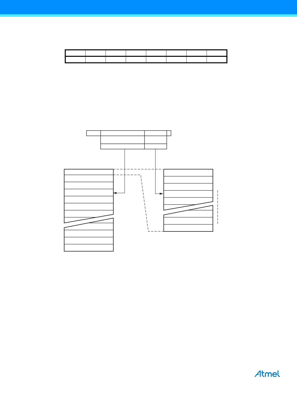
25.2
Addressing the Flash During Self-Programming
The Z-pointer is used to address the SPM commands.
Bit
15
14
13
12
11
10
9
8
ZH (R31)
Z15
Z14
Z13
Z12
Z11
Z10
Z9
Z8
ZL (R30)
Z7
Z6
Z5
Z4
Z3
Z2
Z1
Z0
7
6
5
4
3
2
1
0
Since the flash is organized in pages (see Table 27-9 on page 245), the program counter can be treated as having two
different sections. One section, consisting of the least significant bits, is addressing the words within a page, while the most
significant bits are addressing the pages. This is shown in Figure 26-3 on page 233. Note that the page erase and page write
operations are addressed independently. Therefore it is of major importance that the software addresses the same page in
both the page erase and page write operation.
The LPM instruction uses the Z-pointer to store the address. Since this instruction addresses the flash byte-by-byte, also the
LSB (bit Z0) of the Z-pointer is used.
Figure 25-1. Addressing the Flash During SPM(1)
Bit
15
ZPCMSB
ZPAGEMSB
1 0
Z-register
0
PCMSB
PAGEMSB
Program
PCPAGE
PCWORD
Counter
Page Address
Word Address
within the Flash
within a Page
Program Memory
Page
PCWORD[PAGEMSB:0]
Page
Instruction Word
00
01
02
PAGEEND
Note:
1.
The different variables used in Figure 26-3 on page 233 are listed in Table 27-9 on page 245.
25.2.1
EEPROM Write Prevents Writing to SPMCSR
Note that an EEPROM write operation will block all software programming to flash. Reading the fuses and lock bits from
software will also be prevented during the EEPROM write operation. It is recommended that the user checks the status bit
(EEPE) in the EECR register and verifies that the bit is cleared before writing to the SPMCSR register.
224
ATmega328P [DATASHEET]
7810D-AVR-01/15
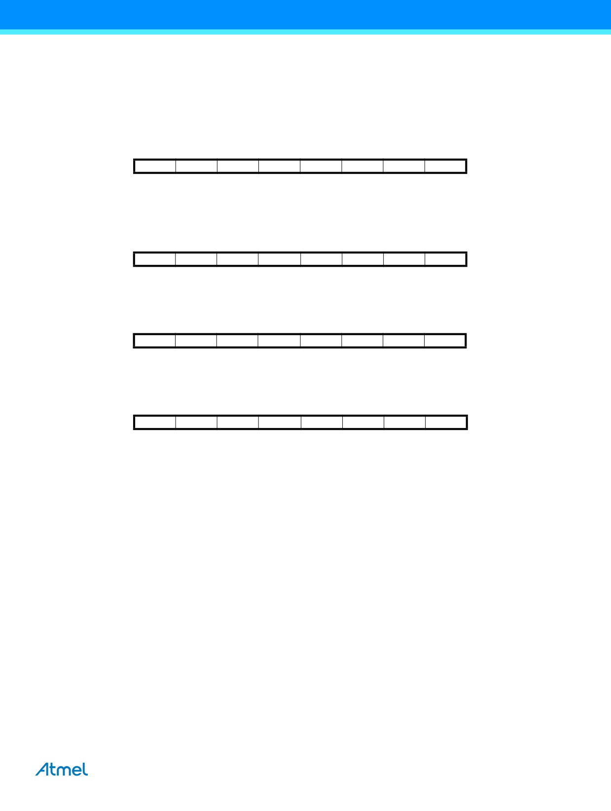
25.2.2
Reading the Fuse and Lock Bits from Software
It is possible to read both the fuse and lock bits from software. To read the lock bits, load the Z-pointer with 0x0001 and set
the BLBSET and SELFPRGEN bits in SPMCSR. When an LPM instruction is executed within three CPU cycles after the
BLBSET and SELFPRGEN bits are set in SPMCSR, the value of the Lock bits will be loaded in the destination register. The
BLBSET and SELFPRGEN bits will auto-clear upon completion of reading the lock bits or if no LPM instruction is executed
within three CPU cycles or no SPM instruction is executed within four CPU cycles. When BLBSET and SELFPRGEN are
cleared, LPM will work as described in the Instruction set manual.
Bit
7
6
5
4
3
2
1
0
Rd
-
-
-
-
-
-
LB2
LB1
The algorithm for reading the fuse low byte is similar to the one described above for reading the lock bits. To read the fuse
low byte, load the Z-pointer with 0x0000 and set the BLBSET and SELFPRGEN bits in SPMCSR. When an LPM instruction
is executed within three cycles after the BLBSET and SELFPRGEN bits are set in the SPMCSR, the value of the fuse low
byte (FLB) will be loaded in the destination register as shown below.See Table 27-5 on page 243 for a detailed description
and mapping of the fuse low byte.
Bit
7
6
5
4
3
2
1
0
Rd
FLB7
FLB6
FLB5
FLB4
FLB3
FLB2
FLB1
FLB0
Similarly, when reading the fuse high byte (FHB), load 0x0003 in the Z-pointer. When an LPM instruction is executed within
three cycles after the BLBSET and SELFPRGEN bits are set in the SPMCSR, the value of the fuse high byte will be loaded
in the destination register as shown below. See Table 27-4 on page 242 for detailed description and mapping of the
extended fuse byte.
Bit
7
6
5
4
3
2
1
0
Rd
FHB7
FHB6
FHB5
FHB4
FHB3
FHB2
FHB1
FHB0
Similarly, when reading the extended fuse byte (EFB), load 0x0002 in the Z-pointer. When an LPM instruction is executed
within three cycles after the BLBSET and SELFPRGEN bits are set in the SPMCSR, the value of the extended fuse byte will
be loaded in the destination register as shown below. See Table 27-5 on page 243 for detailed description and mapping of
the extended fuse byte.
Bit
7
6
5
4
3
2
1
0
Rd
FHB7
FHB6
FHB5
FHB4
FHB3
FHB2
FHB1
FHB0
Fuse and lock bits that are programmed, will be read as zero. Fuse and lock bits that are unprogrammed, will be read as
one.
25.2.3
Preventing Flash Corruption
During periods of low VCC, the flash program can be corrupted because the supply voltage is too low for the CPU and the
flash to operate properly. These issues are the same as for board level systems using the flash, and the same design
solutions should be applied.
A flash program corruption can be caused by two situations when the voltage is too low. First, a regular write sequence to
the flash requires a minimum voltage to operate correctly. Secondly, the CPU itself can execute instructions incorrectly, if the
supply voltage for executing instructions is too low.
Flash corruption can easily be avoided by following these design recommendations (one is sufficient):
1.
Keep the AVR RESET active (low) during periods of insufficient power supply voltage. This can be done by
enabling the internal brown-out detector (BOD) if the operating voltage matches the detection level. If not, an
external low VCC reset protection circuit can be used. If a reset occurs while a write operation is in progress, the
write operation will be completed provided that the power supply voltage is sufficient.
2.
Keep the AVR® core in power-down sleep mode during periods of low VCC. This will prevent the CPU from
attempting to decode and execute instructions, effectively protecting the SPMCSR register and thus the flash from
unintentional writes.
ATmega328P [DATASHEET]
225
7810D-AVR-01/15
25.2.4
Programming Time for Flash when Using SPM
The calibrated RC oscillator is used to time flash accesses. Table 26-6 on page 237 shows the typical programming time for
flash accesses from the CPU.
Table 25-1. SPM Programming Time(1)
Symbol
Min Programming Time
Max Programming Time
Flash write (page erase, page write, and write lock
3.7ms
4.5ms
bits by SPM)
Note:
1.
Minimum and maximum programming time is per individual operation.
25.2.5
Simple Assembly Code Example for a Boot Loader
Note that the RWWSB bit will always be read as zero in Atmel® ATmega328P. Nevertheless, it is recommended to check
this bit as shown in the code example, to ensure compatibility with devices supporting read-while-write.
;-the routine writes one page of data from RAM to Flash
; the first data location in RAM is pointed to by the Y pointer
; the first data location in Flash is pointed to by the Z-pointer
;-error handling is not included
;-the routine must be placed inside the Boot space
; (at least the Do_spm sub routine). Only code inside NRWW section can
; be read during Self-Programming (Page Erase and Page Write).
;-registers used: r0, r1, temp1 (r16), temp2 (r17), looplo (r24),
; loophi (r25), spmcrval (r20)
; storing and restoring of registers is not included in the routine
; register usage can be optimized at the expense of code size
;-It is assumed that either the interrupt table is moved to the Boot
; loader section or that the interrupts are disabled.
.equ
PAGESIZEB = PAGESIZE*2
;PAGESIZEB is page size in BYTES, not words
.org SMALLBOOTSTART
Write_page:
;Page Erase
ldi
spmcrval, (1<<PGERS) | (1<<SELFPRGEN)
rcall
Do_spm
;re-enable the RWW section
ldi
spmcrval, (1<<RWWSRE) | (1<<SELFPRGEN)
rcall
Do_spm
;transfer data from RAM to Flash page buffer
ldi
looplo, low(PAGESIZEB)
;init loop variable
ldi
loophi, high(PAGESIZEB)
;not required for PAGESIZEB<=256
Wrloop:
ld
r0, Y+
ld
r1, Y+
ldi
spmcrval, (1<<SELFPRGEN)
rcall
Do_spm
adiw
ZH:ZL, 2
sbiw
loophi:looplo, 2
;use subi for PAGESIZEB<=256
brne
Wrloop
;execute Page Write
subi
ZL, low(PAGESIZEB)
;restore pointer
sbci
ZH, high(PAGESIZEB)
;not required for PAGESIZEB<=256
ldi
spmcrval, (1<<PGWRT) | (1<<SELFPRGEN)
rcall
Do_spm
;re-enable the RWW section
ldi
spmcrval, (1<<RWWSRE) | (1<<SELFPRGEN)
226
ATmega328P [DATASHEET]
7810D-AVR-01/15
rcall Do_spm
;read back and check, optional
ldi
looplo, low(PAGESIZEB)
;init loop variable
ldi
loophi, high(PAGESIZEB)
;not required for PAGESIZEB<=256
subi
YL, low(PAGESIZEB)
;restore pointer
sbci
YH, high(PAGESIZEB)
Rdloop:
lpm
r0, Z+
ld
r1, Y+
cpse
r0, r1
rjmp
Error
sbiw
loophi:looplo, 1
;use subi for PAGESIZEB<=256
brne
Rdloop
;return to RWW section
;verify that RWW section is safe to read
Return:
in
temp1, SPMCSR
sbrs
temp1, RWWSB
; If RWWSB is set, the RWW section is not ready yet
ret
;re-enable the RWW section
ldi
spmcrval, (1<<RWWSRE) | (1<<SELFPRGEN)
rcall
Do_spm
rjmp
Return
Do_spm:
;check for previous SPM complete
Wait_spm:
in
temp1, SPMCSR
sbrc
temp1, SELFPRGEN
rjmp
Wait_spm
;input: spmcrval determines SPM action
;disable interrupts if enabled, store status
in
temp2, SREG
cli
;check that no EEPROM write access is present
Wait_ee:
sbic
EECR, EEPE
rjmp
Wait_ee
;SPM timed sequence
out
SPMCSR, spmcrval
spm
;restore SREG (to enable interrupts if originally enabled)
out
SREG, temp2
ret
ATmega328P [DATASHEET]
227
7810D-AVR-01/15
25.3
Register Description’
25.3.1
SPMCSR - Store Program Memory Control and Status Register
The store program memory control and status register contains the control bits needed to control the program memory
operations.
Bit
7
6
5
4
3
2
1
0
0x37 (0x57)
SPMIE
RWWSB
-
RWWSRE
BLBSET
PGWRT
PGERS
SELFPRGEN
SPMCSR
Read/Write
R/W
R
R
R/W
R/W
R/W
R/W
R/W
Initial Value
0
0
0
0
0
0
0
0
• Bit 7 - SPMIE: SPM Interrupt Enable
When the SPMIE bit is written to one, and the I-bit in the status register is set (one), the SPM ready interrupt will be enabled.
The SPM ready interrupt will be executed as long as the SELFPRGEN bit in the SPMCSR register is cleared. The interrupt
will not be generated during EEPROM write or SPM.
• Bit 6 - RWWSB: Read-While-Write Section Busy
This bit is for compatibility with devices supporting read-while-write. It will always read as zero in ATmega328P.
• Bit 5 - Res: Reserved Bit
This bit is a reserved bit in the ATmega328P and will always read as zero.
• Bit 4 - RWWSRE: Read-While-Write Section Read Enable
If the RWWSRE bit is written while filling the temporary page buffer, the temporary page buffer will be cleared and the data
will be lost.
• Bit 3 - BLBSET: Boot Lock Bit Set
An LPM instruction within three cycles after BLBSET and SELFPRGEN are set in the SPMCSR register, will read either the
lock bits or the fuse bits (depending on Z0 in the Z-pointer) into the destination register. See Section 25.2.2 “Reading the
Fuse and Lock Bits from Software” on page 225 for details.
• Bit 2 - PGWRT: Page Write
If this bit is written to one at the same time as SELFPRGEN, the next SPM instruction within four clock cycles executes page
write, with the data stored in the temporary buffer. The page address is taken from the high part of the Z-pointer. The data in
R1 and R0 are ignored. The PGWRT bit will auto-clear upon completion of a page write, or if no SPM instruction is executed
within four clock cycles. The CPU is halted during the entire page write operation.
• Bit 1 - PGERS: Page Erase
If this bit is written to one at the same time as SELFPRGEN, the next SPM instruction within four clock cycles executes page
erase. The page address is taken from the high part of the Z-pointer. The data in R1 and R0 are ignored. The PGERS bit will
auto-clear upon completion of a page erase, or if no SPM instruction is executed within four clock cycles. The CPU is halted
during the entire page write operation.
• Bit 0 - SELFPRGEN: Self Programming Enable
This bit enables the SPM instruction for the next four clock cycles. If written to one together with either RWWSRE, BLBSET,
PGWRT, or PGERS, the following SPM instruction will have a special meaning, see description above. If only SELFPRGEN
is written, the following SPM instruction will store the value in R1:R0 in the temporary page buffer addressed by the
Z-pointer. The LSB of the Z-pointer is ignored. The SELFPRGEN bit will auto-clear upon completion of an SPM instruction,
or if no SPM instruction is executed within four clock cycles. During page erase and page write, the SELFPRGEN bit remains
high until the operation is completed.
Writing any other combination than “10001”, “01001”, “00101”, “00011” or “00001” in the lower five bits will have no effect.
228
ATmega328P [DATASHEET]
7810D-AVR-01/15
26.
Boot Loader Support - Read-While-Write Self-Programming
26.1
Features
● Read-while-write self-programming
● Flexible boot memory size
● High security (separate boot lock bits for a flexible protection)
● Separate fuse to select reset vector
● Optimized page(1) size
● Code efficient algorithm
● Efficient read-modify-write support
Note:
1.
A page is a section in the flash consisting of several bytes (see Table 27-9 on page 245) used during
programming. The page organization does not affect normal operation.
26.2
Overview
The boot loader support provides a real read-while-write self-programming mechanism for downloading and uploading
program code by the MCU itself. This feature allows flexible application software updates controlled by the MCU using a
flash-resident boot loader program. The boot loader program can use any available data interface and associated protocol to
read code and write (program) that code into the flash memory, or read the code from the program memory. The program
code within the boot loader section has the capability to write into the entire flash, including the boot loader memory. The
boot loader can thus even modify itself, and it can also erase itself from the code if the feature is not needed anymore. The
size of the boot loader memory is configurable with fuses and the boot loader has two separate sets of boot lock bits which
can be set independently. This gives the user a unique flexibility to select different levels of protection.
26.3
Application and Boot Loader Flash Sections
The flash memory is organized in two main sections, the Application section and the boot loader section (see Figure 26-2 on
page 231). The size of the different sections is configured by the BOOTSZ fuses as shown in Figure 26-2 on page 231.
These two sections can have different level of protection since they have different sets of lock bits.
26.3.1
Application Section
The application section is the section of the flash that is used for storing the application code. The protection level for the
application section can be selected by the application boot lock bits (boot lock bits 0), see Table 26-2 on page 232. The
application section can never store any boot loader code since the SPM instruction is disabled when executed from the
application section.
26.3.2
BLS - Boot Loader Section
While the application section is used for storing the application code, the The boot loader software must be located in the
BLS since the SPM instruction can initiate a programming when executing from the BLS only. The SPM instruction can
access the entire flash, including the BLS itself. The protection level for the boot loader section can be selected by the boot
loader lock bits (boot lock bits 1), see Table 26-3 on page 232.
26.4
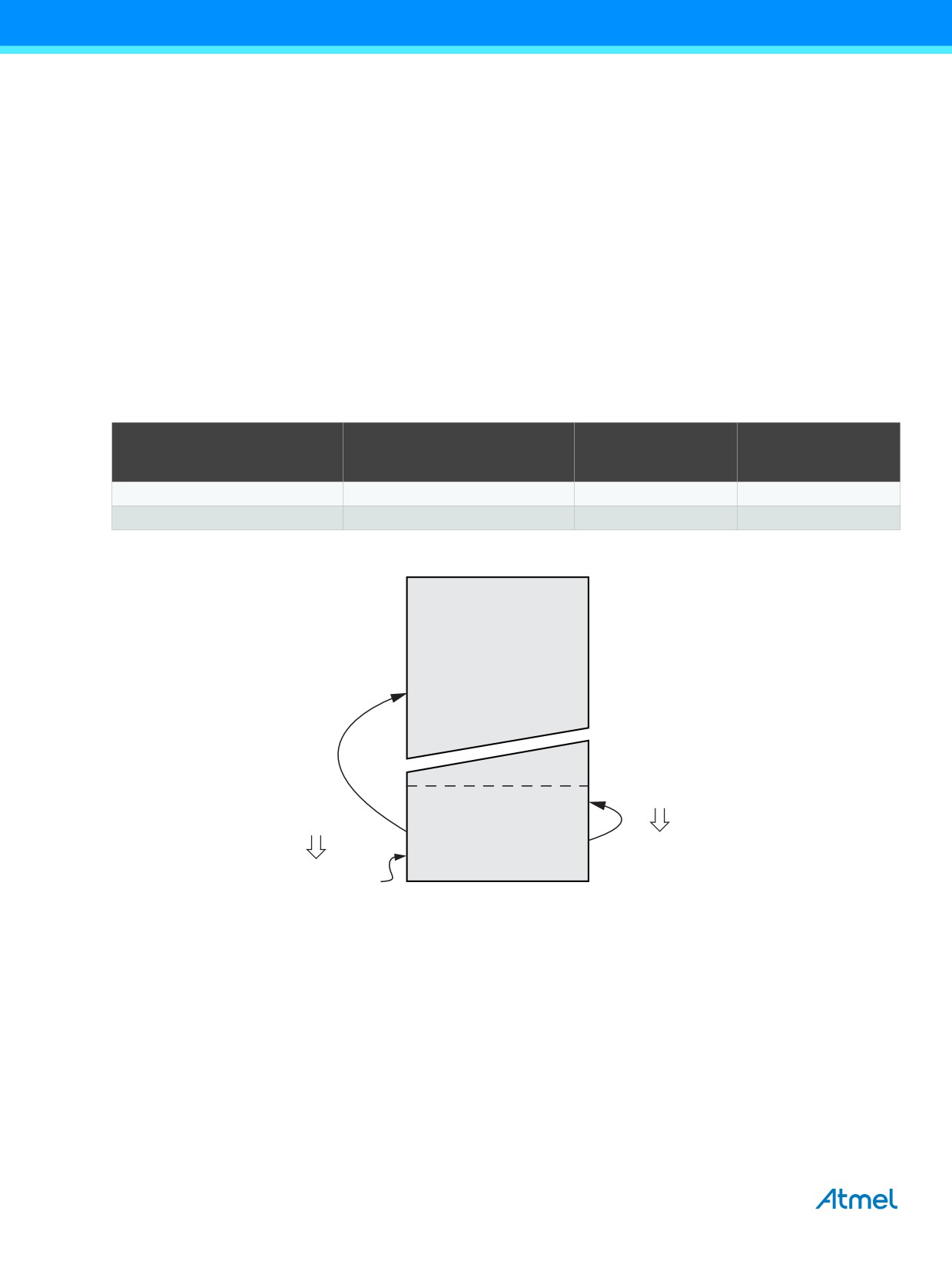
Read-While-Write and No Read-While-Write Flash Sections
Whether the CPU supports read-while-write or if the CPU is halted during a boot loader software update is dependent on
which address that is being programmed. In addition to the two sections that are configurable by the BOOTSZ fuses as
described above, the flash is also divided into two fixed sections, the read-while-write (RWW) section and the No read-while-
write (NRWW) section. The limit between the RWW- and NRWW sections is given in Figure 26-2 on page 231. The main
difference between the two sections is:
● When erasing or writing a page located inside the RWW section, the NRWW section can be read during the
operation.
● When erasing or writing a page located inside the NRWW section, the CPU is halted during the entire operation.
Note that the user software can never read any code that is located inside the RWW section during a boot loader software
operation. The syntax “read-while-write section” refers to which section that is being programmed (erased or written), not
which section that actually is being read during a boot loader software update.
ATmega328P [DATASHEET]
229
7810D-AVR-01/15
26.4.1
RWW - Read-While-Write Section
If a boot loader software update is programming a page inside the RWW section, it is possible to read code from the flash,
but only code that is located in the NRWW section. During an on-going programming, the software must ensure that the
RWW section never is being read. If the user software is trying to read code that is located inside the RWW section (i.e., by
a call/jmp/lpm or an interrupt) during programming, the software might end up in an unknown state. To avoid this, the
interrupts should either be disabled or moved to the boot loader section. The boot loader section is always located in the
NRWW section. The RWW section busy bit (RWWSB) in the store program memory control and status register (SPMCSR)
will be read as logical one as long as the RWW section is blocked for reading. After a programming is completed, the
RWWSB must be cleared by software before reading code located in the RWW section. See Section 26.9.1 “SPMCSR -
Store Program Memory Control and Status Register” on page 239 for details on how to clear RWWSB.
26.4.2
NRWW - No Read-While-Write Section
The code located in the NRWW section can be read when the boot loader software is updating a page in the RWW section.
When the boot loader code updates the NRWW section, the CPU is halted during the entire page erase or page write
operation.
Table 26-1. Read-While-Write Features
Which Section does the
Z-pointer Address during the
Which Section can be read
Read-While-Write
Programming?
during Programming?
CPU Halted?
Supported?
RWW section
NRWW section
No
Yes
NRWW section
None
Yes
No
Figure 26-1. Read-While-Write versus No Read-While-Write
Read While Write
(RWW) Section
Z-pointer
Addresses NRWW
Z-pointer
Section
Addresses RWW
Section
No Read While Write
(NRWW) Section
CPU is Halted During
the Operation
Code located in
NRWW Section
can be Read During
the Operation
230
ATmega328P [DATASHEET]
7810D-AVR-01/15
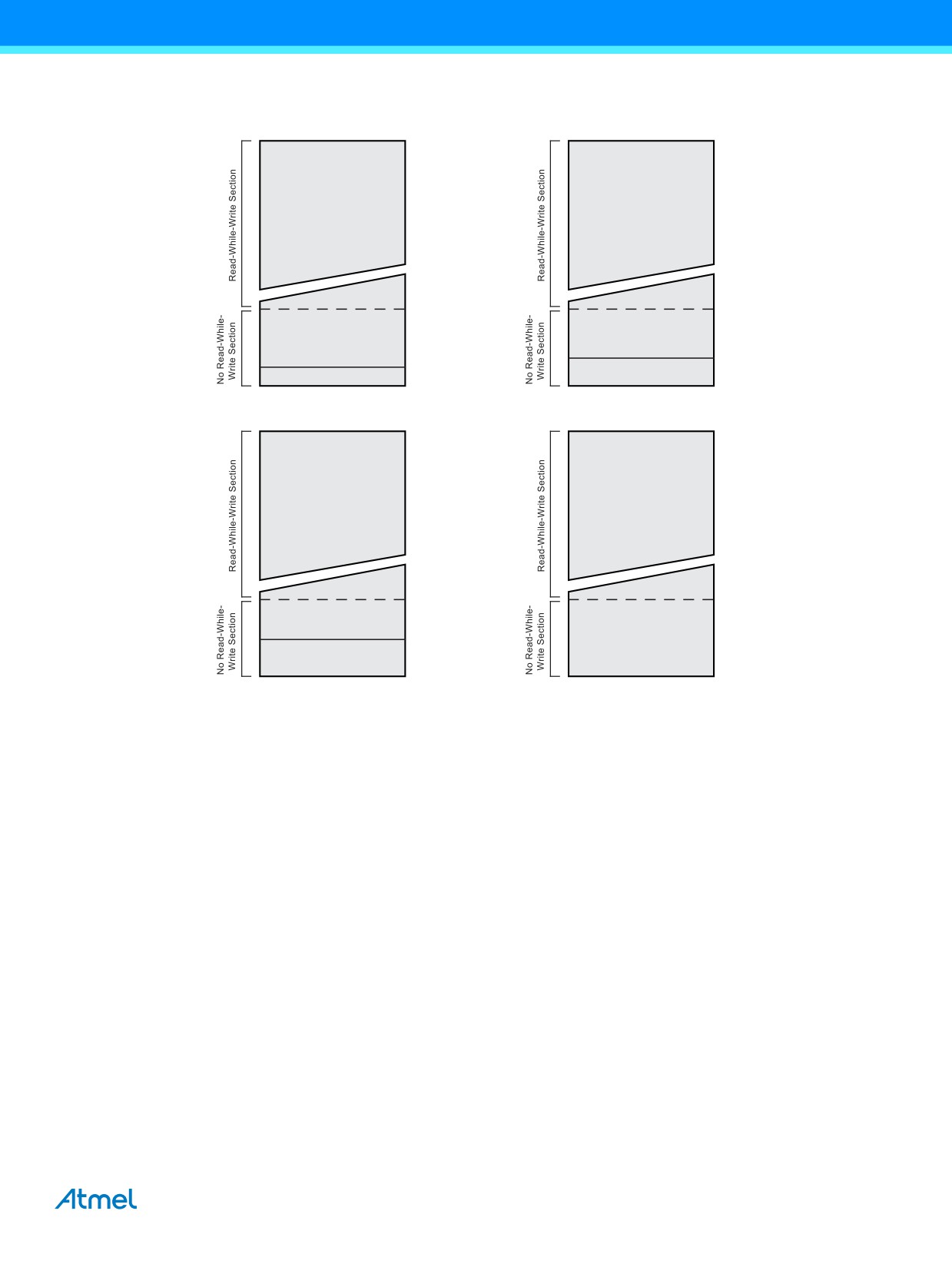
Figure 26-2. Memory Sections
Program Memory
Program Memory
BOOTSZ = ’11’
BOOTSZ = ’10’
0x0000
0x0000
Application Flash Section
Application Flash Section
End RWW
End RWW
Start NRWW
Start NRWW
Application Flash Section
Application Flash Section
End Application
End Application
Start Boot Loader
Start Boot Loader
Boot Loader Flash Section
Boot Loader Flash Section
Flashend
Flashend
Program Memory
Program Memory
BOOTSZ = ’01’
BOOTSZ = ’00’
0x0000
0x0000
Application Flash Section
Application Flash Section
End RWW, End
End RWW
Application
Start NRWW
Start NRWW,
Application Flash Section
Start Boot Loader
End Application
Boot Loader Flash Section
Start Boot Loader
Boot Loader Flash Section
Flashend
Flashend
26.5
Boot Loader Lock Bits
If no boot loader capability is needed, the entire flash is available for application code. The boot loader has two separate sets
of boot lock bits which can be set independently. This gives the user a unique flexibility to select different levels of protection.
The user can select:
● To protect the entire flash from a software update by the MCU.
● To protect only the boot loader flash section from a software update by the MCU.
● To protect only the application flash section from a software update by the MCU.
● Allow software update in the entire flash.
See Table 26-2 on page 232 and Table 26-3 on page 232 for further details. The boot lock bits can be set in software and in
serial or parallel programming mode, but they can be cleared by a chip erase command only. The general write lock (lock bit
mode 2) does not control the programming of the flash memory by SPM instruction. Similarly, the general read/write lock
(lock bit mode 1) does not control reading nor writing by LPM/SPM, if it is attempted.
ATmega328P [DATASHEET]
231
7810D-AVR-01/15

Table 26-2. Boot Lock Bit0 Protection Modes (Application Section)(1)
BLB0 Mode
BLB02
BLB01
Protection
1
1
1
No restrictions for SPM or LPM accessing the application section.
2
1
0
SPM is not allowed to write to the application section.
SPM is not allowed to write to the application section, and LPM executing
from the boot loader section is not allowed to read from the application
3
0
0
section. If interrupt vectors are placed in the boot loader section, interrupts
are disabled while executing from the application section.
LPM executing from the boot loader section is not allowed to read from the
4
0
1
application section. If interrupt vectors are placed in the boot loader section,
interrupts are disabled while executing from the application section.
Note:
1.
“1” means unprogrammed, “0” means programmed
Table 26-3. Boot Lock Bit1 Protection Modes (Boot Loader Section)(1)
BLB1 Mode
BLB12
BLB11
Protection
1
1
1
No restrictions for SPM or LPM accessing the boot loader section.
2
1
0
SPM is not allowed to write to the boot loader section.
SPM is not allowed to write to the boot loader section, and LPM executing
from the application section is not allowed to read from the boot loader
3
0
0
section. If interrupt vectors are placed in the application section, interrupts
are disabled while executing from the boot loader section.
LPM executing from the application section is not allowed to read from the
4
0
1
boot loader section. If interrupt vectors are placed in the application section,
interrupts are disabled while executing from the boot loader section.
Note:
1.
“1” means unprogrammed, “0” means programmed
26.6
Entering the Boot Loader Program
Entering the boot loader takes place by a jump or call from the application program. This may be initiated by a trigger such
as a command received via USART, or SPI interface. Alternatively, the boot reset fuse can be programmed so that the reset
vector is pointing to the boot flash start address after a reset. In this case, the boot loader is started after a reset. After the
application code is loaded, the program can start executing the application code. Note that the fuses cannot be changed by
the MCU itself. This means that once the boot reset fuse is programmed, the reset vector will always point to the boot loader
reset and the fuse can only be changed through the serial or parallel programming interface.
Table 26-4. Boot Reset Fuse(1)
BOOTRST
Reset Address
1
Reset vector = application reset (address 0x0000)
0
Reset vector = boot loader reset
Note:
1.
“1” means unprogrammed, “0” means programmed
232
ATmega328P [DATASHEET]
7810D-AVR-01/15
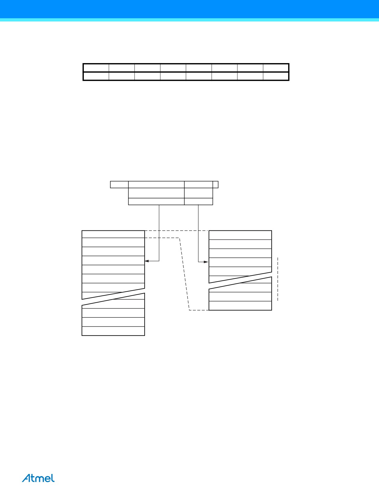
26.7
Addressing the Flash During Self-Programming
The Z-pointer is used to address the SPM commands.
Bit
15
14
13
12
11
10
9
8
ZH (R31)
Z15
Z14
Z13
Z12
Z11
Z10
Z9
Z8
ZL (R30)
Z7
Z6
Z5
Z4
Z3
Z2
Z1
Z0
7
6
5
4
3
2
1
0
Since the flash is organized in pages (see Table 27-9 on page 245), the program counter can be treated as having two
different sections. One section, consisting of the least significant bits, is addressing the words within a page, while the most
significant bits are addressing the pages. This is1 shown in Figure 26-3. Note that the page erase and page write operations
are addressed independently. Therefore it is of major importance that the boot loader software addresses the same page in
both the page erase and page write operation. Once a programming operation is initiated, the address is latched and the
Z-pointer can be used for other operations.
The only SPM operation that does not use the Z-pointer is setting the boot loader lock bits. The content of the Z-pointer is
ignored and will have no effect on the operation. The LPM instruction does also use the Z-pointer to store the address. Since
this instruction addresses the flash byte-by-byte, also the LSB (bit Z0) of the Z-pointer is used.
Figure 26-3. Addressing the Flash During SPM
Bit
15
ZPCMSB
ZPAGEMSB
1 0
Z-register
0
PCMSB
PAGEMSB
Program
PCPAGE
PCWORD
Counter
Page Address
Word Address
within the Flash
within a Page
Program Memory
Page
PCWORD[PAGEMSB:0]
Page
Instruction Word
00
01
02
PAGEEND
ATmega328P [DATASHEET]
233
7810D-AVR-01/15
26.8
Self-Programming the Flash
The program memory is updated in a page by page fashion. Before programming a page with the data stored in the
temporary page buffer, the page must be erased. The temporary page buffer is filled one word at a time using SPM and the
buffer can be filled either before the page erase command or between a page erase and a page write operation:
Alternative 1, fill the buffer before a page erase
● Fill temporary page buffer
● Perform a page erase
● Perform a page write
Alternative 2, fill the buffer after page erase
● Perform a page erase
● Fill temporary page buffer
● Perform a page write
If only a part of the page needs to be changed, the rest of the page must be stored (for example in the temporary page
buffer) before the erase, and then be rewritten. When using alternative 1, the boot loader provides an effective read-modify-
write feature which allows the user software to first read the page, do the necessary changes, and then write back the
modified data. If alternative 2 is used, it is not possible to read the old data while loading since the page is already erased.
The temporary page buffer can be accessed in a random sequence. It is essential that the page address used in both the
page erase and page write operation is addressing the same page. See Section 26.8.13 “Simple Assembly Code Example
for a Boot Loader” on page 237 for an assembly code example.
26.8.1
Performing Page Erase by SPM
To execute page erase, set up the address in the Z-pointer, write “X0000011” to SPMCSR and execute SPM within four
clock cycles after writing SPMCSR. The data in R1 and R0 is ignored. The page address must be written to PCPAGE in the
Z-register. Other bits in the Z-pointer will be ignored during this operation.
● Page erase to the RWW section: The NRWW section can be read during the page erase.
● Page erase to the NRWW section: The CPU is halted during the operation.
26.8.2
Filling the Temporary Buffer (Page Loading)
To write an instruction word, set up the address in the Z-pointer and data in R1:R0, write “00000001” to SPMCSR and
execute SPM within four clock cycles after writing SPMCSR. The content of PCWORD in the Z-register is used to address
the data in the temporary buffer. The temporary buffer will auto-erase after a page write operation or by writing the
RWWSRE bit in SPMCSR. It is also erased after a system reset. Note that it is not possible to write more than one time to
each address without erasing the temporary buffer.
If the EEPROM is written in the middle of an SPM page load operation, all data loaded will be lost.
26.8.3
Performing a Page Write
To execute page write, set up the address in the Z-pointer, write “X0000101” to SPMCSR and execute SPM within four clock
cycles after writing SPMCSR. The data in R1 and R0 is ignored. The page address must be written to PCPAGE. Other bits
in the Z-pointer must be written to zero during this operation.
● Page write to the RWW section: The NRWW section can be read during the page write.
● Page write to the NRWW section: The CPU is halted during the operation.
26.8.4
Using the SPM Interrupt
If the SPM interrupt is enabled, the SPM interrupt will generate a constant interrupt when the SELFPRGEN bit in SPMCSR is
cleared. This means that the interrupt can be used instead of polling the SPMCSR register in software. When using the SPM
interrupt, the interrupt vectors should be moved to the BLS section to avoid that an interrupt is accessing the RWW section
when it is blocked for reading. How to move the interrupts is described in Section 11. “Interrupts” on page 49.
234
ATmega328P [DATASHEET]
7810D-AVR-01/15
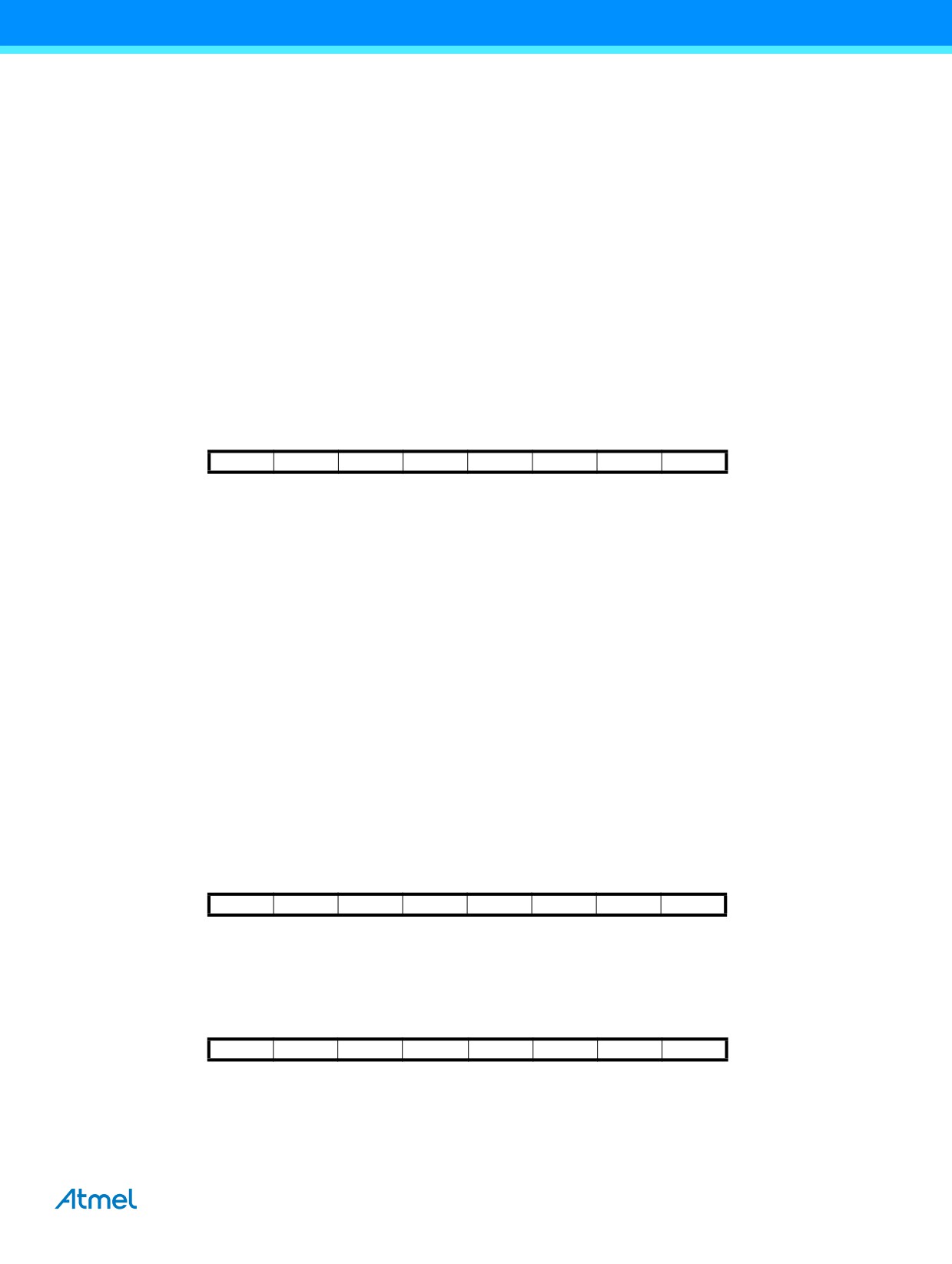
26.8.5
Consideration While Updating BLS
Special care must be taken if the user allows the boot loader section to be updated by leaving boot lock bit11
unprogrammed. An accidental write to the boot loader itself can corrupt the entire boot loader, and further software updates
might be impossible. If it is not necessary to change the boot loader software itself, it is recommended to program the boot
lock bit11 to protect the boot loader software from any internal software changes.
26.8.6
Prevent Reading the RWW Section During Self-Programming
During self-programming (either page erase or page write), the RWW section is always blocked for reading. The user
software itself must prevent that this section is addressed during the self programming operation. The RWWSB in the
SPMCSR will be set as long as the RWW section is busy. During self-programming the interrupt vector table should be
moved to the BLS as described in Section 10.8 “Watchdog Timer” on page 43, or the interrupts must be disabled. Before
addressing the RWW section after the programming is completed, the user software must clear the RWWSB by writing the
RWWSRE. See Section 26.8.13 “Simple Assembly Code Example for a Boot Loader” on page 237 for an example.
26.8.7
Setting the Boot Loader Lock Bits by SPM
To set the boot loader lock bits and general lock bits, write the desired data to R0, write “X0001001” to SPMCSR and
execute SPM within four clock cycles after writing SPMCSR.
Bit
7
6
5
4
3
2
1
0
R0
1
1
BLB12
BLB11
BLB02
BLB01
LB2
LB1
See Table 26-2 on page 232 and Table 26-3 on page 232 for how the different settings of the boot loader bits affect the flash
access.
If bits 5..0 in R0 are cleared (zero), the corresponding lock bit will be programmed if an SPM instruction is executed within
four cycles after BLBSET and SELFPRGEN are set in SPMCSR. The Z-pointer is don’t care during this operation, but for
future compatibility it is recommended to load the Z-pointer with 0x0001 (same as used for reading the lOck bits). For future
compatibility it is also recommended to set bits 7 and 6 in R0 to “1” when writing the lock bits. When programming the lock
bits the entire flash can be read during the operation.
26.8.8
EEPROM Write Prevents Writing to SPMCSR
Note that an EEPROM write operation will block all software programming to flash. Reading the fuses and lock bits from
software will also be prevented during the EEPROM write operation. It is recommended that the user checks the status bit
(EEPE) in the EECR register and verifies that the bit is cleared before writing to the SPMCSR register.
26.8.9
Reading the Fuse and Lock Bits from Software
It is possible to read both the fuse and lock bits from software. To read the lock bits, load the Z-pointer with 0x0001 and set
the BLBSET and SELFPRGEN bits in SPMCSR. When an LPM instruction is executed within three CPU cycles after the
BLBSET and SELFPRGEN bits are set in SPMCSR, the value of the lock bits will be loaded in the destination register. The
BLBSET and SELFPRGEN bits will auto-clear upon completion of reading the lock bits or if no LPM instruction is executed
within three CPU cycles or no SPM instruction is executed within four CPU cycles. When BLBSET and SELFPRGEN are
cleared, LPM will work as described in the instruction set manual.
Bit
7
6
5
4
3
2
1
0
Rd
-
-
BLB12
BLB11
BLB02
BLB01
LB2
LB1
The algorithm for reading the fuse low byte is similar to the one described above for reading the lock bits. To read the fuse
low byte, load the Z-pointer with 0x0000 and set the BLBSET and SELFPRGEN bits in SPMCSR. When an LPM instruction
is executed within three cycles after the BLBSET and SELFPRGEN bits are set in the SPMCSR, the value of the fuse low
byte (FLB) will be loaded in the destination register as shown below. Refer to Table 27-5 on page 243 for a detailed
description and mapping of the fuse low byte.
Bit
7
6
5
4
3
2
1
0
Rd
FLB7
FLB6
FLB5
FLB4
FLB3
FLB2
FLB1
FLB0
ATmega328P [DATASHEET]
235
7810D-AVR-01/15

Similarly, when reading the fuse high byte, load 0x0003 in the Z-pointer. When an LPM instruction is executed within three
cycles after the BLBSET and SELFPRGEN bits are set in the SPMCSR, the value of the fuse high byte (FHB) will be loaded
in the destination register as shown below. Refer to Table 27-7 on page 244 for detailed description and mapping of the fuse
high byte.
Bit
7
6
5
4
3
2
1
0
Rd
FHB7
FHB6
FHB5
FHB4
FHB3
FHB2
FHB1
FHB0
When reading the extended fuse byte, load 0x0002 in the Z-pointer. When an LPM instruction is executed within three cycles
after the BLBSET and SELFPRGEN bits are set in the SPMCSR, the value of the extended fuse byte (EFB) will be loaded in
the destination register as shown below. Refer to Table 27-4 on page 242 for detailed description and mapping of the
extended fuse byte.
Bit
7
6
5
4
3
2
1
0
Rd
-
-
-
-
EFB3
EFB2
EFB1
EFB0
Fuse and lock bits that are programmed, will be read as zero. Fuse and lock bits that are unprogrammed, will be read as
one.
26.8.10 Reading the Signature Row from Software
To read the signature row from software, load the Z-pointer with the signature byte address given in Table 26-5 and set the
SIGRD and SPMEN bits in SPMCSR. When an LPM instruction is executed within three CPU cycles after the SIGRD and
SPMEN bits are set in SPMCSR, the signature byte value will be loaded in the destination register. The SIGRD and SPMEN
bits will auto-clear upon completion of reading the signature row lock bits or if no LPM instruction is executed within three
CPU cycles. When SIGRD and SPMEN are cleared, LPM will work as described in the Instruction set Manual.
Table 26-5. Signature Row Addressing
Signature Byte
Z-Pointer Address
Device signature byte 1
0x0000
Device signature byte 2
0x0002
Device signature byte 3
0x0004
RC oscillator calibration byte
0x0001
TSOFFSET - temp sensor offset
0x0002
TSGAIN - temp sensor gain
0x0003
Note:
All other addresses are reserved for future use.
26.8.11 Preventing Flash Corruption
During periods of low VCC, the flash program can be corrupted because the supply voltage is too low for the CPU and the
flash to operate properly. These issues are the same as for board level systems using the flash, and the same design
solutions should be applied.
A flash program corruption can be caused by two situations when the voltage is too low. First, a regular write sequence to
the flash requires a minimum voltage to operate correctly. Secondly, the CPU itself can execute instructions incorrectly, if the
supply voltage for executing instructions is too low.
236
ATmega328P [DATASHEET]
7810D-AVR-01/15
Flash corruption can easily be avoided by following these design recommendations (one is sufficient):
1.
If there is no need for a boot loader update in the system, program the boot loader lock bits to prevent any boot
loader software updates.
2.
Keep the AVR® RESET active (low) during periods of insufficient power supply voltage. This can be done by
enabling the internal brown-out detector (BOD) if the operating voltage matches the detection level. If not, an
external low VCC reset protection circuit can be used. If a reset occurs while a write operation is in progress, the
write operation will be completed provided that the power supply voltage is sufficient.
3.
Keep the AVR core in power-down sleep mode during periods of low VCC. This will prevent the CPU from
attempting to decode and execute instructions, effectively protecting the SPMCSR register and thus the flash from
unintentional writes.
26.8.12 Programming Time for Flash when Using SPM
The calibrated RC oscillator is used to time flash accesses. Table 26-6 shows the typical programming time for flash
accesses from the CPU.
Table 26-6. SPM Programming Time(1)
Symbol
Min Programming Time
Max Programming Time
Flash write (page erase, page write, and write lock
3.7ms
4.5ms
bits by SPM)
Note:
1.
Minimum and maximum programming time is per individual operation.
26.8.13
Simple Assembly Code Example for a Boot Loader
;-the routine writes one page of data from RAM to Flash
; the first data location in RAM is pointed to by the Y pointer
; the first data location in Flash is pointed to by the Z-pointer
;-error handling is not included
;-the routine must be placed inside the Boot space
; (at least the Do_spm sub routine). Only code inside NRWW section can
; be read during Self-Programming (Page Erase and Page Write).
;-registers used: r0, r1, temp1 (r16), temp2 (r17), looplo (r24),
; loophi (r25), spmcrval (r20)
; storing and restoring of registers is not included in the routine
; register usage can be optimized at the expense of code size
;-It is assumed that either the interrupt table is moved to the Boot
; loader section or that the interrupts are disabled.
.equ
PAGESIZEB = PAGESIZE*2
;PAGESIZEB is page size in BYTES, not words
.org SMALLBOOTSTART
Write_page:
;Page Erase
ldi
spmcrval, (1<<PGERS) | (1<<SELFPRGEN)
call
Do_spm
;re-enable the RWW section
ldi
spmcrval, (1<<RWWSRE) | (1<<SELFPRGEN)
call
Do_spm
;transfer data from RAM to Flash page buffer
ldi
looplo, low(PAGESIZEB)
;init loop variable
ldi
loophi, high(PAGESIZEB)
;not required for PAGESIZEB<=256
Wrloop:
ld
r0, Y+
ld
r1, Y+
ldi
spmcrval, (1<<SELFPRGEN)
call
Do_spm
adiw
ZH:ZL, 2
ATmega328P [DATASHEET]
237
7810D-AVR-01/15
sbiw
loophi:looplo, 2
;use subi for PAGESIZEB<=256
brne
Wrloop
;execute Page Write
subi
ZL, low(PAGESIZEB)
;restore pointer
sbci
ZH, high(PAGESIZEB)
;not required for PAGESIZEB<=256
ldi
spmcrval, (1<<PGWRT) | (1<<SELFPRGEN)
call
Do_spm
;re-enable the RWW section
ldi
spmcrval, (1<<RWWSRE) | (1<<SELFPRGEN)
call
Do_spm
;read back and check, optional
ldi
looplo, low(PAGESIZEB)
;init loop variable
ldi
loophi, high(PAGESIZEB)
;not required for PAGESIZEB<=256
subi
YL, low(PAGESIZEB)
;restore pointer
sbci
YH, high(PAGESIZEB)
Rdloop:
lpm
r0, Z+
ld
r1, Y+
cpse
r0, r1
jmp
Error
sbiw
loophi:looplo, 1
;use subi for PAGESIZEB<=256
brne
Rdloop
;return to RWW section
;verify that RWW section is safe to read
Return:
in
temp1, SPMCSR
sbrs
temp1, RWWSB
; If RWWSB is set, the RWW section is not ready yet
ret
;re-enable the RWW section
ldi
spmcrval, (1<<RWWSRE) | (1<<SELFPRGEN)
call
Do_spm
rjmp
Return
Do_spm:
;check for previous SPM complete
Wait_spm:
in
temp1, SPMCSR
sbrc
temp1, SELFPRGEN
rjmp
Wait_spm
;input: spmcrval determines SPM action
;disable interrupts if enabled, store status
in
temp2, SREG
cli
;check that no EEPROM write access is present
Wait_ee:
sbic
EECR, EEPE
rjmp
Wait_ee
;SPM timed sequence
out
SPMCSR, spmcrval
spm
;restore SREG (to enable interrupts if originally enabled)
out
SREG, temp2
ret
238
ATmega328P [DATASHEET]
7810D-AVR-01/15

26.8.14 ATmega328P Boot Loader Parameters
In Table 26-7 through Table 26-9, the parameters used in the description of the self programming are given.
Table 26-7. Boot Size Configuration, ATmega328P
Application
Boot Loader
End Application
Boot Reset Address (Start
BOOTSZ1
BOOTSZ0
Boot Size
Pages
Flash Section
Flash Section
Section
Boot Loader Section)
1
1
256 words
4
0x0000 - 0x3EFF
0x3F00 - 0x3FFF
0x3EFF
0x3F00
1
0
512 words
8
0x0000 - 0x3DFF
0x3E00 - 0x3FFF
0x3DFF
0x3E00
0
1
1024 words
16
0x0000 - 0x3BFF
0x3C00 - 0x3FFF
0x3BFF
0x3C00
0
0
2048 words
32
0x0000 - 0x37FF
0x3800 - 0x3FFF
0x37FF
0x3800
Note:
The different BOOTSZ fuse configurations are shown in Figure 26-2 on page 231.
Table 26-8. Read-While-Write Limit, ATmega328P
Section
Pages
Address
Read-while-write section (RWW)
224
0x0000 - 0x37FF
No read-while-write section (NRWW)
32
0x3800 - 0x3FFF
For details about these two section, see Section 26.4.2 “NRWW - No Read-While-Write Section” on page 230 and Section
26.4.1 “RWW - Read-While-Write Section” on page 230.
Table 26-9. Explanation of Different Variables used in Figure 26-3 and the Mapping to the Z-pointer, ATmega328P
Corresponding
Variable
Z-value(1)
Description
Most significant bit in the program counter. (the program
PCMSB
13
counter is 14 bits PC[13:0])
Most significant bit which is used to address the words within
PAGEMSB
5
one page (64 words in a page requires 6 bits PC [5:0])
Bit in Z-register that is mapped to PCMSB. Because Z0 is not
ZPCMSB
Z14
used, the ZPCMSB equals PCMSB + 1.
Bit in Z-register that is mapped to PAGEMSB. Because Z0 is
ZPAGEMSB
Z6
not used, the ZPAGEMSB equals PAGEMSB + 1.
Program counter page address: Page select, for page erase
PCPAGE
PC[13:6]
Z14:Z7
and page write
Program counter word address: Word select, for filling
PCWORD
PC[5:0]
Z6:Z1
temporary buffer (must be zero during page write operation)
Note:
1.
Z15: always ignored
Z0: should be zero for all SPM commands, byte select for the LPM instruction.
See Section 26.7 “Addressing the Flash During Self-Programming” on page 233 for details about the use of
Z-pointer during self-programming.
26.9
Register Description
26.9.1
SPMCSR - Store Program Memory Control and Status Register
The store program memory control and status register contains the control bits needed to control the boot loader operations.
Bit
7
6
5
4
3
2
1
0
0x37 (0x57)
SPMIE
RWWSB
-
RWWSRE
BLBSET
PGWRT
PGERS
SELFPRGEN
SPMCSR
Read/Write
R/W
R
R
R/W
R/W
R/W
R/W
R/W
Initial Value
0
0
0
0
0
0
0
0
ATmega328P [DATASHEET]
239
7810D-AVR-01/15