Atmel ATmega328P 8-bit AVR Microcontroller. DATASHEET (2015) - page 4
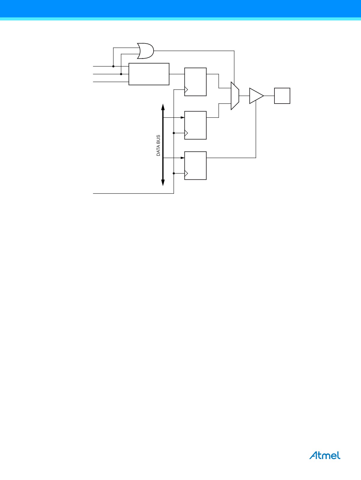
Figure 17-4. Compare Match Output Unit, Schematic
COMnx1
COMnx0
Waveform
D
Q
Generator
FOCnx
1
OCnx
OCnx
Pin
0
D
Q
PORT
D
Q
DDR
clkI/O
The general I/O port function is overridden by the output compare (OC2x) from the waveform generator if either of the
COM2x1:0 bits are set. However, the OC2x pin direction (input or output) is still controlled by the data direction register
(DDR) for the port pin. The data direction register bit for the OC2x pin (DDR_OC2x) must be set as output before the OC2x
value is visible on the pin. The port override function is independent of the waveform generation mode.
The design of the output compare pin logic allows initialization of the OC2x state before the output is enabled. Note that
some COM2x1:0 bit settings are reserved for certain modes of operation. See Section 17.11 “Register Description” on page
127.
17.6.1
Compare Output Mode and Waveform Generation
The waveform generator uses the COM2x1:0 bits differently in normal, CTC, and PWM modes. For all modes, setting the
COM2x1:0 = 0 tells the waveform generator that no action on the OC2x register is to be performed on the next compare
match. For compare output actions in the non-PWM modes refer to Table 17-5 on page 129. For fast PWM mode, refer to
Table 17-6 on page 129, and for phase correct PWM refer to Table 17-7 on page 129.
A change of the COM2x1:0 bits state will have effect at the first compare match after the bits are written. For non-PWM
modes, the action can be forced to have immediate effect by using the FOC2x strobe bits.
17.7
Modes of Operation
The mode of operation, i.e., the behavior of the Timer/Counter and the output compare pins, is defined by the combination of
the waveform generation mode (WGM22:0) and compare output mode (COM2x1:0) bits. The compare output mode bits do
not affect the counting sequence, while the waveform generation mode bits do. The COM2x1:0 bits control whether the
PWM output generated should be inverted or not (inverted or non-inverted PWM). For non-PWM modes the COM2x1:0 bits
control whether the output should be set, cleared, or toggled at a compare match (see Section 17.6 “Compare Match Output
Unit” on page 119).
For detailed timing information refer to Section 17.8 “Timer/Counter Timing Diagrams” on page 124.
120
ATmega328P [DATASHEET]
7810D-AVR-01/15
17.7.1
Normal Mode
The simplest mode of operation is the normal mode (WGM22:0 = 0). In this mode the counting direction is always up
(incrementing), and no counter clear is performed. The counter simply overruns when it passes its maximum 8-bit value
(TOP = 0xFF) and then restarts from the bottom (0x00). In normal operation the Timer/Counter overflow flag (TOV2) will be
set in the same timer clock cycle as the TCNT2 becomes zero. The TOV2 flag in this case behaves like a ninth bit, except
that it is only set, not cleared. However, combined with the timer overflow interrupt that automatically clears the TOV2 flag,
the timer resolution can be increased by software. There are no special cases to consider in the normal mode, a new counter
value can be written anytime.
The output compare unit can be used to generate interrupts at some given time. Using the output compare to generate
waveforms in normal mode is not recommended, since this will occupy too much of the CPU time.
17.7.2
Clear Timer on Compare Match (CTC) Mode
In clear timer on compare or CTC mode (WGM22:0 = 2), the OCR2A register is used to manipulate the counter resolution. In
CTC mode the counter is cleared to zero when the counter value (TCNT2) matches the OCR2A. The OCR2A defines the top
value for the counter, hence also its resolution. This mode allows greater control of the compare match output frequency. It
also simplifies the operation of counting external events.
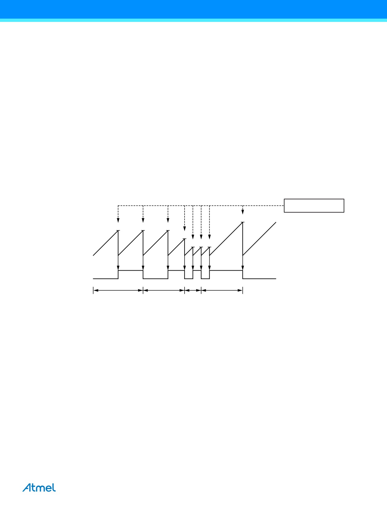
The timing diagram for the CTC mode is shown in Figure 17-5. The counter value (TCNT2) increases until a compare match
occurs between TCNT2 and OCR2A, and then counter (TCNT2) is cleared.
Figure 17-5. CTC Mode, Timing Diagram
OCnx Interrupt Flag Set
TCNTn
OCnx
(COMnA1:0 = 1)
(Toggle)
1
2
3
4
Period
An interrupt can be generated each time the counter value reaches the TOP value by using the OCF2A flag. If the interrupt
is enabled, the interrupt handler routine can be used for updating the TOP value. However, changing TOP to a value close to
BOTTOM when the counter is running with none or a low prescaler value must be done with care since the CTC mode does
not have the double buffering feature. If the new value written to OCR2A is lower than the current value of TCNT2, the
counter will miss the compare match. The counter will then have to count to its maximum value (0xFF) and wrap around
starting at 0x00 before the compare match can occur.
For generating a waveform output in CTC mode, the OC2A output can be set to toggle its logical level on each compare
match by setting the compare output mode bits to toggle mode (COM2A1:0 = 1). The OC2A value will not be visible on the
port pin unless the data direction for the pin is set to output. The waveform generated will have a maximum frequency of
fOC2A = fclk_I/O/2 when OCR2A is set to zero (0x00). The waveform frequency is defined by the following equation:
fclk_I/O
fOCnx
= ----------------------------------------------------
2 N 1 + OCRnx
The N variable represents the prescale factor (1, 8, 32, 64, 128, 256, or 1024).
As for the normal mode of operation, the TOV2 flag is set in the same timer clock cycle that the counter counts from MAX to
0x00.
ATmega328P [DATASHEET]
121
7810D-AVR-01/15
17.7.3
Fast PWM Mode
The fast pulse width modulation or fast PWM mode (WGM22:0 = 3 or 7) provides a high frequency PWM waveform
generation option. The fast PWM differs from the other PWM option by its single-slope operation. The counter counts from
BOTTOM to TOP then restarts from BOTTOM. TOP is defined as 0xFF when WGM2:0 = 3, and OCR2A when MGM2:0 = 7.
In non-inverting compare output mode, the output compare (OC2x) is cleared on the compare match between TCNT2 and
OCR2x, and set at BOTTOM. In inverting compare output mode, the output is set on compare match and cleared at
BOTTOM. Due to the single-slope operation, the operating frequency of the fast PWM mode can be twice as high as the
phase correct PWM mode that uses dual-slope operation. This high frequency makes the fast PWM mode well suited for
power regulation, rectification, and DAC applications. High frequency allows physically small sized external components
(coils, capacitors), and therefore reduces total system cost.
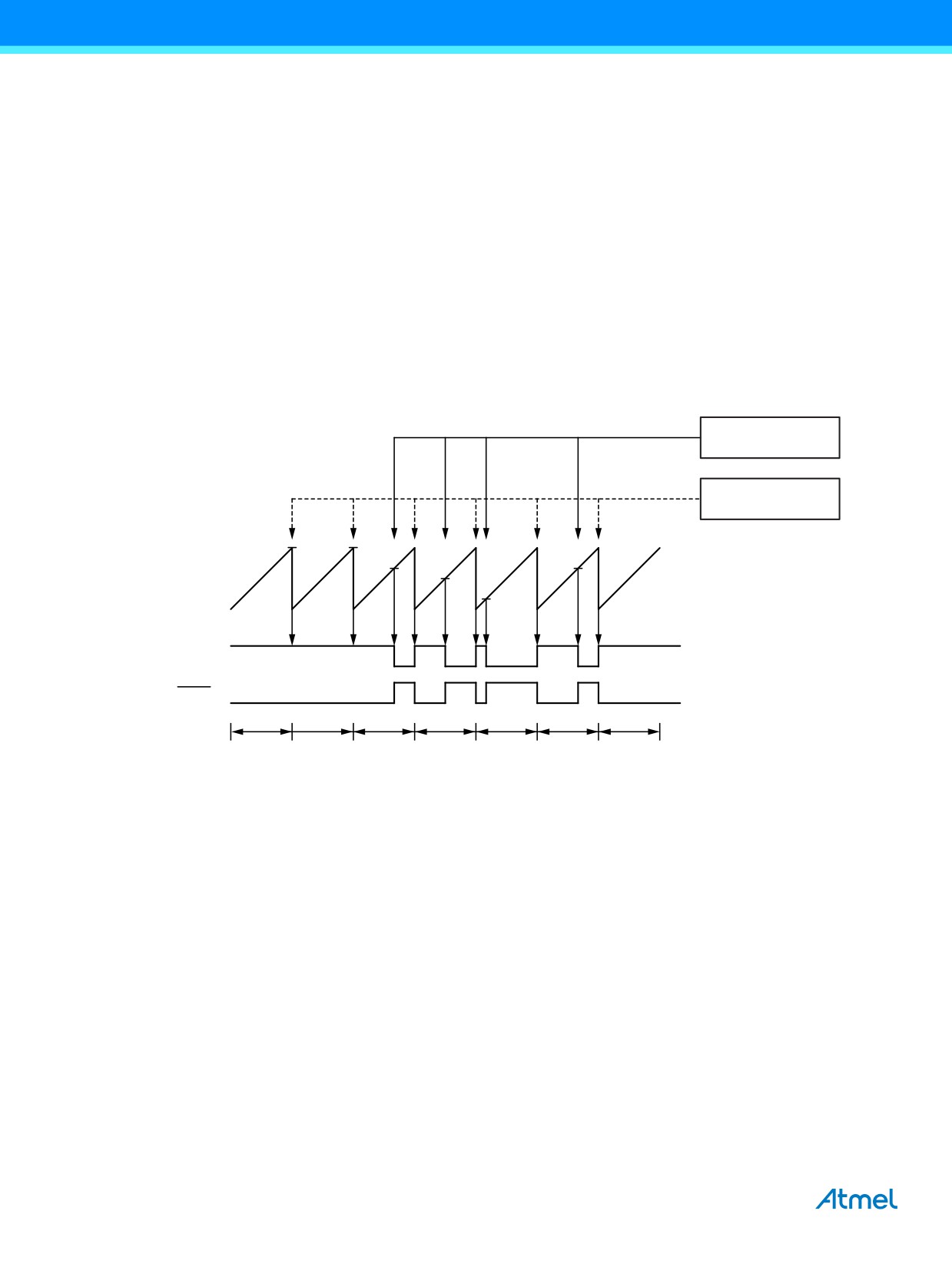
In fast PWM mode, the counter is incremented until the counter value matches the TOP value. The counter is then cleared at
the following timer clock cycle. The timing diagram for the fast PWM mode is shown in Figure 17-6. The TCNT2 value is in
the timing diagram shown as a histogram for illustrating the single-slope operation. The diagram includes non-inverted and
inverted PWM outputs. The small horizontal line marks on the TCNT2 slopes represent compare matches between OCR2x
and TCNT2.
Figure 17-6. Fast PWM Mode, Timing Diagram
OCRnx Interrupt
Flag Set
OCRnx Update and
TOVn Interrupt Flag Set
TCNTn
OCnx
(COMnx1:0 = 2)
OCnx
(COMnx1:0 = 3)
1
2
3
4
5
6
7
Period
The Timer/Counter overflow flag (TOV2) is set each time the counter reaches TOP. If the interrupt is enabled, the interrupt
handler routine can be used for updating the compare value.
In fast PWM mode, the compare unit allows generation of PWM waveforms on the OC2x pin. Setting the COM2x1:0 bits to
two will produce a non-inverted PWM and an inverted PWM output can be generated by setting the COM2x1:0 to three. TOP
is defined as 0xFF when WGM2:0 = 3, and OCR2A when MGM2:0 = 7. (See Table 17-3 on page 128). The actual OC2x
value will only be visible on the port pin if the data direction for the port pin is set as output. The PWM waveform is generated
by setting (or clearing) the OC2x register at the compare match between OCR2x and TCNT2, and clearing (or setting) the
OC2x register at the timer clock cycle the counter is cleared (changes from TOP to BOTTOM).
The PWM frequency for the output can be calculated by the following equation:
fclk_I/O
fOCnxPWM
= -------------------
N 256
The N variable represents the prescale factor (1, 8, 32, 64, 128, 256, or 1024).
The extreme values for the OCR2A register represent special cases when generating a PWM waveform output in the fast
PWM mode. If the OCR2A is set equal to BOTTOM, the output will be a narrow spike for each MAX+1 timer clock cycle.
Setting the OCR2A equal to MAX will result in a constantly high or low output (depending on the polarity of the output set by
the COM2A1:0 bits.)
122
ATmega328P [DATASHEET]
7810D-AVR-01/15
A frequency (with 50% duty cycle) waveform output in fast PWM mode can be achieved by setting OC2x to toggle its logical
level on each compare match (COM2x1:0 = 1). The waveform generated will have a maximum frequency of foc2 = fclk_I/O/2
when OCR2A is set to zero. This feature is similar to the OC2A toggle in CTC mode, except the double buffer feature of the
output compare unit is enabled in the fast PWM mode.
17.7.4
Phase Correct PWM Mode
The phase correct PWM mode (WGM22:0 = 1 or 5) provides a high resolution phase correct PWM waveform generation
option. The phase correct PWM mode is based on a dual-slope operation. The counter counts repeatedly from BOTTOM to
TOP and then from TOP to BOTTOM. TOP is defined as 0xFF when WGM2:0 = 3, and OCR2A when MGM2:0 = 7.
In non-inverting compare output mode, the output compare (OC2x) is cleared on the compare match between TCNT2 and
OCR2x while upcounting, and set on the compare match while downcounting. In inverting output compare mode, the
operation is inverted. The dual-slope operation has lower maximum operation frequency than single slope operation.
However, due to the symmetric feature of the dual-slope PWM modes, these modes are preferred for motor control
applications.
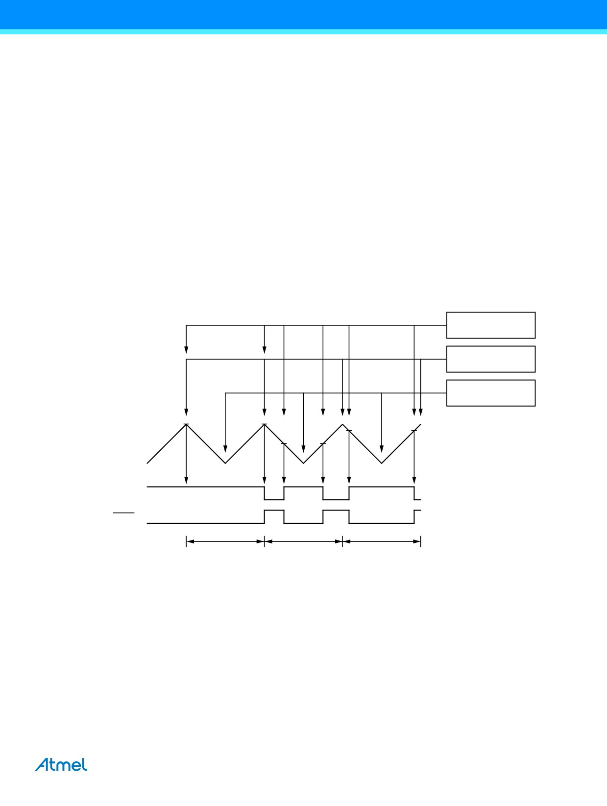
In phase correct PWM mode the counter is incremented until the counter value matches TOP. When the counter reaches
TOP, it changes the count direction. The TCNT2 value will be equal to TOP for one timer clock cycle. The timing diagram for
the phase correct PWM mode is shown on Figure 17-7. The TCNT2 value is in the timing diagram shown as a histogram for
illustrating the dual-slope operation. The diagram includes non-inverted and inverted PWM outputs. The small horizontal line
marks on the TCNT2 slopes represent compare matches between OCR2x and TCNT2.
Figure 17-7. Phase Correct PWM Mode, Timing Diagram
OCnx Interrupt
Flag Set
OCRnx Update
TOVn Interrupt
Flag Set
TCNTn
(COMnx1:0 = 2)
OCnx
OCnx
(COMnx1:0 = 3)
1
2
3
Period
The Timer/Counter overflow flag (TOV2) is set each time the counter reaches BOTTOM. The interrupt flag can be used to
generate an interrupt each time the counter reaches the BOTTOM value.
ATmega328P [DATASHEET]
123
7810D-AVR-01/15
In phase correct PWM mode, the compare unit allows generation of PWM waveforms on the OC2x pin. Setting the
COM2x1:0 bits to two will produce a non-inverted PWM. An inverted PWM output can be generated by setting the
COM2x1:0 to three. TOP is defined as 0xFF when WGM2:0 = 3, and OCR2A when MGM2:0 = 7 (See Table 17-4 on page
128). The actual OC2x value will only be visible on the port pin if the data direction for the port pin is set as output. The PWM
waveform is generated by clearing (or setting) the OC2x register at the compare match between OCR2x and TCNT2 when
the counter increments, and setting (or clearing) the OC2x register at compare match between OCR2x and TCNT2 when the
counter decrements. The PWM frequency for the output when using phase correct PWM can be calculated by the following
equation:
fclk_I/O
fOCnxPCPWM
= -------------------
N 510
The N variable represents the prescale factor (1, 8, 32, 64, 128, 256, or 1024).
The extreme values for the OCR2A register represent special cases when generating a PWM waveform output in the phase
correct PWM mode. If the OCR2A is set equal to BOTTOM, the output will be continuously low and if set equal to MAX the
output will be continuously high for non-inverted PWM mode. For inverted PWM the output will have the opposite logic
values.
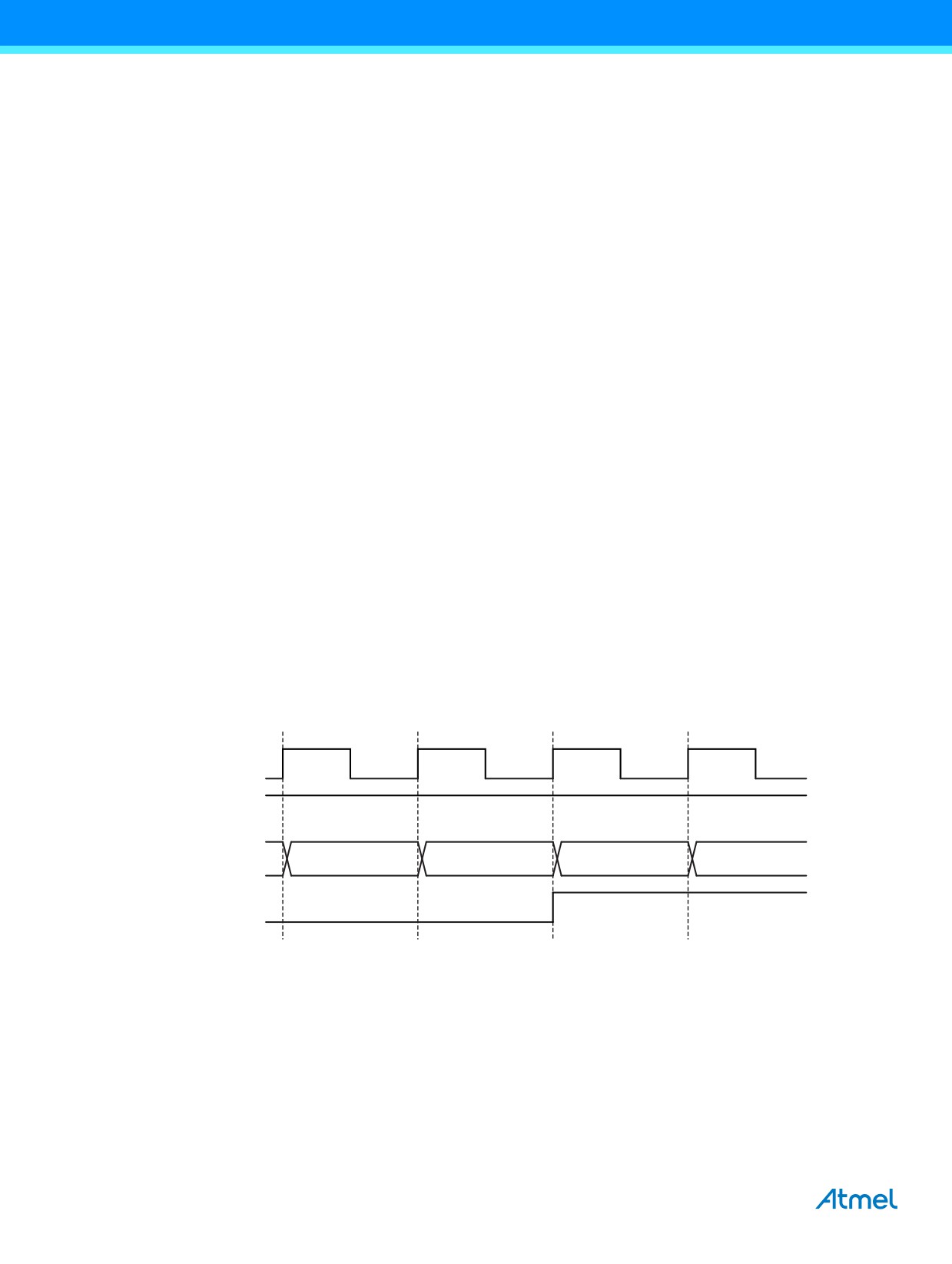
At the very start of period 2 in Figure 17-7 on page 123 OCnx has a transition from high to low even though there is no
compare match. The point of this transition is to guarantee symmetry around BOTTOM. There are two cases that give a
transition without compare match.
● OCR2A changes its value from MAX, like in Figure 17-7 on page 123. When the OCR2A value is MAX the OCn pin
value is the same as the result of a down-counting compare match. To ensure symmetry around BOTTOM the OCn
value at MAX must correspond to the result of an up-counting compare match.
● The timer starts counting from a value higher than the one in OCR2A, and for that reason misses the compare match
and hence the OCn change that would have happened on the way up.
17.8
Timer/Counter Timing Diagrams
The following figures show the Timer/Counter in synchronous mode, and the timer clock (clkT2) is therefore shown as a clock
enable signal. In asynchronous mode, clkI/O should be replaced by the Timer/Counter oscillator clock. The figures include
information on when interrupt flags are set. Figure 17-8 contains timing data for basic Timer/Counter operation. The figure
shows the count sequence close to the MAX value in all modes other than phase correct PWM mode.
Figure 17-8. Timer/Counter Timing Diagram, no Prescaling
clkI/O
clkTn
(clkI/O/1)
TCNTn
MAX - 1
MAX
BOTTOM
BOTTOM + 1
TOVn
124
ATmega328P [DATASHEET]
7810D-AVR-01/15
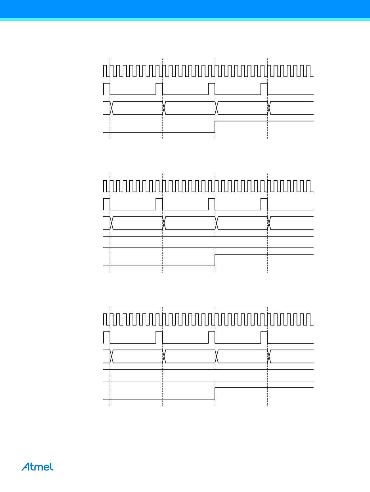
Figure 17-9 shows the same timing data, but with the prescaler enabled.
Figure 17-9. Timer/Counter Timing Diagram, with Prescaler (fclk_I/O/8)
clkI/O
clkTn
(clkI/O/8)
TCNTn
MAX - 1
MAX
BOTTOM
BOTTOM + 1
TOVn
Figure 17-10 shows the setting of OCF2A in all modes except CTC mode.
Figure 17-10. Timer/Counter Timing Diagram, Setting of OCF2A, with Prescaler (fclk_I/O/8)
clkI/O
clkTn
(clkI/O/8)
TCNTn
OCRnx - 1
OCRnx
OCRnx + 1
OCRnx + 2
OCRnx
OCRnx Value
OCFnx
Figure 17-11 shows the setting of OCF2A and the clearing of TCNT2 in CTC mode.
Figure 17-11. Timer/Counter Timing Diagram, Clear Timer on Compare Match Mode, with Prescaler (fclk_I/O/8)
clkI/O
clkTn
(clkI/O/8)
TCNTn
TOP - 1
TOP
BOTTOM
BOTTOM + 1
(CTC)
OCRnx
TOP
OCFnx
ATmega328P [DATASHEET]
125
7810D-AVR-01/15
17.9
Asynchronous Operation of Timer/Counter2
When Timer/Counter2 operates asynchronously, some considerations must be taken.
●
Warning: When switching between asynchronous and synchronous clocking of Timer/Counter2, the Timer Registers
TCNT2, OCR2x, and TCCR2x might be corrupted. A safe procedure for switching clock source is:
a.
Disable the Timer/Counter2 interrupts by clearing OCIE2x and TOIE2.
b.
Select clock source by setting AS2 as appropriate.
c.
Write new values to TCNT2, OCR2x, and TCCR2x.
d.
To switch to asynchronous operation: Wait for TCN2xUB, OCR2xUB, and TCR2xUB.
e.
Clear the Timer/Counter2 interrupt flags.
f.
Enable interrupts, if needed.
●
The CPU main clock frequency must be more than four times the oscillator frequency.
●
When writing to one of the registers TCNT2, OCR2x, or TCCR2x, the value is transferred to a temporary register, and
latched after two positive edges on TOSC1. The user should not write a new value before the contents of the
temporary register have been transferred to its destination. Each of the five mentioned registers have their individual
temporary register, which means that e.g. writing to TCNT2 does not disturb an OCR2x write in progress. To detect
that a transfer to the destination register has taken place, the asynchronous status register - ASSR has been
implemented.
●
When entering power-save or ADC noise reduction mode after having written to TCNT2, OCR2x, or TCCR2x, the
user must wait until the written register has been updated if Timer/Counter2 is used to wake up the device. Otherwise,
the MCU will enter sleep mode before the changes are effective. This is particularly important if any of the output
compare2 interrupt is used to wake up the device, since the output compare function is disabled during writing to
OCR2x or TCNT2. If the write cycle is not finished, and the MCU enters sleep mode before the corresponding
OCR2xUB bit returns to zero, the device will never receive a compare match interrupt, and the MCU will not wake up.
●
If Timer/Counter2 is used to wake the device up from power-save or ADC noise reduction mode, precautions must be
taken if the user wants to re-enter one of these modes: If re-entering sleep mode within the TOSC1 cycle, the interrupt
will immediately occur and the device wake up again. The result is multiple interrupts and wake-ups within one
TOSC1 cycle from the first interrupt. If the user is in doubt whether the time before re-entering power-save or ADC
noise reduction mode is sufficient, the following algorithm can be used to ensure that one TOSC1 cycle has elapsed:
a. Write a value to TCCR2x, TCNT2, or OCR2x.
b. Wait until the corresponding update busy flag in ASSR returns to zero.
c. Enter power-save or ADC noise reduction mode.
●
When the asynchronous operation is selected, the 32.768kHz oscillator for Timer/Counter2 is always running, except
in power-down and standby modes. After a power-up reset or wake-up from power-down or standby mode, the user
should be aware of the fact that this oscillator might take as long as one second to stabilize. The user is advised to
wait for at least one second before using Timer/Counter2 after power-up or wake-up from power-down or standby
mode. The contents of all Timer/Counter2 registers must be considered lost after a wake-up from power-down or
standby mode due to unstable clock signal upon start-up, no matter whether the oscillator is in use or a clock signal is
applied to the TOSC1 pin.
●
Description of wake up from power-save or ADC noise reduction mode when the timer is clocked asynchronously:
When the interrupt condition is met, the wake up process is started on the following cycle of the timer clock, that is,
the timer is always advanced by at least one before the processor can read the counter value. After wake-up, the
MCU is halted for four cycles, it executes the interrupt routine, and resumes execution from the instruction following
SLEEP.
●
Reading of the TCNT2 register shortly after wake-up from power-save may give an incorrect result. Since TCNT2 is
clocked on the asynchronous TOSC clock, reading TCNT2 must be done through a register synchronized to the
internal I/O clock domain. Synchronization takes place for every rising TOSC1 edge. When waking up from
power-save mode, and the I/O clock (clkI/O) again becomes active, TCNT2 will read as the previous value (before
entering sleep) until the next rising TOSC1 edge. The phase of the TOSC clock after waking up from power-save
mode is essentially unpredictable, as it depends on the wake-up time. The recommended procedure for reading
TCNT2 is thus as follows:
126
ATmega328P [DATASHEET]
7810D-AVR-01/15
a. Write any value to either of the registers OCR2x or TCCR2x.
b. Wait for the corresponding update busy flag to be cleared.
c. Read TCNT2.
During asynchronous operation, the synchronization of the interrupt flags for the asynchronous timer takes 3 processor
cycles plus one timer cycle. The timer is therefore advanced by at least one before the processor can read the timer value
causing the setting of the interrupt flag. The output compare pin is changed on the timer clock and is not synchronized to the
processor clock.
17.10
Timer/Counter Prescaler
Figure 17-12.Prescaler for Timer/Counter2
clkI/O
T2S
clk
10-bit T/C Prescaler
Clear
TOSC1
AS2
PSRASY
0
CS20
CS21
CS22
Timer/Counter2 Clock Source
clkT2
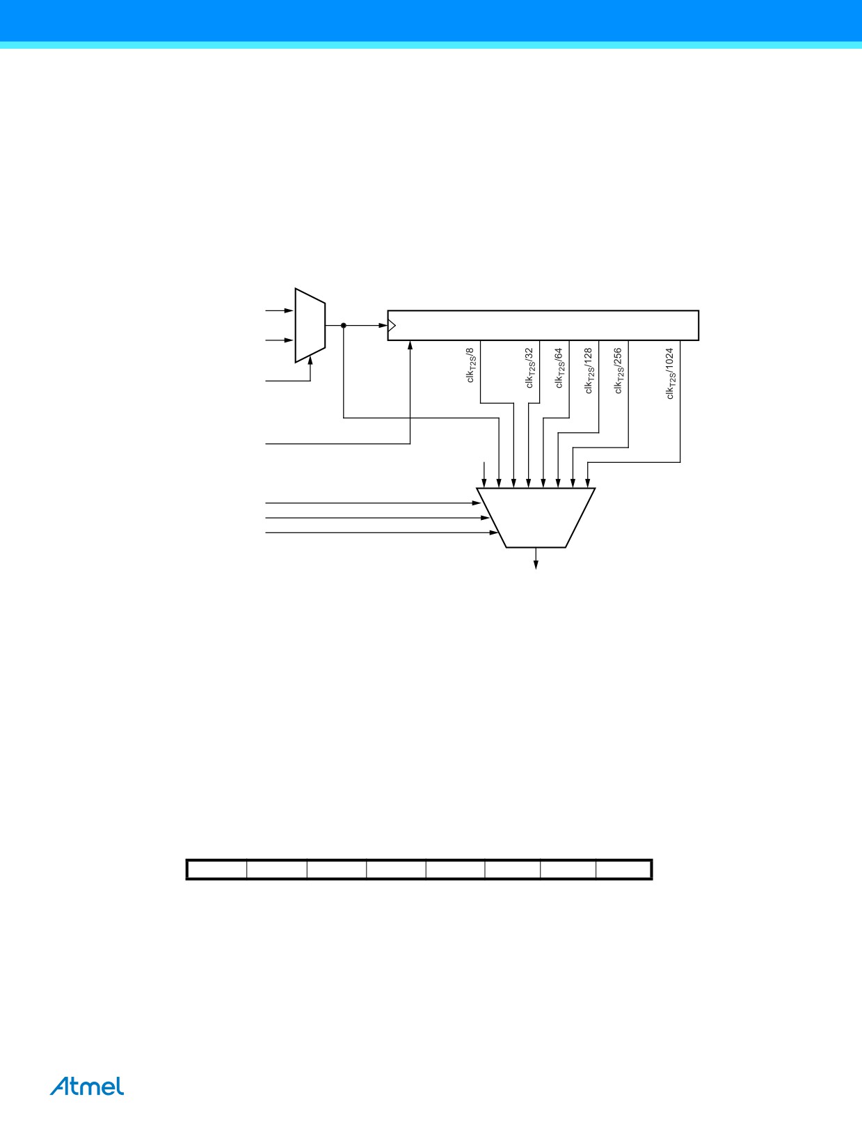
The clock source for Timer/Counter2 is named clkT2S. clkT2S is by default connected to the main system I/O clock clkIO. By
setting the AS2 bit in ASSR, Timer/Counter2 is asynchronously clocked from the TOSC1 pin. This enables use of
Timer/Counter2 as a real time counter (RTC). When AS2 is set, pins TOSC1 and TOSC2 are disconnected from port C. A
crystal can then be connected between the TOSC1 and TOSC2 pins to serve as an independent clock source for
Timer/Counter2. The oscillator is optimized for use with a 32.768kHz crystal.
For Timer/Counter2, the possible prescaled selections are: clkT2S/8, clkT2S/32, clkT2S/64, clkT2S/128, clkT2S/256, and
clkT2S/1024. Additionally, clkT2S as well as 0 (stop) may be selected. Setting the PSRASY bit in GTCCR resets the prescaler.
This allows the user to operate with a predictable prescaler.
17.11
Register Description
17.11.1 TCCR2A - Timer/Counter Control Register A
Bit
7
6
5
4
3
2
1
0
(0xB0)
COM2A1
COM2A0
COM2B1
COM2B0
-
-
WGM21
WGM20
TCCR2A
Read/Write
R/W
R/W
R/W
R/W
R
R
R/W
R/W
Initial Value
0
0
0
0
0
0
0
0
• Bits 7:6 - COM2A1:0: Compare Match Output A Mode
These bits control the output compare pin (OC2A) behavior. If one or both of the COM2A1:0 bits are set, the OC2A output
overrides the normal port functionality of the I/O pin it is connected to. However, note that the data direction register (DDR)
bit corresponding to the OC2A pin must be set in order to enable the output driver.
ATmega328P [DATASHEET]
127
7810D-AVR-01/15

When OC2A is connected to the pin, the function of the COM2A1:0 bits depends on the WGM22:0 bit setting. Table 17-2
shows the COM2A1:0 bit functionality when the WGM22:0 bits are set to a normal or CTC mode (non-PWM).
Table 17-2. Compare Output Mode, non-PWM Mode
COM2A1
COM2A0
Description
0
0
Normal port operation, OC0A disconnected.
0
1
Toggle OC2A on compare match
1
0
Clear OC2A on compare match
1
1
Set OC2A on compare match
Table 17-3 shows the COM2A1:0 bit functionality when the WGM21:0 bits are set to fast PWM mode.
Table 17-3. Compare Output Mode, Fast PWM Mode(1)
COM2A1
COM2A0
Description
0
0
Normal port operation, OC2A disconnected.
WGM22 = 0: Normal port operation, OC0A disconnected.
0
1
WGM22 = 1: Toggle OC2A on compare match.
Clear OC2A on compare match, set OC2A at BOTTOM,
1
0
(non-inverting mode).
Set OC2A on compare match, clear OC2A at BOTTOM,
1
1
(inverting mode).
Note:
1.
A special case occurs when OCR2A equals TOP and COM2A1 is set. In this case, the compare match is
ignored, but the set or clear is done at BOTTOM. See Section 17.7.3 “Fast PWM Mode” on page 122 for more
details.
Table 17-4 shows the COM2A1:0 bit functionality when the WGM22:0 bits are set to phase correct PWM mode.
Table 17-4. Compare Output Mode, Phase Correct PWM Mode(1)
COM2A1
COM2A0
Description
0
0
Normal port operation, OC2A disconnected.
WGM22 = 0: Normal port operation, OC2A disconnected.
0
1
WGM22 = 1: Toggle OC2A on compare match.
Clear OC2A on compare match when up-counting. Set OC2A on compare match
1
0
when down-counting.
Set OC2A on compare match when up-counting. Clear OC2A on compare match
1
1
when down-counting.
Note:
1.
A special case occurs when OCR2A equals TOP and COM2A1 is set. In this case, the compare match is
ignored, but the set or clear is done at TOP. See Section 17.7.4 “Phase Correct PWM Mode” on page 123 for
more details.
Bits 5:4 - COM2B1:0: Compare Match Output B Mode
These bits control the output compare pin (OC2B) behavior. If one or both of the COM2B1:0 bits are set, the OC2B output
overrides the normal port functionality of the I/O pin it is connected to. However, note that the data direction register (DDR)
bit corresponding to the OC2B pin must be set in order to enable the output driver.
128
ATmega328P [DATASHEET]
7810D-AVR-01/15

When OC2B is connected to the pin, the function of the COM2B1:0 bits depends on the WGM22:0 bit setting. Table 17-5
shows the COM2B1:0 bit functionality when the WGM22:0 bits are set to a normal or CTC mode (non-PWM).
Table 17-5. Compare Output Mode, non-PWM Mode
COM2B1
COM2B0
Description
0
0
Normal port operation, OC2B disconnected.
0
1
Toggle OC2B on compare match
1
0
Clear OC2B on compare match
1
1
Set OC2B on compare match
Table 17-6 shows the COM2B1:0 bit functionality when the WGM22:0 bits are set to fast PWM mode.
Table 17-6. Compare Output Mode, Fast PWM Mode(1)
COM2B1
COM2B0
Description
0
0
Normal port operation, OC2B disconnected.
0
1
Reserved
Clear OC2B on compare match, set OC2B at BOTTOM,
1
0
(non-inverting mode).
Set OC2B on compare match, clear OC2B at BOTTOM,
1
1
(inverting mode).
Note:
1.
A special case occurs when OCR2B equals TOP and COM2B1 is set. In this case, the compare match is
ignored, but the set or clear is done at BOTTOM. See Section 17.7.4 “Phase Correct PWM Mode” on page
123 for more details.
Table 17-7 shows the COM2B1:0 bit functionality when the WGM22:0 bits are set to phase correct PWM mode.
Table 17-7. Compare Output Mode, Phase Correct PWM Mode(1)
COM2B1
COM2B0
Description
0
0
Normal port operation, OC2B disconnected.
0
1
Reserved
Clear OC2B on compare match when up-counting. Set OC2B on compare match when
1
0
down-counting.
Set OC2B on compare match when up-counting. Clear OC2B on compare match when
1
1
down-counting.
Note:
1.
A special case occurs when OCR2B equals TOP and COM2B1 is set. In this case, the compare match is
ignored, but the set or clear is done at TOP. See Section 17.7.4 “Phase Correct PWM Mode” on page 123 for
more details.
• Bits 3, 2 - Res: Reserved Bits
These bits are reserved bits in the Atmel® ATmega328P and will always read as zero.
ATmega328P [DATASHEET]
129
7810D-AVR-01/15
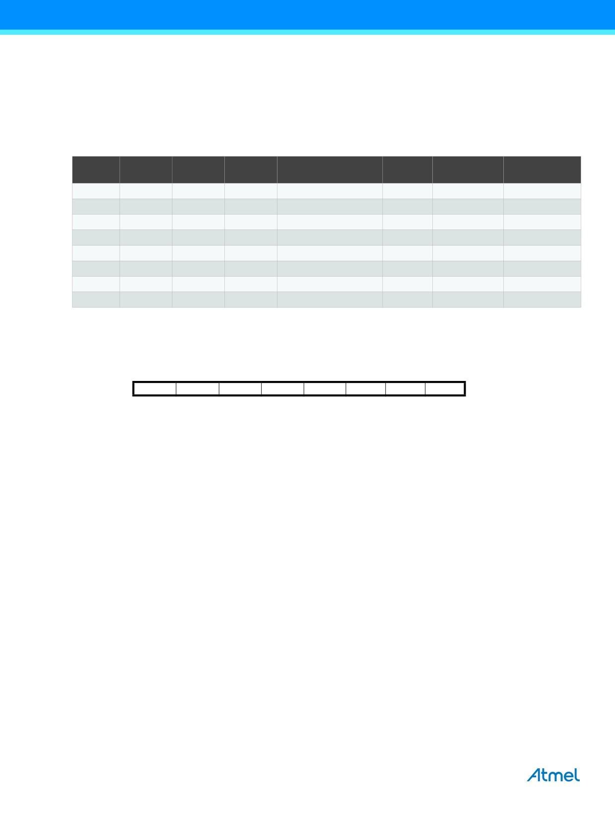
• Bits 1:0 - WGM21:0: Waveform Generation Mode
Combined with the WGM22 bit found in the TCCR2B register, these bits control the counting sequence of the counter, the
source for maximum (TOP) counter value, and what type of waveform generation to be used, see Table 17-8. Modes of
operation supported by the Timer/Counter unit are: Normal mode (counter), Clear timer on compare match (CTC) mode, and
two types of pulse width modulation (PWM) modes (see Section 17.7 “Modes of Operation” on page 120).
Table 17-8. Waveform Generation Mode Bit Description
Timer/Counter Mode of
Update of
TOV Flag
Mode
WGM2
WGM1
WGM0
Operation
TOP
OCRx at
Set on(1)(2)
0
0
0
0
Normal
0xFF
Immediate
MAX
1
0
0
1
PWM, phase correct
0xFF
TOP
BOTTOM
2
0
1
0
CTC
OCRA
Immediate
MAX
3
0
1
1
Fast PWM
0xFF
BOTTOM
MAX
4
1
0
0
Reserved
-
-
-
5
1
0
1
PWM, phase correct
OCRA
TOP
BOTTOM
6
1
1
0
Reserved
-
-
-
7
1
1
1
Fast PWM
OCRA
BOTTOM
TOP
Notes:
1.
MAX = 0xFF
2.
BOTTOM = 0x00
17.11.2 TCCR2B - Timer/Counter Control Register B
Bit
7
6
5
4
3
2
1
0
(0xB1)
FOC2A
FOC2B
-
-
WGM22
CS22
CS21
CS20
TCCR2B
Read/Write
W
W
R
R
R
R
R/W
R/W
Initial Value
0
0
0
0
0
0
0
0
• Bit 7 - FOC2A: Force Output Compare A
The FOC2A bit is only active when the WGM bits specify a non-PWM mode.
However, for ensuring compatibility with future devices, this bit must be set to zero when TCCR2B is written when operating
in PWM mode. When writing a logical one to the FOC2A bit, an immediate compare match is forced on the waveform
generation unit. The OC2A output is changed according to its COM2A1:0 bits setting. Note that the FOC2A bit is
implemented as a strobe. Therefore it is the value present in the COM2A1:0 bits that determines the effect of the forced
compare.
A FOC2A strobe will not generate any interrupt, nor will it clear the timer in CTC mode using OCR2A as TOP.
The FOC2A bit is always read as zero.
• Bit 6 - FOC2B: Force Output Compare B
The FOC2B bit is only active when the WGM bits specify a non-PWM mode.
However, for ensuring compatibility with future devices, this bit must be set to zero when TCCR2B is written when operating
in PWM mode. When writing a logical one to the FOC2B bit, an immediate compare match is forced on the waveform
generation unit. The OC2B output is changed according to its COM2B1:0 bits setting. Note that the FOC2B bit is
implemented as a strobe. Therefore it is the value present in the COM2B1:0 bits that determines the effect of the forced
compare.
A FOC2B strobe will not generate any interrupt, nor will it clear the timer in CTC mode using OCR2B as TOP.
The FOC2B bit is always read as zero.
• Bits 5:4 - Res: Reserved Bits
These bits are reserved bits in the ATmega328P and will always read as zero.
130
ATmega328P [DATASHEET]
7810D-AVR-01/15
• Bit 3 - WGM22: Waveform Generation Mode
See the description in the Section 17.11.1 “TCCR2A - Timer/Counter Control Register A” on page 127.
• Bit 2:0 - CS22:0: Clock Select
The three clock select bits select the clock source to be used by the Timer/Counter, see Table 17-9.
Table 17-9. Clock Select Bit Description
CS22
CS21
CS20
Description
0
0
0
No clock source (Timer/Counter stopped).
0
0
1
clkT2S/(no prescaling)
0
1
0
clkT2S/8 (from prescaler)
0
1
1
clkT2S/32 (from prescaler)
1
0
0
clkT2S/64 (from prescaler)
1
0
1
clkT2S/128 (from prescaler)
1
1
0
clkT2S/256 (from prescaler)
1
1
1
clkT2S/1024 (from prescaler)
If external pin modes are used for the Timer/Counter0, transitions on the T0 pin will clock the counter even if the pin is
configured as an output. This feature allows software control of the counting.
17.11.3 TCNT2 - Timer/Counter Register
Bit
7
6
5
4
3
2
1
0
(0xB2)
TCNT2[7:0]
TCNT2
Read/Write
R/W
R/W
R/W
R/W
R/W
R/W
R/W
R/W
Initial Value
0
0
0
0
0
0
0
0
The Timer/Counter register gives direct access, both for read and write operations, to the Timer/Counter unit 8-bit counter.
Writing to the TCNT2 register blocks (removes) the compare match on the following timer clock. Modifying the counter
(TCNT2) while the counter is running, introduces a risk of missing a compare match between TCNT2 and the OCR2x
registers.
17.11.4 OCR2A - Output Compare Register A
Bit
7
6
5
4
3
2
1
0
(0xB3)
OCR2A[7:0]
OCR2A
Read/Write
R/W
R/W
R/W
R/W
R/W
R/W
R/W
R/W
Initial Value
0
0
0
0
0
0
0
0
The output compare register A contains an 8-bit value that is continuously compared with the counter value (TCNT2). A
match can be used to generate an output compare interrupt, or to generate a waveform output on the OC2A pin.
17.11.5 OCR2B - Output Compare Register B
Bit
7
6
5
4
3
2
1
0
(0xB4)
OCR2B[7:0]
OCR2B
Read/Write
R/W
R/W
R/W
R/W
R/W
R/W
R/W
R/W
Initial Value
0
0
0
0
0
0
0
0
The output compare register B contains an 8-bit value that is continuously compared with the counter value (TCNT2). A
match can be used to generate an output compare interrupt, or to generate a waveform output on the OC2B pin.
ATmega328P [DATASHEET]
131
7810D-AVR-01/15
17.11.6 TIMSK2 - Timer/Counter2 Interrupt Mask Register
Bit
7
6
5
4
3
2
1
0
(0x70)
-
-
-
-
-
OCIE2B
OCIE2A
TOIE2
TIMSK2
Read/Write
R
R
R
R
R
R/W
R/W
R/W
Initial Value
0
0
0
0
0
0
0
0
• Bit 2 - OCIE2B: Timer/Counter2 Output Compare Match B Interrupt Enable
When the OCIE2B bit is written to one and the I-bit in the status register is set (one), the Timer/Counter2 compare match B
interrupt is enabled. The corresponding interrupt is executed if a compare match in Timer/Counter2 occurs, i.e., when the
OCF2B bit is set in the Timer/Counter 2 interrupt flag register - TIFR2.
• Bit 1 - OCIE2A: Timer/Counter2 Output Compare Match A Interrupt Enable
When the OCIE2A bit is written to one and the I-bit in the status register is set (one), the Timer/Counter2 compare match A
interrupt is enabled. The corresponding interrupt is executed if a compare match in Timer/Counter2 occurs, i.e., when the
OCF2A bit is set in the Timer/Counter 2 interrupt flag register - TIFR2.
• Bit 0 - TOIE2: Timer/Counter2 Overflow Interrupt Enable
When the TOIE2 bit is written to one and the I-bit in the status register is set (one), the Timer/Counter2 overflow interrupt is
enabled. The corresponding interrupt is executed if an overflow in Timer/Counter2 occurs, i.e., when the TOV2 bit is set in
the Timer/Counter2 interrupt flag register - TIFR2.
17.11.7 TIFR2 - Timer/Counter2 Interrupt Flag Register
Bit
7
6
5
4
3
2
1
0
0x17 (0x37)
-
-
-
-
-
OCF2B
OCF2A
TOV2
TIFR2
Read/Write
R
R
R
R
R
R/W
R/W
R/W
Initial Value
0
0
0
0
0
0
0
0
• Bit 2 - OCF2B: Output Compare Flag 2 B
The OCF2B bit is set (one) when a compare match occurs between the Timer/Counter2 and the data in OCR2B - output
compare register2. OCF2B is cleared by hardware when executing the corresponding interrupt handling vector.
Alternatively, OCF2B is cleared by writing a logic one to the flag. When the I-bit in SREG, OCIE2B (Timer/Counter2 compare
match interrupt enable), and OCF2B are set (one), the Timer/Counter2 compare match interrupt is executed.
• Bit 1 - OCF2A: Output Compare Flag 2 A
The OCF2A bit is set (one) when a compare match occurs between the Timer/Counter2 and the data in OCR2A - output
compare register2. OCF2A is cleared by hardware when executing the corresponding interrupt handling vector.
Alternatively, OCF2A is cleared by writing a logic one to the flag. When the I-bit in SREG, OCIE2A (Timer/Counter2 compare
match interrupt enable), and OCF2A are set (one), the Timer/Counter2 compare match interrupt is executed.
• Bit 0 - TOV2: Timer/Counter2 Overflow Flag
The TOV2 bit is set (one) when an overflow occurs in Timer/Counter2. TOV2 is cleared by hardware when executing the
corresponding interrupt handling vector. Alternatively, TOV2 is cleared by writing a logic one to the flag. When the
SREG I-bit, TOIE2A (Timer/Counter2 overflow interrupt enable), and TOV2 are set (one), the Timer/Counter2 overflow
interrupt is executed. In PWM mode, this bit is set when Timer/Counter2 changes counting direction at 0x00.
132
ATmega328P [DATASHEET]
7810D-AVR-01/15
17.11.8 ASSR - Asynchronous Status Register
Bit
7
6
5
4
3
2
1
0
(0xB6)
-
EXCLK
AS2
TCN2UB
OCR2AUB
OCR2BUB
TCR2AUB
TCR2BUB
ASSR
Read/Write
R
R/W
R/W
R
R
R
R
R
Initial Value
0
0
0
0
0
0
0
0
• Bit 7 - RES: Reserved bit
This bit is reserved and will always read as zero.
• Bit 6 - EXCLK: Enable External Clock Input
When EXCLK is written to one, and asynchronous clock is selected, the external clock input buffer is enabled and an
external clock can be input on timer oscillator 1 (TOSC1) pin instead of a 32kHz crystal. Writing to EXCLK should be done
before asynchronous operation is selected. Note that the crystal oscillator will only run when this bit is zero.
• Bit 5 - AS2: Asynchronous Timer/Counter2
When AS2 is written to zero, Timer/Counter2 is clocked from the I/O clock, clkI/O. When AS2 is written to one,
Timer/Counter2 is clocked from a crystal oscillator connected to the timer oscillator 1 (TOSC1) pin. When the value of AS2 is
changed, the contents of TCNT2, OCR2A, OCR2B, TCCR2A and TCCR2B might be corrupted.
• Bit 4 - TCN2UB: Timer/Counter2 Update Busy
When Timer/Counter2 operates asynchronously and TCNT2 is written, this bit becomes set. When TCNT2 has been
updated from the temporary storage register, this bit is cleared by hardware. A logical zero in this bit indicates that TCNT2 is
ready to be updated with a new value.
• Bit 3 - OCR2AUB: Output Compare Register2 Update Busy
When Timer/Counter2 operates asynchronously and OCR2A is written, this bit becomes set. When OCR2A has been
updated from the temporary storage register, this bit is cleared by hardware. A logical zero in this bit indicates that OCR2A is
ready to be updated with a new value.
• Bit 2 - OCR2BUB: Output Compare Register2 Update Busy
When Timer/Counter2 operates asynchronously and OCR2B is written, this bit becomes set. When OCR2B has been
updated from the temporary storage register, this bit is cleared by hardware. A logical zero in this bit indicates that OCR2B is
ready to be updated with a new value.
• Bit 1 - TCR2AUB: Timer/Counter Control Register2 Update Busy
When Timer/Counter2 operates asynchronously and TCCR2A is written, this bit becomes set. When TCCR2A has been
updated from the temporary storage register, this bit is cleared by hardware. A logical zero in this bit indicates that TCCR2A
is ready to be updated with a new value.
ATmega328P [DATASHEET]
133
7810D-AVR-01/15
• Bit 0 - TCR2BUB: Timer/Counter Control Register2 Update Busy
When Timer/Counter2 operates asynchronously and TCCR2B is written, this bit becomes set. When TCCR2B has been
updated from the temporary storage register, this bit is cleared by hardware. A logical zero in this bit indicates that TCCR2B
is ready to be updated with a new value.
If a write is performed to any of the five Timer/Counter2 registers while its update busy flag is set, the updated value might
get corrupted and cause an unintentional interrupt to occur.
The mechanisms for reading TCNT2, OCR2A, OCR2B, TCCR2A and TCCR2B are different. When reading TCNT2, the
actual timer value is read. When reading OCR2A, OCR2B, TCCR2A and TCCR2B the value in the temporary storage
register is read.
17.11.9 GTCCR - General Timer/Counter Control Register
Bit
7
6
5
4
3
2
1
0
0x23 (0x43)
TSM
-
-
-
-
-
PSRASY
PSRSYNC
GTCCR
Read/Write
R/W
R
R
R
R
R
R/W
R/W
Initial Value
0
0
0
0
0
0
0
0
• Bit 1 - PSRASY: Prescaler Reset Timer/Counter2
When this bit is one, the Timer/Counter2 prescaler will be reset. This bit is normally cleared immediately by hardware. If the
bit is written when Timer/Counter2 is operating in asynchronous mode, the bit will remain one until the prescaler has been
reset. The bit will not be cleared by hardware if the TSM bit is set. Refer to the description of “Bit 7 - TSM: Timer/Counter
Synchronization Mode” on page 115 for a description of the Timer/Counter synchronization mode.
134
ATmega328P [DATASHEET]
7810D-AVR-01/15
18.
SPI - Serial Peripheral Interface
18.1
Features
● Full-duplex, three-wire synchronous data transfer
● Master or slave operation
● LSB first or MSB first data transfer
● Seven programmable bit rates
● End of transmission interrupt flag
● Write collision flag protection
● Wake-up from idle mode
● Double speed (CK/2) master SPI mode
18.2
Overview
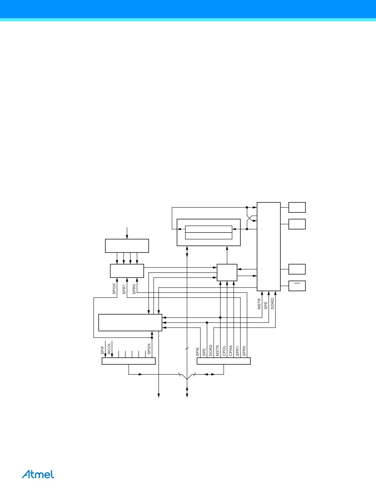
The serial peripheral interface (SPI) allows high-speed synchronous data transfer between the ATmega328P and peripheral
devices or between several AVR® devices.
The USART can also be used in master SPI mode, see Section 20. “USART in SPI Mode” on page 166. The PRSPI bit in
Section 9.10 “Minimizing Power Consumption” on page 36 must be written to zero to enable SPI module.
Figure 18-1. SPI Block Diagram(1)
S
MISO
M
MSB
LSB
M
XTAL
MOSI
8 Bit Shift Register
S
Read Data Buffer
Pin
Divider
Control
/2/4/8/16/32/64/128
Logic
Clock
SPI Clock (Master)
Clock
S
SCK
Select
Logic
M
SS
MSTR
SPE
SPI Control
8
SPI Status Register
SPI Control Register
8
8
SPI Interrupt
Internal
Request
Data Bus
Note:
1.
Refer to Figure 1-1 on page 3, and Table 13-3 on page 65 for SPI pin placement.
ATmega328P [DATASHEET]
135
7810D-AVR-01/15
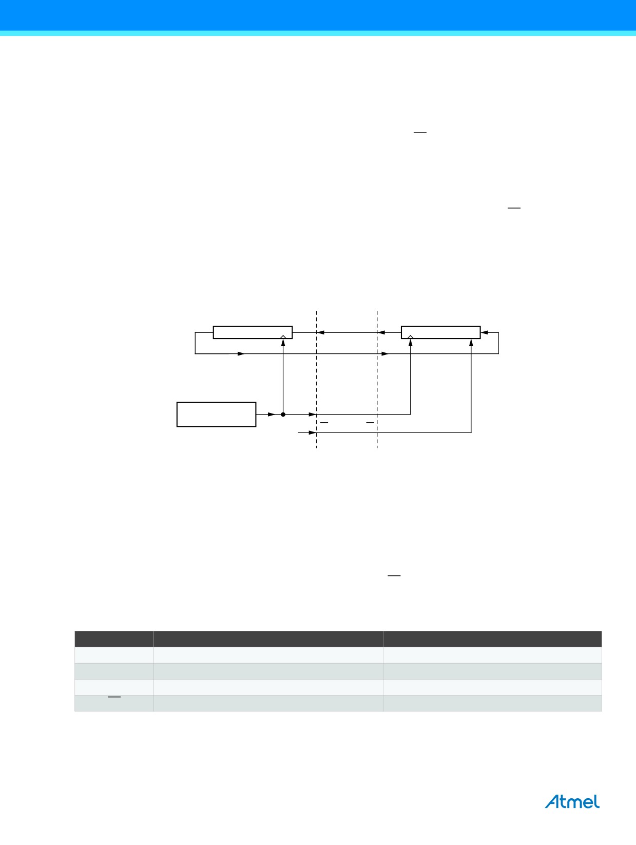
The interconnection between master and slave CPUs with SPI is shown in Figure 18-2. The system consists of two shift
registers, and a master clock generator. The SPI master initiates the communication cycle when pulling low the slave select
SS pin of the desired slave. master and slave prepare the data to be sent in their respective shift registers, and the master
generates the required clock pulses on the SCK line to interchange data. Data is always shifted from master to slave on the
master out - slave In, MOSI, line, and from slave to master on the master In - slave out, MISO, line. After each data packet,
the master will synchronize the Slave by pulling high the slave select, SS, line.
When configured as a master, the SPI interface has no automatic control of the SS line. This must be handled by user
software before communication can start. When this is done, writing a byte to the SPI data register starts the SPI clock
generator, and the hardware shifts the eight bits into the Slave. After shifting one byte, the SPI clock generator stops, setting
the end of transmission flag (SPIF). If the SPI interrupt enable bit (SPIE) in the SPCR register is set, an interrupt is
requested. The master may continue to shift the next byte by writing it into SPDR, or signal the end of packet by pulling high
the slave select, SS line. The last incoming byte will be kept in the buffer register for later use.
When configured as a slave, the SPI interface will remain sleeping with MISO tri-stated as long as the SS pin is driven high.
In this state, software may update the contents of the SPI data register, SPDR, but the data will not be shifted out by
incoming clock pulses on the SCK pin until the SS pin is driven low. As one byte has been completely shifted, the end of
transmission flag, SPIF is set. If the SPI interrupt enable bit, SPIE, in the SPCR register is set, an interrupt is requested. The
slave may continue to place new data to be sent into SPDR before reading the incoming data. The last incoming byte will be
kept in the buffer register for later use.
Figure 18-2. SPI Master-slave Interconnection
MSB MASTER
LSB
MISO
MISO
MSB SLAVE LSB
8 Bit Shift Register
8 Bit Shift Register
MOSI
MOSI
Shift
SCK
SCK
Enable
SPI
Clock Generator
SS
SS
The system is single buffered in the transmit direction and double buffered in the receive direction. This means that bytes to
be transmitted cannot be written to the SPI data register before the entire shift cycle is completed. When receiving data,
however, a received character must be read from the SPI data register before the next character has been completely
shifted in. Otherwise, the first byte is lost.
In SPI slave mode, the control logic will sample the incoming signal of the SCK pin. To ensure correct sampling of the clock
signal, the minimum low and high periods should be:
Low periods: Longer than 2 CPU clock cycles.
High periods: Longer than 2 CPU clock cycles.
When the SPI is enabled, the data direction of the MOSI, MISO, SCK, and SS pins is overridden according to Table 18-1. For
more details on automatic port overrides, refer to Section 13.3 “Alternate Port Functions” on page 63.
Table 18-1. SPI Pin Overrides(1)
Pin
Direction, Master SPI
Direction, Slave SPI
MOSI
User defined
Input
MISO
Input
User defined
SCK
User defined
Input
SS
User defined
Input
Note:
1.
See Section 13.3.1 “Alternate Functions of Port B” on page 65 for a detailed description of how to define the
direction of the user defined SPI pins.
136
ATmega328P [DATASHEET]
7810D-AVR-01/15

The following code examples show how to initialize the SPI as a master and how to perform a simple transmission.
DDR_SPI in the examples must be replaced by the actual data direction register controlling the SPI pins. DD_MOSI,
DD_MISO and DD_SCK must be replaced by the actual data direction bits for these pins. E.g. if MOSI is placed on pin PB5,
replace DD_MOSI with DDB5 and DDR_SPI with DDRB.
Assembly Code Example(1)
SPI_MasterInit:
; Set MOSI and SCK output, all others input
ldi
r17,(1<<DD_MOSI)|(1<<DD_SCK)
out
DDR_SPI,r17
; Enable SPI, Master, set clock rate fck/16
ldi
r17,(1<<SPE)|(1<<MSTR)|(1<<SPR0)
out
SPCR,r17
ret
SPI_MasterTransmit:
; Start transmission of data (r16)
out
SPDR,r16
Wait_Transmit:
; Wait for transmission complete
in
r16, SPSR
sbrs
r16, SPIF
rjmp
Wait_Transmit
ret
C Code Example(1)
void SPI_MasterInit(void)
{
/* Set MOSI and SCK output, all others input */
DDR_SPI = (1<<DD_MOSI)|(1<<DD_SCK);
/* Enable SPI, Master, set clock rate fck/16 */
SPCR = (1<<SPE)|(1<<MSTR)|(1<<SPR0);
}
void SPI_MasterTransmit(char cData)
{
/* Start transmission */
SPDR = cData;
/* Wait for transmission complete */
while(!(SPSR & (1<<SPIF)))
;
}
Note:
1.
See Section 5. “About Code Examples” on page 8.
ATmega328P [DATASHEET]
137
7810D-AVR-01/15
The following code examples show how to initialize the SPI as a Slave and how to perform a simple reception.
Assembly Code Example(1)
SPI_SlaveInit:
; Set MISO output, all others input
ldi
r17,(1<<DD_MISO)
out
DDR_SPI,r17
; Enable SPI
ldi
r17,(1<<SPE)
out
SPCR,r17
ret
SPI_SlaveReceive:
; Wait for reception complete
sbis SPSR,SPIF
rjmp SPI_SlaveReceive
; Read received data and return
in
r16,SPDR
ret
C Code Example(1)
void SPI_SlaveInit(void)
{
/* Set MISO output, all others input */
DDR_SPI = (1<<DD_MISO);
/* Enable SPI */
SPCR = (1<<SPE);
}
char SPI_SlaveReceive(void)
{
/* Wait for reception complete */
while(!(SPSR & (1<<SPIF)))
;
/* Return Data Register */
return SPDR;
}
Note:
1.
See Section 5. “About Code Examples” on page 8.
18.3
SS Pin Functionality
18.3.1
Slave Mode
When the SPI is configured as a slave, the slave select (SS) pin is always input. When SS is held low, the SPI is activated,
and MISO becomes an output if configured so by the user. All other pins are inputs. When SS is driven high, all pins are
inputs, and the SPI is passive, which means that it will not receive incoming data. Note that the SPI logic will be reset once
the SS pin is driven high.
The SS pin is useful for packet/byte synchronization to keep the slave bit counter synchronous with the master clock
generator. When the SS pin is driven high, the SPI slave will immediately reset the send and receive logic, and drop any
partially received data in the shift register.
138
ATmega328P [DATASHEET]
7810D-AVR-01/15
18.3.2
Master Mode
When the SPI is configured as a master (MSTR in SPCR is set), the user can determine the direction of the SS pin.
If SS is configured as an output, the pin is a general output pin which does not affect the SPI system. Typically, the pin will be
driving the SS pin of the SPI slave.
If SS is configured as an input, it must be held high to ensure master SPI operation. If the SS pin is driven low by peripheral
circuitry when the SPI is configured as a master with the SS pin defined as an input, the SPI system interprets this as
another master selecting the SPI as a slave and starting to send data to it. To avoid bus contention, the SPI system takes the
following actions:
1.
The MSTR bit in SPCR is cleared and the SPI system becomes a slave. As a result of the SPI becoming a slave,
the MOSI and SCK pins become inputs.
2.
The SPIF flag in SPSR is set, and if the SPI interrupt is enabled, and the I-bit in SREG is set, the interrupt routine
will be executed.
Thus, when interrupt-driven SPI transmission is used in master mode, and there exists a possibility that SS is driven low, the
interrupt should always check that the MSTR bit is still set. If the MSTR bit has been cleared by a slave select, it must be set
by the user to re-enable SPI master mode.
18.4
Data Modes
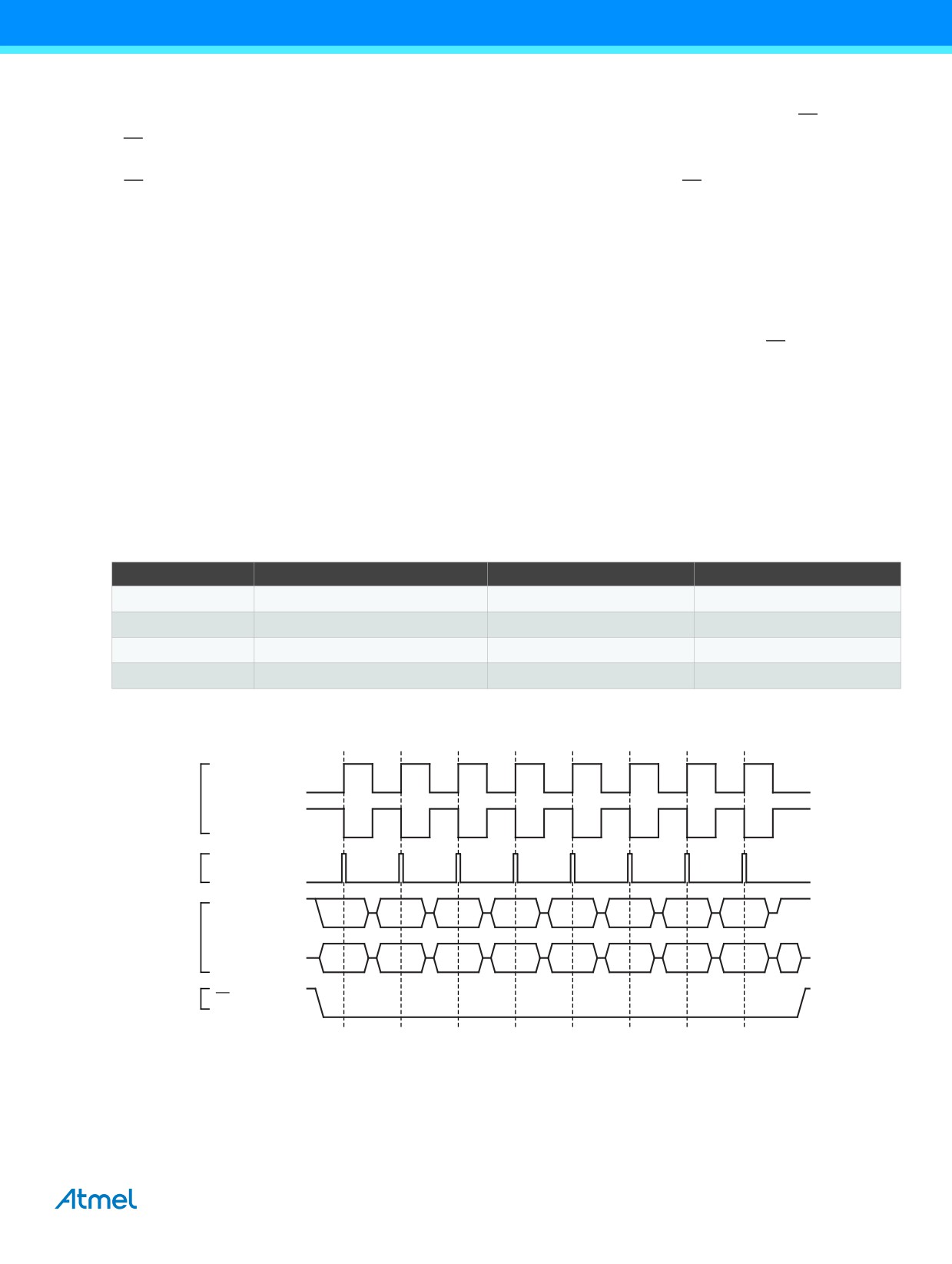
There are four combinations of SCK phase and polarity with respect to serial data, which are determined by control bits
CPHA and CPOL. The SPI data transfer formats are shown in Figure 18-3 and Figure 18-4 on page 140. Data bits are
shifted out and latched in on opposite edges of the SCK signal, ensuring sufficient time for data signals to stabilize. This is
clearly seen by summarizing Table 18-3 on page 140 and Table 18-4 on page 141, as done in Table 18-2.
Table 18-2. SPI Modes
SPI Mode
Conditions
Leading Edge
Trailing eDge
0
CPOL=0, CPHA=0
Sample (rising)
Setup (falling)
1
CPOL=0, CPHA=1
Setup (rising)
Sample (falling)
2
CPOL=1, CPHA=0
Sample (falling)
Setup (rising)
3
CPOL=1, CPHA=1
Setup (falling)
Sample (rising)
Figure 18-3. SPI Transfer Format with CPHA=0
SCK (CPOL = 0)
mode 0
SCK (CPOL = 1)
mode 2
SAMPLE I
MOSI/MISO
CHANGE 0
MOSI PIN
CHANGE 0
MISO PIN
SS
MSB first (DORD = 0) MSB
Bit 6
Bit 5
Bit 4
Bit 3
Bit 2
Bit 1
LSB
LSB first (DORD =1)
LSB
Bit 1
Bit 2
Bit 3
Bit 4
Bit 5
Bit 6
MSB
ATmega328P [DATASHEET]
139
7810D-AVR-01/15
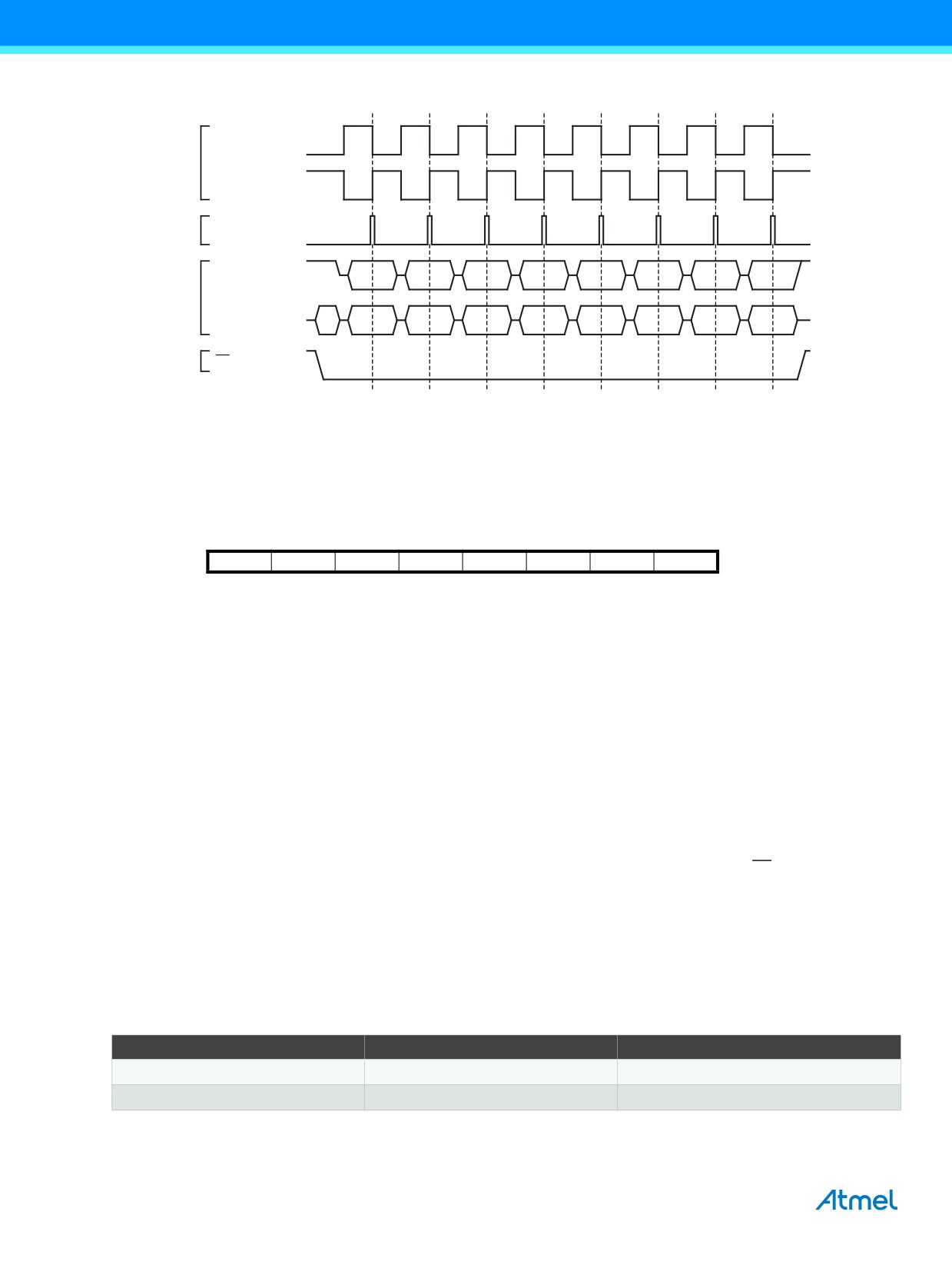
Figure 18-4. SPI Transfer Format with CPHA=1
SCK (CPOL = 0)
mode 1
SCK (CPOL = 1)
mode 3
SAMPLE I
MOSI/MISO
CHANGE 0
MOSI PIN
CHANGE 0
MISO PIN
SS
MSB first (DORD = 0)
MSB
Bit 6
Bit 5
Bit 4
Bit 3
Bit 2
Bit 1
LSB
LSB first (DORD =1)
LSB
Bit 1
Bit 2
Bit 3
Bit 4
Bit 5
Bit 6
MSB
18.5
Register Description
18.5.1
SPCR - SPI Control Register
Bit
7
6
5
4
3
2
1
0
0x2C (0x4C)
SPIE
SPE
DORD
MSTR
CPOL
CPHA
SPR1
SPR0
SPCR
Read/Write
R/W
R/W
R/W
R/W
R/W
R/W
R/W
R/W
Initial Value
0
0
0
0
0
0
0
0
• Bit 7 - SPIE: SPI Interrupt Enable
This bit causes the SPI interrupt to be executed if SPIF bit in the SPSR register is set and the if the global interrupt enable bit
in SREG is set.
• Bit 6 - SPE: SPI Enable
When the SPE bit is written to one, the SPI is enabled. This bit must be set to enable any SPI operations.
• Bit 5 - DORD: Data Order
When the DORD bit is written to one, the LSB of the data word is transmitted first.
When the DORD bit is written to zero, the MSB of the data word is transmitted first.
• Bit 4 - MSTR: Master/Slave Select
This bit selects master SPI mode when written to one, and slave SPI mode when written logic zero. If SS is configured as an
input and is driven low while MSTR is set, MSTR will be cleared, and SPIF in SPSR will become set. The user will then have
to set MSTR to re-enable SPI master mode.
• Bit 3 - CPOL: Clock Polarity
When this bit is written to one, SCK is high when idle. When CPOL is written to zero, SCK is low when idle. Refer to Figure
18-3 on page 139 and Figure 18-4 for an example. The CPOL functionality is summarized below.
Table 18-3. CPOL Functionality
CPOL
Leading Edge
Trailing Edge
0
Rising
Falling
1
Falling
Rising
140
ATmega328P [DATASHEET]
7810D-AVR-01/15
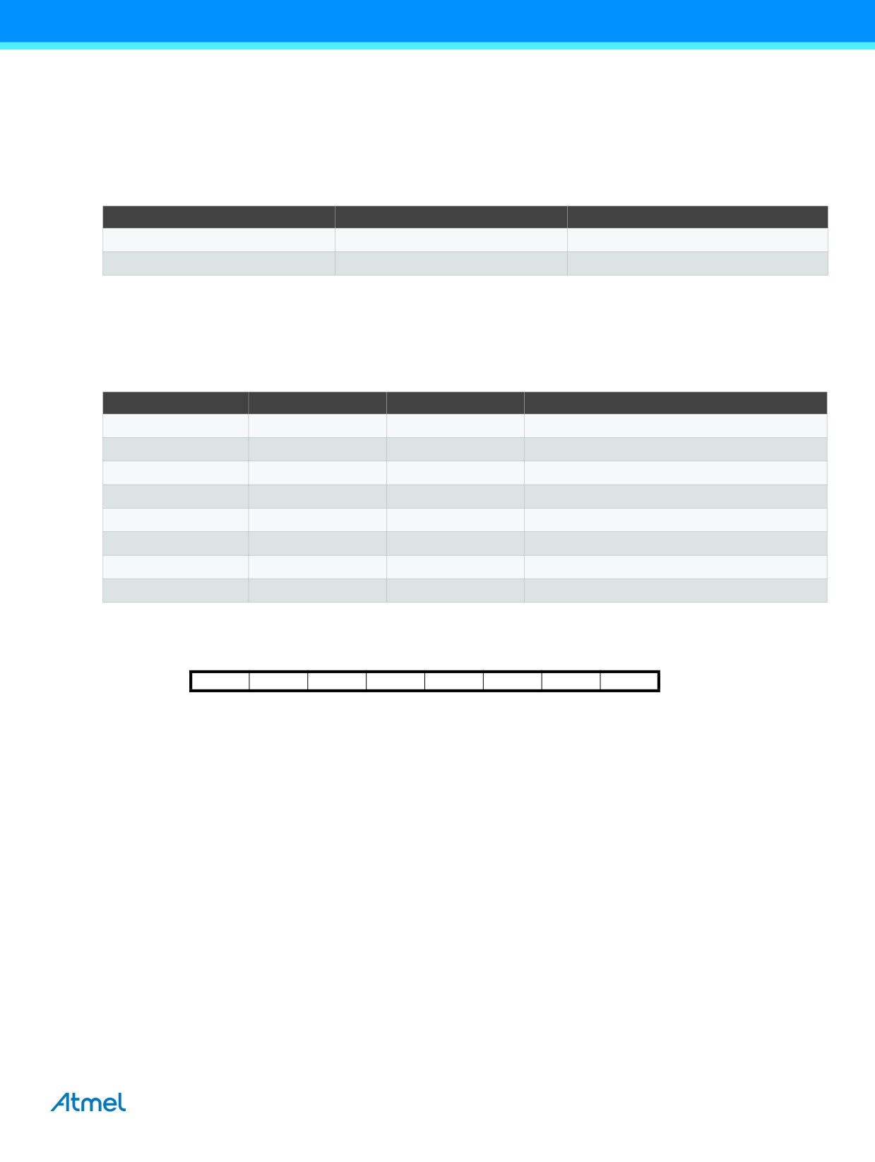
• Bit 2 - CPHA: Clock Phase
The settings of the clock phase bit (CPHA) determine if data is sampled on the leading (first) or trailing (last) edge of SCK.
Refer to Figure 18-3 on page 139 and Figure 18-4 on page 140 for an example. The CPOL functionality is summarized
below:
Table 18-4. CPHA Functionality
CPHA
Leading Edge
Trailing Edge
0
Sample
Setup
1
Setup
Sample
• Bits 1, 0 - SPR1, SPR0: SPI Clock Rate Select 1 and 0
These two bits control the SCK rate of the device configured as a master. SPR1 and SPR0 have no effect on the slave.
The relationship between SCK and the oscillator clock frequency fosc is shown in Table 18-5.
Table 18-5. Relationship Between SCK and the Oscillator Frequency
SPI2X
SPR1
SPR0
SCK Frequency
0
0
0
fosc/4
0
0
1
fosc/16
0
1
0
fosc/64
0
1
1
fosc/128
1
0
0
fosc/2
1
0
1
fosc/8
1
1
0
fosc/32
1
1
1
fosc/64
18.5.2
SPSR - SPI Status Register
Bit
7
6
5
4
3
2
1
0
0x2D (0x4D)
SPIF
WCOL
-
-
-
-
-
SPI2X
SPSR
Read/Write
R
R
R
R
R
R
R
R/W
Initial Value
0
0
0
0
0
0
0
0
• Bit 7 - SPIF: SPI Interrupt Flag
When a serial transfer is complete, the SPIF Flag is set. An interrupt is generated if SPIE in SPCR is set and global
interrupts are enabled. If SS is an input and is driven low when the SPI is in master mode, this will also set the SPIF flag.
SPIF is cleared by hardware when executing the corresponding interrupt handling vector. Alternatively, the SPIF bit is
cleared by first reading the SPI status register with SPIF set, then accessing the SPI data register (SPDR).
• Bit 6 - WCOL: Write COLlision Flag
The WCOL bit is set if the SPI data register (SPDR) is written during a data transfer. The WCOL bit (and the SPIF bit) are
cleared by first reading the SPI status register with WCOL set, and then accessing the SPI data register.
ATmega328P [DATASHEET]
141
7810D-AVR-01/15
• Bit 5..1 - Res: Reserved Bits
These bits are reserved bits in the Atmel® ATmega328P and will always read as zero.
• Bit 0 - SPI2X: Double SPI Speed Bit
When this bit is written logic one the SPI speed (SCK frequency) will be doubled when the SPI is in master mode
(see Table 18-5 on page 141). This means that the minimum SCK period will be two CPU clock periods. When the SPI is
configured as slave, the SPI is only guaranteed to work at fosc/4 or lower.
The SPI interface on the Atmel ATmega328P is also used for program memory and EEPROM downloading or uploading.
See Section 27.8 “Serial Downloading” on page 254 for serial programming and verification.
18.5.3
SPDR - SPI Data Register
Bit
7
6
5
4
3
2
1
0
0x2E (0x4E)
MSB
LSB
SPDR
Read/Write
R/W
R/W
R/W
R/W
R/W
R/W
R/W
R/W
Initial Value
X
X
X
X
X
X
X
X
Undefined
The SPI data register is a read/write register used for data transfer between the register file and the SPI shift register. Writing
to the register initiates data transmission. Reading the register causes the shift register Receive buffer to be read.
142
ATmega328P [DATASHEET]
7810D-AVR-01/15
19.
USART0
19.1
Features
● Full duplex operation (independent serial receive and transmit registers)
● Asynchronous or synchronous operation
● Master or slave clocked synchronous operation
● High resolution baud rate generator
● Supports serial frames with 5, 6, 7, 8, or 9 data bits and 1 or 2 stop bits
● Odd or even parity generation and parity check supported by hardware
● Data overrun detection
● Framing error detection
● Noise filtering includes false start bit detection and digital low pass filter
● Three separate interrupts on TX complete, TX data register empty and RX complete
● Multi-processor communication mode
● Double speed asynchronous communication mode
19.2
Overview
The universal synchronous and asynchronous serial receiver and transmitter (USART) is a highly flexible serial
communication device.
The USART0 can also be used in master SPI mode, see Section 20. “USART in SPI Mode” on page 166. The power
reduction USART bit, PRUSART0, in Section 9.10 “Minimizing Power Consumption” on page 36 must be disabled by writing
a logical zero to it.
A simplified block diagram of the USART transmitter is shown in Figure 19-1 on page 144. CPU accessible I/O registers and
I/O pins are shown in bold.
The dashed boxes in the block diagram separate the three main parts of the USART (listed from the top): Clock generator,
transmitter and receiver. Control registers are shared by all units. The clock generation logic consists of synchronization
logic for external clock input used by synchronous slave operation, and the baud rate generator. The XCKn (transfer clock)
pin is only used by synchronous transfer mode. The transmitter consists of a single write buffer, a serial shift register, parity
generator and control logic for handling different serial frame formats. The write buffer allows a continuous transfer of data
without any delay between frames. The receiver is the most complex part of the USART module due to its clock and data
recovery units. The recovery units are used for asynchronous data reception. In addition to the recovery units, the receiver
includes a parity checker, control logic, a shift register and a two level receive buffer (UDRn). The receiver supports the
same frame formats as the transmitter, and can detect frame error, data overrun and parity errors.
ATmega328P [DATASHEET]
143
7810D-AVR-01/15
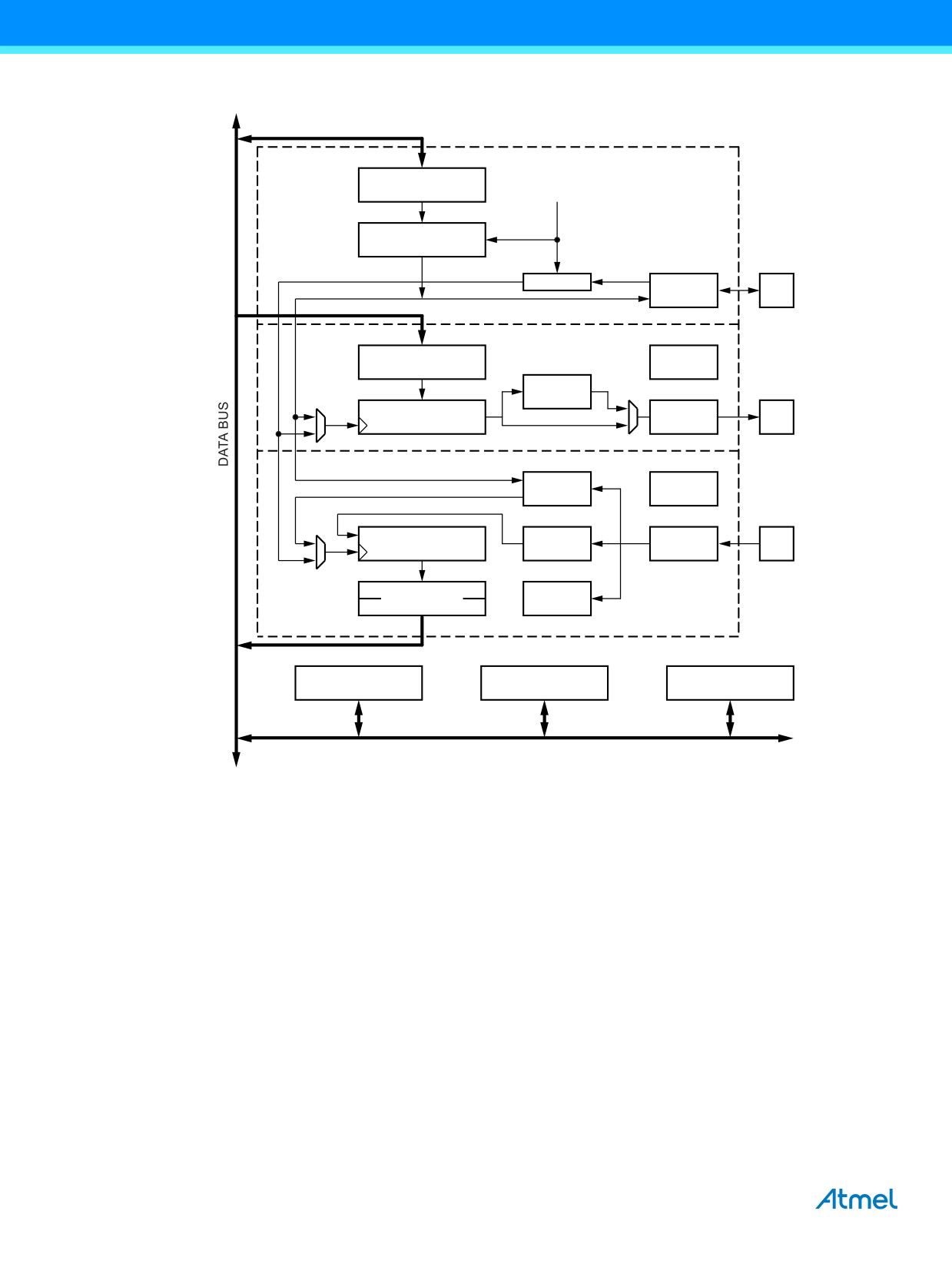
Figure 19-1. USART Block Diagram(1)
Clock Generator
UBRRn [H:L]
OSC
Baud Rate Generator
Sync Logic
Pin
XCKn
Control
Transmitter
TX
UDRn (Transmit)
Control
Parity
Generator
Pin
Transmit Shift Register
TxDn
Control
Receiver
Clock
RX
Recovery
Control
Data
Pin
Receive Shift Register
RxDn
Recovery
Control
Parity
UDRn (Receive)
Checker
UCSRnA
UCSRnB
UCSRnC
Note:
1.
Refer to Figure 1-1 on page 3 and Table 13-9 on page 70 for USART0 pin placement.
19.3
Clock Generation
The clock generation logic generates the base clock for the transmitter and receiver. The USART supports four modes of
clock operation: Normal asynchronous, double speed asynchronous, master synchronous and slave synchronous mode.
The UMSELn bit in USART control and status register C (UCSRnC) selects between asynchronous and synchronous
operation. Double speed (asynchronous mode only) is controlled by the U2Xn found in the UCSRnA register. When using
synchronous mode (UMSELn = 1), the data direction register for the XCKn pin (DDR_XCKn) controls whether the clock
source is internal (master mode) or external (slave mode). The XCKn pin is only active when using synchronous mode.
144
ATmega328P [DATASHEET]
7810D-AVR-01/15
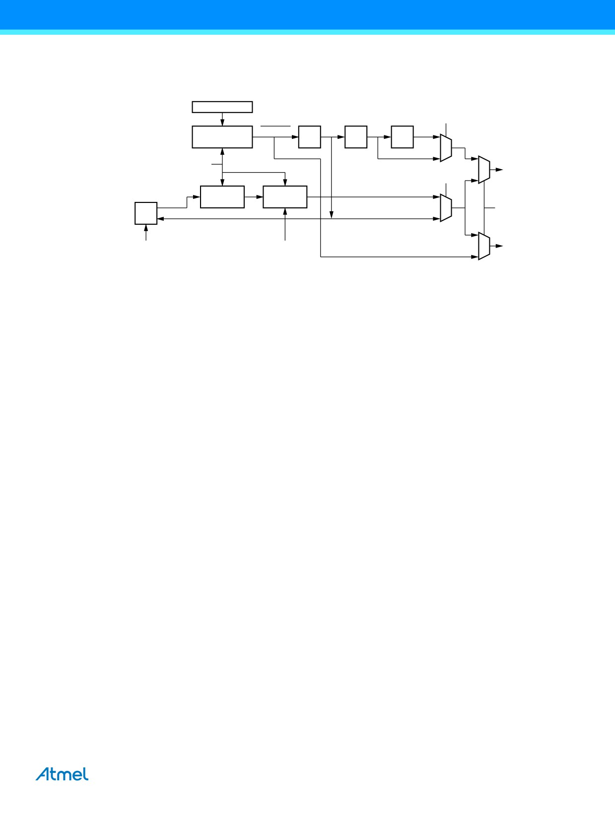
Figure 19-2 shows a block diagram of the clock generation logic.
Figure 19-2. Clock Generation Logic, Block Diagram
UBRRn
U2Xn
foscn
Prescaling
UBRRn+1
/2
/4
/2
Down-Counter
0
1
OSC
0
txclk
DDR_XCKn
1
Sync
Edge
xcki
Register
Detector
0
XCKn
UMSELn
xcko
1
Pin
0
DDR_XCKn
UCPOLn
rxclk
1
Signal description:
txclk
Transmitter clock (Internal Signal).
rxclk
Receiver base clock (Internal Signal).
xcki
Input from XCK pin (internal Signal). Used for synchronous slave operation.
xcko Clock output to XCK pin (Internal Signal). Used for synchronous master operation.
fosc
XTAL pin frequency (System Clock).
19.3.1
Internal Clock Generation - The Baud Rate Generator
Internal clock generation is used for the asynchronous and the synchronous master modes of operation. The description in
this section refers to Figure 19-2.
The USART baud rate register (UBRRn) and the down-counter connected to it function as a programmable prescaler or
baud rate generator. The down-counter, running at system clock (fosc), is loaded with the UBRRn value each time the
counter has counted down to zero or when the UBRRnL register is written. A clock is generated each time the counter
reaches zero. This clock is the baud rate generator clock output (= fosc/(UBRRn+1)). The transmitter divides the baud rate
generator clock output by 2, 8 or 16 depending on mode. The baud rate generator output is used directly by the receiver’s
clock and data recovery units. However, the recovery units use a state machine that uses 2, 8 or 16 states depending on
mode set by the state of the UMSELn, U2Xn and DDR_XCKn bits.
ATmega328P [DATASHEET]
145
7810D-AVR-01/15
Table 19-1 contains equations for calculating the baud rate (in bits per second) and for calculating the UBRRn value for each
mode of operation using an internally generated clock source.
Table 19-1. Equations for Calculating Baud Rate Register Setting
Equation for Calculating UBRRn
Operating Mode
Equation for Calculating Baud Rate(1)
Value
fOSC
fOSC
Asynchronous normal mode (U2Xn = 0)
BAUD
= ---------------------------------------
UBRRn
= ---------------------- - 1
16UBRRn + 1
16BAUD
Asynchronous double speed mode
fOSC
fOSC
(U2Xn = 1)
BAUD
= ------------------------------------
UBRRn
= ------------------- - 1
8UBRRn + 1
8BAUD
fOSC
fOSC
Synchronous master mode
BAUD
= ------------------------------------
UBRRn
= ------------------- - 1
8UBRRn + 1
2BAUD
Note:
1.
The baud rate is defined to be the transfer rate in bit per second (bps)
BAUD
Baud rate (in bits per second, bps)
fOSC
System oscillator clock frequency
UBRRn
Contents of the UBRRnH and UBRRnL registers, (0-4095)
Some examples of UBRRn values for some system clock frequencies are found in Table 19-9 on page 163.
19.3.2
Double Speed Operation (U2Xn)
The transfer rate can be doubled by setting the U2Xn bit in UCSRnA. Setting this bit only has effect for the asynchronous
operation. Set this bit to zero when using synchronous operation.
Setting this bit will reduce the divisor of the baud rate divider from 16 to 8, effectively doubling the transfer rate for
asynchronous communication. Note however that the receiver will in this case only use half the number of samples (reduced
from 16 to 8) for data sampling and clock recovery, and therefore a more accurate baud rate setting and system clock are
required when this mode is used. For the transmitter, there are no downsides.
19.3.3
External Clock
External clocking is used by the synchronous slave modes of operation. The description in this section refers to Figure 19-2
on page 145 for details.
External clock input from the XCKn pin is sampled by a synchronization register to minimize the chance of meta-stability.
The output from the synchronization register must then pass through an edge detector before it can be used by the
transmitter and receiver. This process introduces a two CPU clock period delay and therefore the maximum external XCKn
clock frequency is limited by the following equation:
fOSC
fXCK
----------
4
Note that fosc depends on the stability of the system clock source. It is therefore recommended to add some margin to avoid
possible loss of data due to frequency variations.
146
ATmega328P [DATASHEET]
7810D-AVR-01/15
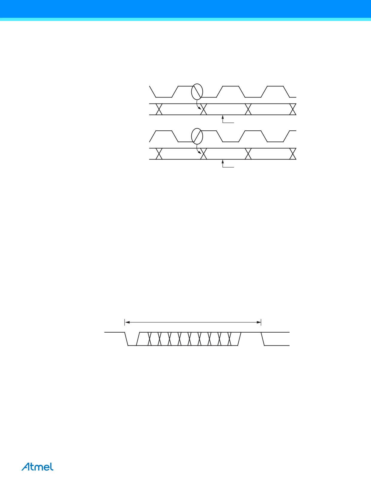
19.3.4
Synchronous Clock Operation
When synchronous mode is used (UMSELn = 1), the XCKn pin will be used as either clock input (Slave) or clock output
(master). The dependency between the clock edges and data sampling or data change is the same. The basic principle is
that data input (on RxDn) is sampled at the opposite XCKn clock edge of the edge the data output (TxDn) is changed.
Figure 19-3. Synchronous Mode XCKn Timing
UCPOL = 1
XCK
RxD/ TxD
Sample
UCPOL = 0
XCK
RxD/ TxD
Sample
The UCPOLn bit UCRSC selects which XCKn clock edge is used for data sampling and which is used for data change. As
Figure 19-3 shows, when UCPOLn is zero the data will be changed at rising XCKn edge and sampled at falling XCKn edge.
If UCPOLn is set, the data will be changed at falling XCKn edge and sampled at rising XCKn edge.
19.4
Frame Formats
A serial frame is defined to be one character of data bits with synchronization bits (start and stop bits), and optionally a parity
bit for error checking. The USART accepts all 30 combinations of the following as valid frame formats:
●
1 start bit
●
5, 6, 7, 8, or 9 data bits
● no, even or odd parity bit
●
1 or 2 stop bits
A frame starts with the start bit followed by the least significant data bit. Then the next data bits, up to a total of nine, are
succeeding, ending with the most significant bit. If enabled, the parity bit is inserted after the data bits, before the stop bits.
When a complete frame is transmitted, it can be directly followed by a new frame, or the communication line can be set to an
idle (high) state. Figure 19-4 illustrates the possible combinations of the frame formats. Bits inside brackets are optional.
Figure 19-4. Frame Formats
FRAME
(IDLE)
ST
0
1
2
3
4
[5]
[6]
[7]
[8]
[P] Sp1 [Sp2]
(St/IDLE)
St
Start bit, always low.
(n)
Data bits (0 to 8).
P
Parity bit. Can be odd or even.
Sp
Stop bit, always high.
IDLE No transfers on the communication line (RxDn or TxDn). An IDLE line must be high.
ATmega328P [DATASHEET]
147
7810D-AVR-01/15
The frame format used by the USART is set by the UCSZn2:0, UPMn1:0 and USBSn bits in UCSRnB and UCSRnC. The
receiver and transmitter use the same setting. Note that changing the setting of any of these bits will corrupt all ongoing
communication for both the receiver and transmitter.
The USART character size (UCSZn2:0) bits select the number of data bits in the frame. The USART parity mode (UPMn1:0)
bits enable and set the type of parity bit. The selection between one or two stop bits is done by the USART stop bit select
(USBSn) bit. The receiver ignores the second stop bit. An FE (frame error) will therefore only be detected in the cases where
the first stop bit is zero.
19.4.1
Parity Bit Calculation
The parity bit is calculated by doing an exclusive-or of all the data bits. If odd parity is used, the result of the exclusive or is
inverted. The relation between the parity bit and data bits is as follows:
Peven
=
dn-1
d3
d2
d1
d0
0
Podd = dn-1
d3
d2
d1
d0
1
Peven
Parity bit using even parity
Podd
Parity bit using odd parity
dn
Data bit n of the character
If used, the parity bit is located between the last data bit and first stop bit of a serial frame.
19.5
USART Initialization
The USART has to be initialized before any communication can take place. The initialization process normally consists of
setting the baud rate, setting frame format and enabling the transmitter or the receiver depending on the usage. For interrupt
driven USART operation, the global interrupt flag should be cleared (and interrupts globally disabled) when doing the
initialization.
Before doing a re-initialization with changed baud rate or frame format, be sure that there are no ongoing transmissions
during the period the registers are changed. The TXCn flag can be used to check that the transmitter has completed all
transfers, and the RXC flag can be used to check that there are no unread data in the receive buffer. Note that the TXCn flag
must be cleared before each transmission (before UDRn is written) if it is used for this purpose.
148
ATmega328P [DATASHEET]
7810D-AVR-01/15
The following simple USART initialization code examples show one assembly and one C function that are equal in
functionality. The examples assume asynchronous operation using polling (no interrupts enabled) and a fixed frame format.
The baud rate is given as a function parameter. For the assembly code, the baud rate parameter is assumed to be stored in
the r17:r16 registers.
Assembly Code Example(1)
USART_Init:
; Set baud rate
out
UBRRnH, r17
out
UBRRnL, r16
; Enable receiver and transmitter
ldi
r16, (1<<RXENn)|(1<<TXENn)
out
UCSRnB,r16
; Set frame format: 8data, 2stop bit
ldi
r16, (1<<USBSn)|(3<<UCSZn0)
out
UCSRnC,r16
ret
C Code Example(1)
#define FOSC 1843200 // Clock Speed
#define BAUD 9600
#define MYUBRR FOSC/16/BAUD-1
void main(void)
{
USART_Init(MYUBRR)
}
void USART_Init(unsigned int ubrr)
{
/*Set baud rate */
UBRR0H = (unsigned char)(ubrr>>8);
UBRR0L = (unsigned char)ubrr;
Enable receiver and transmitter */
UCSR0B = (1<<RXEN0)|(1<<TXEN0);
/* Set frame format: 8data, 2stop bit */
UCSR0C = (1<<USBS0)|(3<<UCSZ00);
}
Note:
1.
See Section 5. “About Code Examples” on page 8.
More advanced initialization routines can be made that include frame format as parameters, disable interrupts and so on.
However, many applications use a fixed setting of the baud and control registers, and for these types of applications the
initialization code can be placed directly in the main routine, or be combined with initialization code for other I/O modules.
ATmega328P [DATASHEET]
149
7810D-AVR-01/15
19.6
Data Transmission - The USART Transmitter
The USART transmitter is enabled by setting the transmit enable (TXEN) bit in the UCSRnB register. When the transmitter is
enabled, the normal port operation of the TxDn pin is overridden by the USART and given the function as the transmitter’s
serial output. The baud rate, mode of operation and frame format must be set up once before doing any transmissions. If
synchronous operation is used, the clock on the XCKn pin will be overridden and used as transmission clock.
19.6.1
Sending Frames with 5 to 8 Data Bit
A data transmission is initiated by loading the transmit buffer with the data to be transmitted. The CPU can load the transmit
buffer by writing to the UDRn I/O location. The buffered data in the transmit buffer will be moved to the shift register when the
shift register is ready to send a new frame. The shift register is loaded with new data if it is in idle state (no ongoing
transmission) or immediately after the last stop bit of the previous frame is transmitted. When the shift register is loaded with
new data, it will transfer one complete frame at the rate given by the baud register, U2Xn bit or by XCKn depending on mode
of operation.
The following code examples show a simple USART transmit function based on polling of the data register empty (UDREn)
flag. When using frames with less than eight bits, the most significant bits written to the UDRn are ignored. The USART has
to be initialized before the function can be used. For the assembly code, the data to be sent is assumed to be stored in
register R16.
Assembly Code Example(1)
USART_Transmit:
; Wait for empty transmit buffer
sbis UCSRnA,UDREn
rjmp USART_Transmit
; Put data (r16) into buffer, sends the data
out
UDRn,r16
ret
C Code Example(1)
void USART_Transmit(unsigned char data)
{
/* Wait for empty transmit buffer */
while (!(UCSRnA & (1<<UDREn)))
;
/* Put data into buffer, sends the data */
UDRn = data;
}
Note:
1.
See Section 5. “About Code Examples” on page 8
The function simply waits for the transmit buffer to be empty by checking the UDREn flag, before loading it with new data to
be transmitted. If the data register empty interrupt is utilized, the interrupt routine writes the data into the buffer.
150
ATmega328P [DATASHEET]
7810D-AVR-01/15
19.6.2
Sending Frames with 9 Data Bit
If 9-bit characters are used (UCSZn = 7), the ninth bit must be written to the TXB8 bit in UCSRnB before the low byte of the
character is written to UDRn. The following code examples show a transmit function that handles 9-bit characters. For the
assembly code, the data to be sent is assumed to be stored in registers R17:R16.
Assembly Code Example(1)(2)
USART_Transmit:
; Wait for empty transmit buffer
sbis UCSRnA,UDREn
rjmp USART_Transmit
; Copy 9th bit from r17 to TXB8
cbi
UCSRnB,TXB8
sbrc
r17,0
sbi
UCSRnB,TXB8
; Put LSB data (r16) into buffer, sends the data
out
UDRn,r16
ret
C Code Example(1)(2)
void USART_Transmit(unsigned int data)
{
/* Wait for empty transmit buffer */
while (!(UCSRnA & (1<<UDREn))))
;
/* Copy 9th bit to TXB8 */
UCSRnB &= ~(1<<TXB8);
if (data & 0x0100)
UCSRnB |= (1<<TXB8);
/* Put data into buffer, sends the data */
UDRn = data;
}
Notes:
1.
These transmit functions are written to be general functions. They can be optimized if the contents of the
UCSRnB is static. For example, only the TXB8 bit of the UCSRnB Register is used after initialization.
2.
See Section 5. “About Code Examples” on page 8.
The ninth bit can be used for indicating an address frame when using multi processor communication mode or for other
protocol handling as for example synchronization.
19.6.3
Transmitter Flags and Interrupts
The USART transmitter has two flags that indicate its state: USART data register empty (UDREn) and transmit complete
(TXCn). Both flags can be used for generating interrupts.
The data register empty (UDREn) flag indicates whether the transmit buffer is ready to receive new data. This bit is set when
the transmit buffer is empty, and cleared when the transmit buffer contains data to be transmitted that has not yet been
moved into the shift register. For compatibility with future devices, always write this bit to zero when writing the UCSRnA
register.
When the data register empty interrupt enable (UDRIEn) bit in UCSRnB is written to one, the USART data register empty
interrupt will be executed as long as UDREn is set (provided that global interrupts are enabled). UDREn is cleared by writing
UDRn. When interrupt-driven data transmission is used, the data register empty interrupt routine must either write new data
to UDRn in order to clear UDREn or disable the data register empty interrupt, otherwise a new interrupt will occur once the
interrupt routine terminates.
The transmit complete (TXCn) flag bit is set one when the entire frame in the transmit shift register has been shifted out and
there are no new data currently present in the transmit buffer. The TXCn flag bit is automatically cleared when a transmit
complete interrupt is executed, or it can be cleared by writing a one to its bit location. The TXCn flag is useful in half-duplex
communication interfaces (like the RS-485 standard), where a transmitting application must enter receive mode and free the
communication bus immediately after completing the transmission.
ATmega328P [DATASHEET]
151
7810D-AVR-01/15
When the transmit compete interrupt enable (TXCIEn) bit in UCSRnB is set, the USART transmit complete interrupt will be
executed when the TXCn flag becomes set (provided that global interrupts are enabled). When the transmit complete
interrupt is used, the interrupt handling routine does not have to clear the TXCn flag, this is done automatically when the
interrupt is executed.
19.6.4
Parity Generator
The parity generator calculates the parity bit for the serial frame data. When parity bit is enabled (UPMn1 = 1), the
transmitter control logic inserts the parity bit between the last data bit and the first stop bit of the frame that is sent.
19.6.5
Disabling the Transmitter
The disabling of the transmitter (setting the TXEN to zero) will not become effective until ongoing and pending transmissions
are completed, i.e., when the transmit shift register and transmit buffer register do not contain data to be transmitted. When
disabled, the transmitter will no longer override the TxDn pin.
19.7
Data Reception - The USART Receiver
The USART receiver is enabled by writing the receive enable (RXENn) bit in the
UCSRnB register to one. When the receiver is enabled, the normal pin operation of the RxDn pin is overridden by the
USART and given the function as the receiver’s serial input. The baud rate, mode of operation and frame format must be set
up once before any serial reception can be done. If synchronous operation is used, the clock on the XCKn pin will be used as
transfer clock.
19.7.1
Receiving Frames with 5 to 8 Data Bits
The receiver starts data reception when it detects a valid start bit. Each bit that follows the start bit will be sampled at the
baud rate or XCKn clock, and shifted into the receive shift register until the first stop bit of a frame is received. A second stop
bit will be ignored by the receiver. When the first stop bit is received, i.e., a complete serial frame is present in the receive
shift register, the contents of the shift register will be moved into the receive buffer. The receive buffer can then be read by
reading the UDRn I/O location.
The following code example shows a simple USART receive function based on polling of the Receive Complete (RXCn)
Flag. When using frames with less than eight bits the most significant bits of the data read from the UDRn will be masked to
zero. The USART has to be initialized before the function can be used.
Assembly Code Example(1)
USART_Receive:
; Wait for data to be received
sbis UCSRnA, RXCn
rjmp USART_Receive
; Get and return received data from buffer
in
r16, UDRn
ret
C Code Example(1)
unsigned char USART_Receive(void)
{
/* Wait for data to be received */
while (!(UCSRnA & (1<<RXCn)))
;
/* Get and return received data from buffer */
return UDRn;
}
Note:
1.
See Section 5. “About Code Examples” on page 8
For I/O registers located in extended I/O map, “IN”, “OUT”, “SBIS”, “SBIC”, “CBI”, and “SBI” instructions must
be replaced with instructions that allow access to extended I/O. Typically “LDS” and “STS” combined with
“SBRS”, “SBRC”, “SBR”, and “CBR”.
The function simply waits for data to be present in the receive buffer by checking the RXCn flag, before reading the buffer
and returning the value.
152
ATmega328P [DATASHEET]
7810D-AVR-01/15
19.7.2
Receiving Frames with 9 Data Bits
If 9-bit characters are used (UCSZn=7) the ninth bit must be read from the RXB8n bit in UCSRnB before reading the low bits
from the UDRn. This rule applies to the FEn, DORn and UPEn status flags as well. Read status from UCSRnA, then data
from UDRn. Reading the UDRn I/O location will change the state of the receive buffer FIFO and consequently the TXB8n,
FEn, DORn and UPEn bits, which all are stored in the FIFO, will change.
The following code example shows a simple USART receive function that handles both nine bit characters and the status
bits.
Assembly Code Example(1)
USART_Receive:
; Wait for data to be received
sbis UCSRnA, RXCn
rjmp USART_Receive
; Get status and 9th bit, then data from buffer
in
r18, UCSRnA
in
r17, UCSRnB
in
r16, UDRn
; If error, return -1
andi r18,(1<<FEn)|(1<<DORn)|(1<<UPEn)
breq USART_ReceiveNoError
ldi
r17, HIGH(-1)
ldi
r16, LOW(-1)
USART_ReceiveNoError:
; Filter the 9th bit, then return
lsr
r17
andi
r17, 0x01
ret
C Code Example(1)
unsigned int USART_Receive( void )
{
unsigned char status, resh, resl;
/* Wait for data to be received */
while (!(UCSRnA & (1<<RXCn)))
;
/* Get status and 9th bit, then data */
/* from buffer */
status = UCSRnA;
resh = UCSRnB;
resl = UDRn;
/* If error, return -1 */
if (status & (1<<FEn)|(1<<DORn)|(1<<UPEn))
return -1;
/* Filter the 9th bit, then return */
resh = (resh >> 1) & 0x01;
return ((resh << 8) | resl);
}
Note:
1.
See Section 5. “About Code Examples” on page 8
For I/O registers located in extended I/O map, “IN”, “OUT”, “SBIS”, “SBIC”, “CBI”, and “SBI” instructions must
be replaced with instructions that allow access to extended I/O. Typically “LDS” and “STS” combined with
“SBRS”, “SBRC”, “SBR”, and “CBR”.
The receive function example reads all the I/O registers into the register file before any computation is done. This gives an
optimal receive buffer utilization since the buffer location read will be free to accept new data as early as possible.
ATmega328P [DATASHEET]
153
7810D-AVR-01/15
19.7.3
Receive Compete Flag and Interrupt
The USART receiver has one flag that indicates the receiver state.
The receive complete (RXCn) flag indicates if there are unread data present in the receive buffer. This flag is one when
unread data exist in the receive buffer, and zero when the receive buffer is empty (i.e., does not contain any unread data). If
the receiver is disabled (RXENn = 0), the receive buffer will be flushed and consequently the RXCn bit will become zero.
When the receive complete interrupt enable (RXCIEn) in UCSRnB is set, the USART receive complete interrupt will be
executed as long as the RXCn flag is set (provided that global interrupts are enabled). When interrupt-driven data reception
is used, the receive complete routine must read the received data from UDRn in order to clear the RXCn flag, otherwise a
new interrupt will occur once the interrupt routine terminates.
19.7.4
Receiver Error Flags
The USART receiver has three error flags: Frame error (FEn), data overrun (DORn) and parity error (UPEn). All can be
accessed by reading UCSRnA. Common for the error flags is that they are located in the receive buffer together with the
frame for which they indicate the error status. Due to the buffering of the error flags, the UCSRnA must be read before the
receive buffer (UDRn), since reading the UDRn I/O location changes the buffer read location. Another equality for the error
flags is that they can not be altered by software doing a write to the flag location. However, all flags must be set to zero when
the UCSRnA is written for upward compatibility of future USART implementations. None of the error flags can generate
interrupts.
The frame error (FEn) flag indicates the state of the first stop bit of the next readable frame stored in the receive buffer. The
FEn flag is zero when the stop bit was correctly read (as one), and the FEn flag will be one when the stop bit was incorrect
(zero). This flag can be used for detecting out-of-sync conditions, detecting break conditions and protocol handling. The FEn
flag is not affected by the setting of the USBSn bit in UCSRnC since the receiver ignores all, except for the first, stop bits. For
compatibility with future devices, always set this bit to zero when writing to UCSRnA.
The data overrun (DORn) flag indicates data loss due to a receiver buffer full condition. A data overrun occurs when the
receive buffer is full (two characters), it is a new character waiting in the receive shift register, and a new start bit is detected.
If the DORn flag is set there was one or more serial frame lost between the frame last read from UDRn, and the next frame
read from UDRn. For compatibility with future devices, always write this bit to zero when writing to UCSRnA. The DORn flag
is cleared when the frame received was successfully moved from the shift register to the receive buffer.
The parity error (UPEn) flag indicates that the next frame in the receive buffer had a parity error when received. If parity
check is not enabled the UPEn bit will always be read zero. For compatibility with future devices, always set this bit to zero
when writing to UCSRnA. For more details see Section 19.4.1 “Parity Bit Calculation” on page 148 and Section 19.7.5 “Parity
Checker” on page 154.
19.7.5
Parity Checker
The parity checker is active when the high USART parity mode (UPMn1) bit is set. Type of parity check to be performed (odd
or even) is selected by the UPMn0 bit. When enabled, the parity checker calculates the parity of the data bits in incoming
frames and compares the result with the parity bit from the serial frame. The result of the check is stored in the receive buffer
together with the received data and stop bits. The parity error (UPEn) flag can then be read by software to check if the frame
had a parity error.
The UPEn bit is set if the next character that can be read from the receive buffer had a parity error when received and the
parity checking was enabled at that point (UPMn1 = 1). This bit is valid until the receive buffer (UDRn) is read.
19.7.6
Disabling the Receiver
In contrast to the transmitter, disabling of the Receiver will be immediate. Data from ongoing receptions will therefore be lost.
When disabled (i.e., the RXENn is set to zero) the receiver will no longer override the normal function of the RxDn port pin.
The receiver buffer FIFO will be flushed when the receiver is disabled. Remaining data in the buffer will be lost.
154
ATmega328P [DATASHEET]
7810D-AVR-01/15
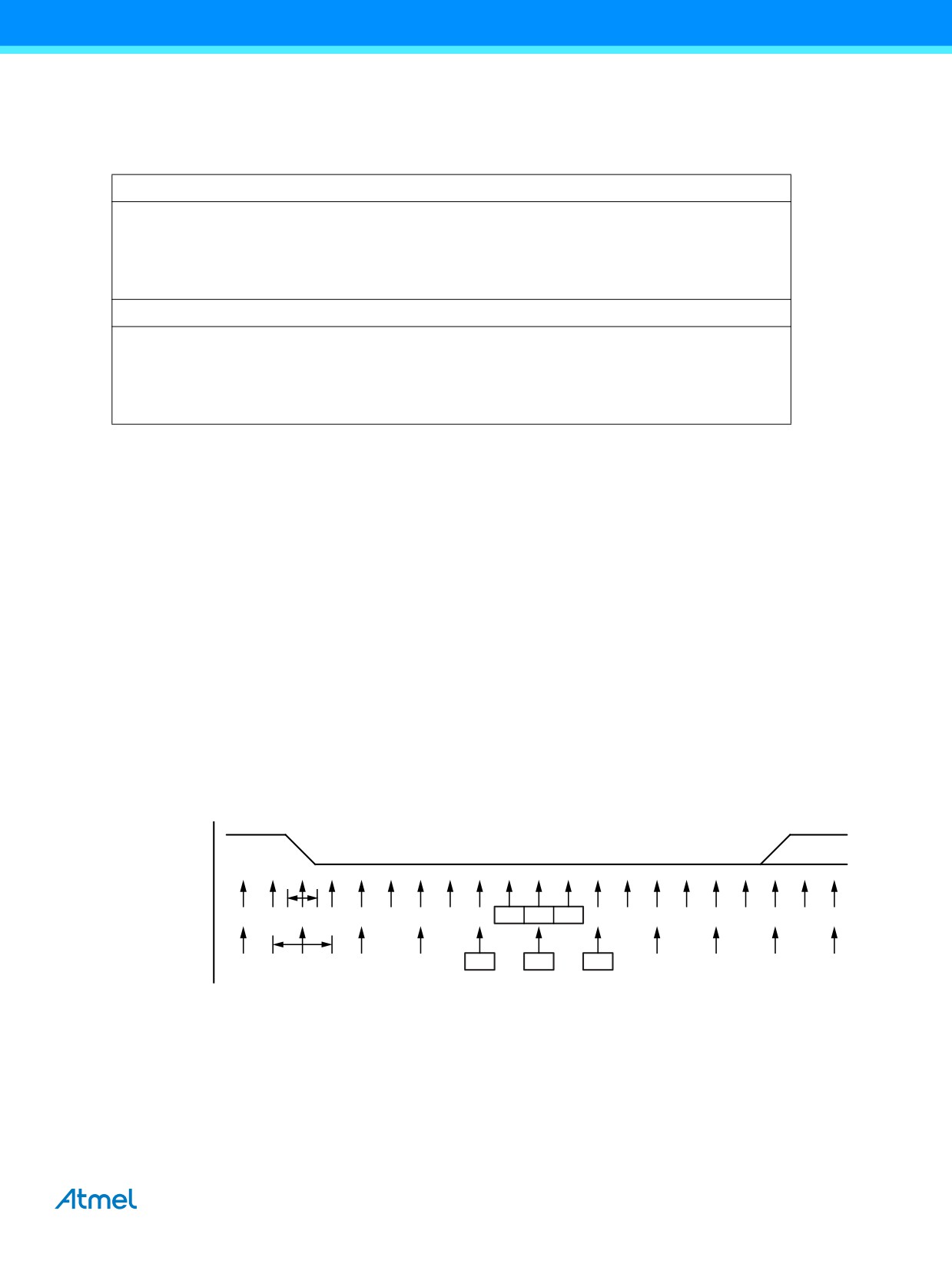
19.7.7
Flushing the Receive Buffer
The receiver buffer FIFO will be flushed when the receiver is disabled, i.e., the buffer will be emptied of its contents. Unread
data will be lost. If the buffer has to be flushed during normal operation, due to for instance an error condition, read the UDRn
I/O location until the RXCn flag is cleared. The following code example shows how to flush the receive buffer.
Assembly Code Example(1)
USART_Flush:
sbis UCSRnA, RXCn
ret
in
r16, UDRn
rjmp
USART_Flush
C Code Example(1)
void USART_Flush(void)
{
unsigned char dummy;
while (UCSRnA & (1<<RXCn)) dummy = UDRn;
}
Note:
1.
See Section 5. “About Code Examples” on page 8.
For I/O registers located in extended I/O map, “IN”, “OUT”, “SBIS”, “SBIC”, “CBI”, and “SBI” instructions must
be replaced with instructions that allow access to extended I/O. Typically “LDS” and “STS” combined with
“SBRS”, “SBRC”, “SBR”, and “CBR”.
19.8
Asynchronous Data Reception
The USART includes a clock recovery and a data recovery unit for handling asynchronous data reception. The clock
recovery logic is used for synchronizing the internally generated baud rate clock to the incoming asynchronous serial frames
at the RxDn pin. The data recovery logic samples and low pass filters each incoming bit, thereby improving the noise
immunity of the receiver. The asynchronous reception operational range depends on the accuracy of the internal baud rate
clock, the rate of the incoming frames, and the frame size in number of bits.
19.8.1
Asynchronous Clock Recovery
The clock recovery logic synchronizes internal clock to the incoming serial frames. Figure 19-5 illustrates the sampling
process of the start bit of an incoming frame. The sample rate is 16 times the baud rate for Normal mode, and eight times the
baud rate for double speed mode. The horizontal arrows illustrate the synchronization variation due to the sampling process.
Note the larger time variation when using the double speed mode (U2Xn = 1) of operation. Samples denoted zero are
samples done when the RxDn line is idle (i.e., no communication activity).
Figure 19-5. Start Bit Sampling
RxD
IDLE
START
BIT 0
Sample
(U2X = 0)
0
0
1
2
3
4
5
6
7
8
9
10
11
12
13
14
15
16
1
2
3
Sample
(U2X = 1)
0
1
2
3
4
5
6
7
8
1
2
When the clock recovery logic detects a high (idle) to low (start) transition on the RxDn line, the start bit detection sequence
is initiated. Let sample 1 denote the first zero-sample as shown in the figure. The clock recovery logic then uses samples 8,
9, and 10 for normal mode, and samples 4, 5, and 6 for double speed mode (indicated with sample numbers inside boxes on
the figure), to decide if a valid start bit is received. If two or more of these three samples have logical high levels (the majority
wins), the start bit is rejected as a noise spike and the receiver starts looking for the next high to low-transition. If however, a
valid start bit is detected, the clock recovery logic is synchronized and the data recovery can begin. The synchronization
process is repeated for each start bit.
ATmega328P [DATASHEET]
155
7810D-AVR-01/15
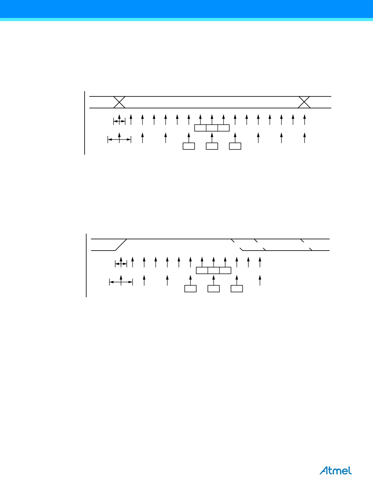
19.8.2
Asynchronous Data Recovery
When the receiver clock is synchronized to the start bit, the data recovery can begin. The data recovery unit uses a state
machine that has 16 states for each bit in normal mode and eight states for each bit in double speed mode. Figure 19-6
shows the sampling of the data bits and the parity bit. Each of the samples is given a number that is equal to the state of the
recovery unit.
Figure 19-6. Sampling of Data and Parity Bit
RxD
Bit n
Sample
(U2X = 0)
1
2
3
4
5
6
7
8
9
10
11
12
13
14
15
16
1
Sample
(U2X = 1)
1
2
3
4
5
6
7
8
1
The decision of the logic level of the received bit is taken by doing a majority voting of the logic value to the three samples in
the center of the received bit. The center samples are emphasized on the figure by having the sample number inside boxes.
The majority voting process is done as follows: If two or all three samples have high levels, the received bit is registered to
be a logic 1. If two or all three samples have low levels, the received bit is registered to be a logic 0. This majority voting
process acts as a low pass filter for the incoming signal on the RxDn pin. The recovery process is then repeated until a
complete frame is received. Including the first stop bit. Note that the receiver only uses the first stop bit of a frame.
Figure 19-7 shows the sampling of the stop bit and the earliest possible beginning of the start bit of the next frame.
Figure 19-7. Stop Bit Sampling and Next Start Bit Sampling
RxD
(A)
(B)
(C)
STOP 1
Sample
(U2X = 0)
1
2
3
4
5
6
7
8
9
10
0/1
0/1
0/1
Sample
(U2X = 1)
1
2
3
4
5
6
0/1
The same majority voting is done to the stop bit as done for the other bits in the frame. If the stop bit is registered to have a
logic 0 value, the frame error (FEn) flag will be set.
A new high to low transition indicating the start bit of a new frame can come right after the last of the bits used for majority
voting. For normal speed mode, the first low level sample can be at point marked (A) in Figure 19-7. For double speed mode
the first low level must be delayed to (B). (C) marks a stop bit of full length. The early start bit detection influences the
operational range of the receiver.
156
ATmega328P [DATASHEET]
7810D-AVR-01/15
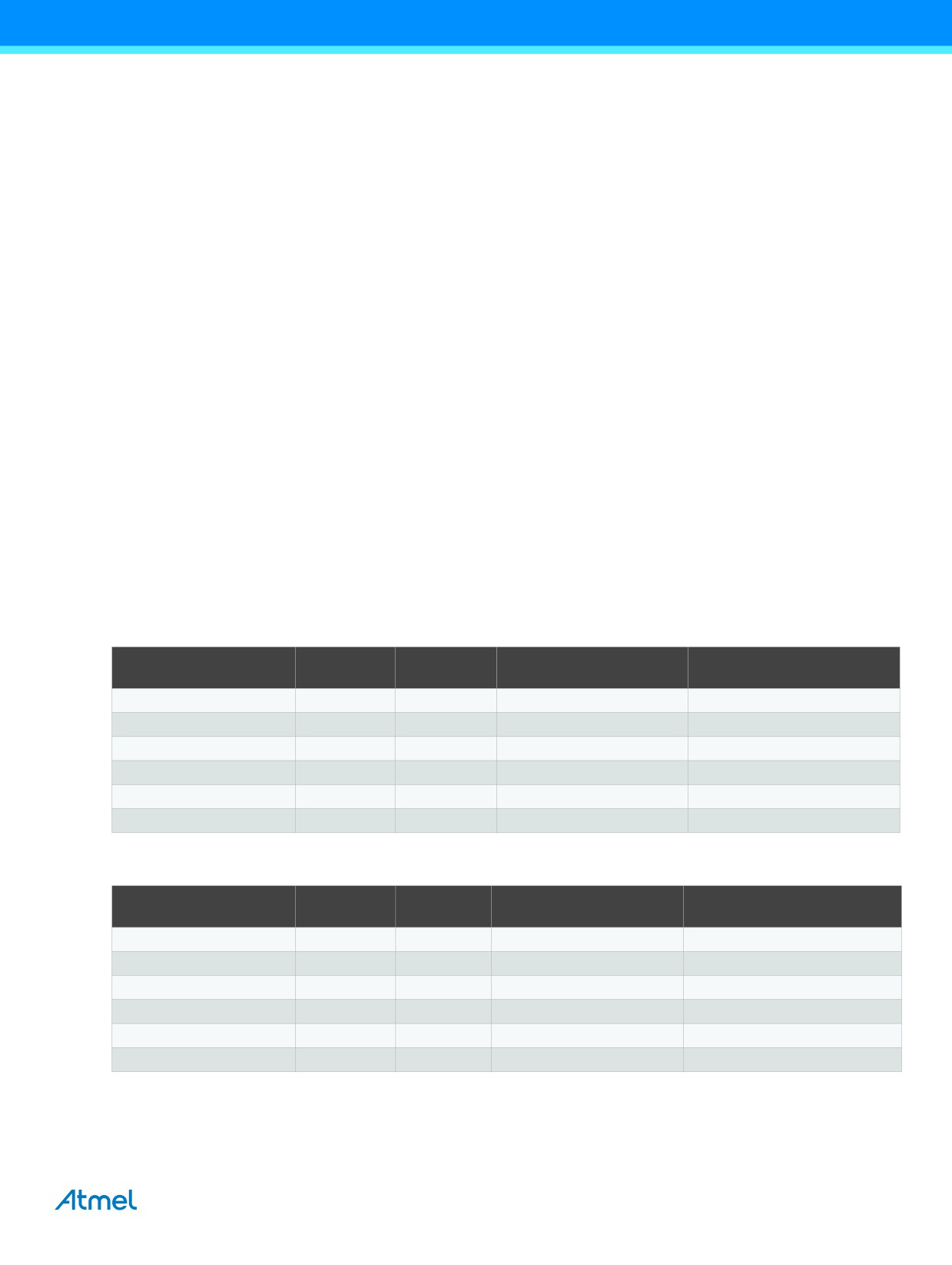
19.8.3
Asynchronous Operational Range
The operational range of the receiver is dependent on the mismatch between the received bit rate and the internally
generated baud rate. If the transmitter is sending frames at too fast or too slow bit rates, or the internally generated baud rate
of the receiver does not have a similar (see Table 19-2) base frequency, the receiver will not be able to synchronize the
frames to the start bit.
The following equations can be used to calculate the ratio of the incoming data rate and internal receiver baud rate.
Rfast
= -----------------------------------
Rslow
= --------------------------------------------
D+1S+ SM
S-1+DS+S
F
D
Sum of character size and parity size (D = 5 to 10 bit)
S
Samples per bit. S = 16 for normal speed mode and S = 8 for double speed
mode.
SF
First sample number used for majority voting. SF = 8 for normal speed and
SF = 4 for double speed mode.
SM
Middle sample number used for majority voting. SM = 9 for normal speed and
SM = 5 for double speed mode.
Rslow
is the ratio of the slowest incoming data rate that can be accepted in relation to
the receiver baud rate. Rfast is the ratio of the fastest incoming data rate that can
be accepted in relation to the receiver baud rate.
Table 19-2 and Table 19-3 list the maximum receiver baud rate error that can be tolerated. Note that normal speed mode has
higher toleration of baud rate variations.
Table 19-2. Recommended Maximum Receiver Baud Rate Error for Normal Speed Mode (U2Xn = 0)
D
Recommended Max Receiver
# (Data+Parity Bit)
Rslow (%)
Rfast (%)
Max Total Error (%)
Error (%)
5
93.20
106.67
+6.67/-6.8
±3.0
6
94.12
105.79
+5.79/-5.88
±2.5
7
94.81
105.11
+5.11/-5.19
±2.0
8
95.36
104.58
+4.58/-4.54
±2.0
9
95.81
104.14
+4.14/-4.19
±1.5
10
96.17
103.78
+3.78/-3.83
±1.5
Table 19-3. Recommended Maximum Receiver Baud Rate Error for Double Speed Mode (U2Xn = 1)
D
Recommended Max Receiver
# (Data+Parity Bit)
Rslow (%)
Rfast (%)
Max Total Error (%)
Error (%)
5
94.12
105.66
+5.66/-5.88
±2.5
6
94.92
104.92
+4.92/-5.08
±2.0
7
95.52
104,35
+4.35/-4.48
±1.5
8
96.00
103.90
+3.90/-4.00
±1.5
9
96.39
103.53
+3.53/-3.61
±1.5
10
96.70
103.23
+3.23/-3.30
±1.0
ATmega328P [DATASHEET]
157
7810D-AVR-01/15
The recommendations of the maximum receiver baud rate error was made under the assumption that the receiver and
transmitter equally divides the maximum total error.
There are two possible sources for the receivers baud rate error. The receiver’s system clock (XTAL) will always have some
minor instability over the supply voltage range and the temperature range. When using a crystal to generate the system
clock, this is rarely a problem, but for a resonator the system clock may differ more than 2% depending of the resonators
tolerance. The second source for the error is more controllable. The baud rate generator can not always do an exact division
of the system frequency to get the baud rate wanted. In this case an UBRRn value that gives an acceptable low error can be
used if possible.
19.9
Multi-processor Communication Mode
Setting the multi-processor communication mode (MPCMn) bit in UCSRnA enables a filtering function of incoming frames
received by the USART receiver. Frames that do not contain address information will be ignored and not put into the receive
buffer. This effectively reduces the number of incoming frames that has to be handled by the CPU, in a system with multiple
MCUs that communicate via the same serial bus. The transmitter is unaffected by the MPCMn setting, but has to be used
differently when it is a part of a system utilizing the multi-processor communication mode.
If the receiver is set up to receive frames that contain 5 to 8 data bits, then the first stop bit indicates if the frame contains
data or address information. If the receiver is set up for frames with nine data bits, then the ninth bit (RXB8n) is used for
identifying address and data frames. When the frame type bit (the first stop or the ninth bit) is one, the frame contains an
address. When the frame type bit is zero the frame is a data frame.
The multi-processor communication mode enables several slave MCUs to receive data from a master MCU. This is done by
first decoding an address frame to find out which MCU has been addressed. If a particular slave MCU has been addressed,
it will receive the following data frames as normal, while the other slave MCUs will ignore the received frames until another
address frame is received.
19.9.1
Using MPCMn
For an MCU to act as a master MCU, it can use a 9-bit character frame format (UCSZn = 7). The ninth bit (TXB8n) must be
set when an address frame (TXB8n = 1) or cleared when a data frame (TXB = 0) is being transmitted. The slave MCUs must
in this case be set to use a 9-bit character frame format.
The following procedure should be used to exchange data in multi-processor communication mode:
1.
All Slave MCUs are in multi-processor communication mode (MPCMn in
UCSRnA is set).
2.
The master MCU sends an address frame, and all slaves receive and read this frame. In the Slave MCUs, the
RXCn flag in UCSRnA will be set as normal.
3.
Each slave MCU reads the UDRn register and determines if it has been selected. If so, it clears the MPCMn bit in
UCSRnA, otherwise it waits for the next address byte and keeps the MPCMn setting.
4.
The addressed MCU will receive all data frames until a new address frame is received. The other slave MCUs,
which still have the MPCMn bit set, will ignore the data frames.
5.
When the last data frame is received by the addressed MCU, the addressed MCU sets the MPCMn bit and waits
for a new address frame from master. The process then repeats from 2.
Using any of the 5- to 8-bit character frame formats is possible, but impractical since the receiver must change between
using n and n+1 character frame formats. This makes full-duplex operation difficult since the transmitter and receiver uses
the same character size setting. If 5- to 8-bit character frames are used, the transmitter must be set to use two stop bit
(USBSn = 1) since the first stop bit is used for indicating the frame type.
Do not use read-modify-write instructions (SBI and CBI) to set or clear the MPCMn bit. The MPCMn bit shares the same I/O
location as the TXCn flag and this might accidentally be cleared when using SBI or CBI instructions.
158
ATmega328P [DATASHEET]
7810D-AVR-01/15
19.10
Register Description
19.10.1 UDRn - USART I/O Data Register n
Bit
7
6
5
4
3
2
1
0
RXB[7:0]
UDRn (Read)
TXB[7:0]
UDRn (Write)
Read/Write
R/W
R/W
R/W
R/W
R/W
R/W
R/W
R/W
Initial Value
0
0
0
0
0
0
0
0
The USART transmit data buffer register and USART receive data buffer registers share the same I/O address referred to as
USART data register or UDRn. The transmit data buffer register (TXB) will be the destination for data written to the UDRn
register location. Reading the UDRn register location will return the contents of the receive data buffer register (RXB).
For 5-, 6-, or 7-bit characters the upper unused bits will be ignored by the transmitter and set to zero by the receiver.
The transmit buffer can only be written when the UDREn flag in the UCSRnA register is set. Data written to UDRn when the
UDREn flag is not set, will be ignored by the USART transmitter. When data is written to the transmit buffer, and the
transmitter is enabled, the transmitter will load the data into the transmit shift register when the shift register is empty. Then
the data will be serially transmitted on the TxDn pin.
The receive buffer consists of a two level FIFO. The FIFO will change its state whenever the receive buffer is accessed. Due
to this behavior of the receive buffer, do not use read-modify-write instructions (SBI and CBI) on this location. Be careful
when using bit test instructions (SBIC and SBIS), since these also will change the state of the FIFO.
19.10.2 UCSRnA - USART Control and Status Register n A
Bit
7
6
5
4
3
2
1
0
RXCn
TXCn
UDREn
FEn
DORn
UPEn
U2Xn
MPCMn
UCSRnA
Read/Write
R
R/W
R
R
R
R
R/W
R/W
Initial Value
0
0
1
0
0
0
0
0
• Bit 7 - RXCn: USART Receive Complete
This flag bit is set when there are unread data in the receive buffer and cleared when the receive buffer is empty (i.e., does
not contain any unread data). If the receiver is disabled, the receive buffer will be flushed and consequently the RXCn bit will
become zero. The RXCn flag can be used to generate a receive complete interrupt (see description of the RXCIEn bit).
• Bit 6 - TXCn: USART Transmit Complete
This flag bit is set when the entire frame in the transmit shift register has been shifted out and there are no new data currently
present in the transmit buffer (UDRn). The TXCn flag bit is automatically cleared when a transmit complete interrupt is
executed, or it can be cleared by writing a one to its bit location. The TXCn flag can generate a transmit complete interrupt
(see description of the TXCIEn bit).
• Bit 5 - UDREn: USART Data Register Empty
The UDREn flag indicates if the transmit buffer (UDRn) is ready to receive new data. If UDREn is one, the buffer is empty,
and therefore ready to be written. The UDREn flag can generate a data register empty interrupt (see description of the
UDRIEn bit). UDREn is set after a reset to indicate that the transmitter is ready.
• Bit 4 - FEn: Frame Error
This bit is set if the next character in the receive buffer had a frame error when received. I.e., when the first stop bit of the
next character in the receive buffer is zero. This bit is valid until the receive buffer (UDRn) is read. The FEn bit is zero when
the stop bit of received data is one. Always set this bit to zero when writing to UCSRnA.
• Bit 3 - DORn: Data OverRun
This bit is set if a data overrun condition is detected. A data overrun occurs when the receive buffer is full (two characters), it
is a new character waiting in the receive shift register, and a new start bit is detected. This bit is valid until the receive buffer
(UDRn) is read. Always set this bit to zero when writing to UCSRnA.
ATmega328P [DATASHEET]
159
7810D-AVR-01/15