Atmel ATmega328P 8-bit AVR Microcontroller. DATASHEET (2015) - page 5
• Bit 2 - UPEn: USART Parity Error
This bit is set if the next character in the receive buffer had a parity error when received and the parity checking was enabled
at that point (UPMn1 = 1). This bit is valid until the receive buffer (UDRn) is read. Always set this bit to zero when writing to
UCSRnA.
• Bit 1 - U2Xn: Double the USART Transmission Speed
This bit only has effect for the asynchronous operation. Write this bit to zero when using synchronous operation.
Writing this bit to one will reduce the divisor of the baud rate divider from 16 to 8 effectively doubling the transfer rate for
asynchronous communication.
• Bit 0 - MPCMn: Multi-processor Communication Mode
This bit enables the multi-processor communication mode. When the MPCMn bit is written to one, all the incoming frames
received by the USART receiver that do not contain address information will be ignored. The transmitter is unaffected by the
MPCMn setting. For more detailed information see Section 19.9 “Multi-processor Communication Mode” on page 158.
19.10.3 UCSRnB - USART Control and Status Register n B
Bit
7
6
5
4
3
2
1
0
RXCIEn
TXCIEn
UDRIEn
RXENn
TXENn
UCSZn2
RXB8n
TXB8n
UCSRnB
Read/Write
R/W
R/W
R/W
R/W
R/W
R/W
R
R/W
Initial Value
0
0
0
0
0
0
0
0
• Bit 7 - RXCIEn: RX Complete Interrupt Enable n
Writing this bit to one enables interrupt on the RXCn flag. A USART receive complete interrupt will be generated only if the
RXCIEn bit is written to one, the global interrupt flag in SREG is written to one and the RXCn bit in UCSRnA is set.
• Bit 6 - TXCIEn: TX Complete Interrupt Enable n
Writing this bit to one enables interrupt on the TXCn flag. A USART transmit complete interrupt will be generated only if the
TXCIEn bit is written to one, the global interrupt flag in SREG is written to one and the TXCn bit in UCSRnA is set.
• Bit 5 - UDRIEn: USART Data Register Empty Interrupt Enable n
Writing this bit to one enables interrupt on the UDREn flag. A data register empty interrupt will be generated only if the
UDRIEn bit is written to one, the global interrupt flag in SREG is written to one and the UDREn bit in UCSRnA is set.
• Bit 4 - RXENn: Receiver Enable n
Writing this bit to one enables the USART receiver. The receiver will override normal port operation for the RxDn pin when
enabled. Disabling the receiver will flush the receive buffer invalidating the FEn, DORn, and UPEn flags.
• Bit 3 - TXENn: Transmitter Enable n
Writing this bit to one enables the USART transmitter. The transmitter will override normal port operation for the TxDn pin
when enabled. The disabling of the transmitter (writing TXENn to zero) will not become effective until ongoing and pending
transmissions are completed, i.e., when the transmit shift register and transmit buffer register do not contain data to be
transmitted. When disabled, the transmitter will no longer override the TxDn port.
• Bit 2 - UCSZn2: Character Size n
The UCSZn2 bits combined with the UCSZn1:0 bit in UCSRnC sets the number of data bits (character size) in a frame the
receiver and transmitter use.
• Bit 1 - RXB8n: Receive Data Bit 8 n
RXB8n is the ninth data bit of the received character when operating with serial frames with nine data bits. Must be read
before reading the low bits from UDRn.
• Bit 0 - TXB8n: Transmit Data Bit 8 n
TXB8n is the ninth data bit in the character to be transmitted when operating with serial frames with nine data bits. Must be
written before writing the low bits to UDRn.
160
ATmega328P [DATASHEET]
7810D-AVR-01/15
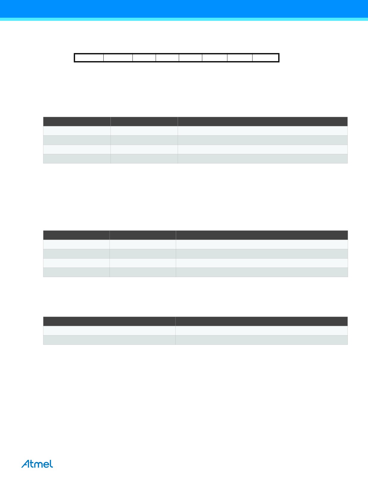
19.10.4 UCSRnC - USART Control and Status Register n C
Bit
7
6
5
4
3
2
1
0
UMSELn1
UMSELn0
UPMn1
UPMn0
USBSn
UCSZn1
UCSZn0
UCPOLn
UCSRnC
Read/Write
R/W
R/W
R/W
R/W
R/W
R/W
R/W
R/W
Initial Value
0
0
0
0
0
1
1
0
• Bits 7:6 - UMSELn1:0 USART Mode Select
These bits select the mode of operation of the USARTn as shown in Table 19-4.
Table 19-4. UMSELn Bits Settings
UMSELn1
UMSELn0
Mode
0
0
Asynchronous USART
0
1
Synchronous USART
1
0
(Reserved)
1
1
Master SPI (MSPIM)(1)
Note:
1.
See Section 20. “USART in SPI Mode” on page 166 for full description of the master SPI mode (MSPIM)
operation
• Bits 5:4 - UPMn1:0: Parity Mode
These bits enable and set type of parity generation and check. If enabled, the transmitter will automatically generate and
send the parity of the transmitted data bits within each frame. The receiver will generate a parity value for the incoming data
and compare it to the UPMn setting. If a mismatch is detected, the UPEn flag in UCSRnA will be set.
Table 19-5. UPMn Bits Settings
UPMn1
UPMn0
Parity Mode
0
0
Disabled
0
1
Reserved
1
0
Enabled, even parity
1
1
Enabled, odd parity
• Bit 3 - USBSn: Stop Bit Select
This bit selects the number of stop bits to be inserted by the transmitter. The receiver ignores this setting.
Table 19-6. USBS Bit Settings
USBSn
Stop Bit(s)
0
1-bit
1
2-bit
ATmega328P [DATASHEET]
161
7810D-AVR-01/15
• Bit 2:1 - UCSZn1:0: Character Size
The UCSZn1:0 bits combined with the UCSZn2 bit in UCSRnB sets the number of data bits (character size) in a frame the
receiver and transmitter use.
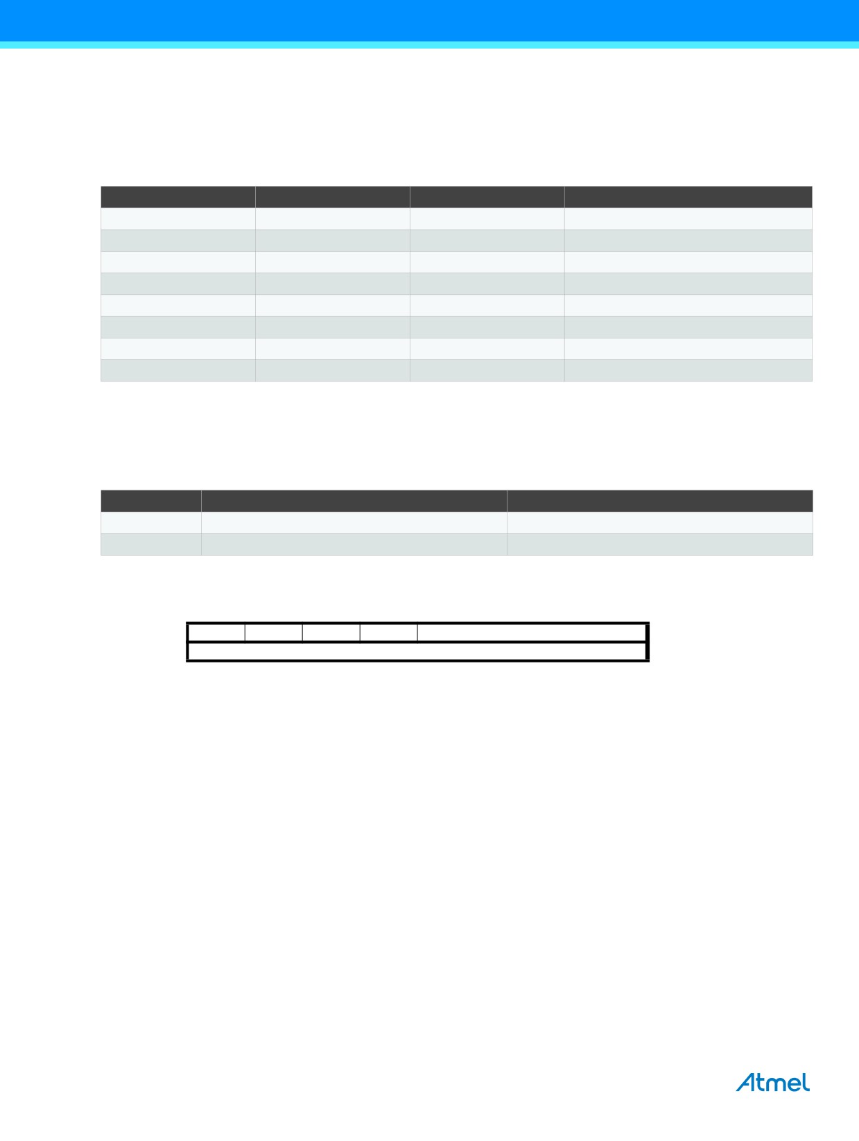
Table 19-7. UCSZn Bits Settings
UCSZn2
UCSZn1
UCSZn0
Character Size
0
0
0
5-bit
0
0
1
6-bit
0
1
0
7-bit
0
1
1
8-bit
1
0
0
Reserved
1
0
1
Reserved
1
1
0
Reserved
1
1
1
9-bit
• Bit 0 - UCPOLn: Clock Polarity
This bit is used for synchronous mode only. Write this bit to zero when asynchronous mode is used. The UCPOLn bit sets
the relationship between data output change and data input sample, and the synchronous clock (XCKn).
Table 19-8. UCPOLn Bit Settings
UCPOLn
Transmitted Data Changed (Output of TxDn Pin)
Received Data Sampled (Input on RxDn Pin)
0
Rising XCKn edge
Falling XCKn edge
1
Falling XCKn edge
Rising XCKn edge
19.10.5 UBRRnL and UBRRnH - USART Baud Rate Registers
Bit
15
14
13
12
11
10
9
8
–
-
-
-
UBRRn[11:8]
UBRRnH
UBRRn[7:0]
UBRRnL
7
6
5
4
3
2
1
0
R
R
R
R
R/W
R/W
R/W
R/W
Read/Write
R/W
R/W
R/W
R/W
R/W
R/W
R/W
R/W
0
0
0
0
0
0
0
0
Initial Value
0
0
0
0
0
0
0
0
• Bit 15:12 - Reserved Bits
These bits are reserved for future use. For compatibility with future devices, these bit must be written to zero when UBRRnH
is written.
• Bit 11:0 - UBRR11:0: USART Baud Rate Register
This is a 12-bit register which contains the USART baud rate. The UBRRnH contains the four most significant bits, and the
UBRRnL contains the eight least significant bits of the USART baud rate. Ongoing transmissions by the transmitter and
receiver will be corrupted if the baud rate is changed. Writing UBRRnL will trigger an immediate update of the baud rate
prescaler.
162
ATmega328P [DATASHEET]
7810D-AVR-01/15
19.11
Examples of Baud Rate Setting
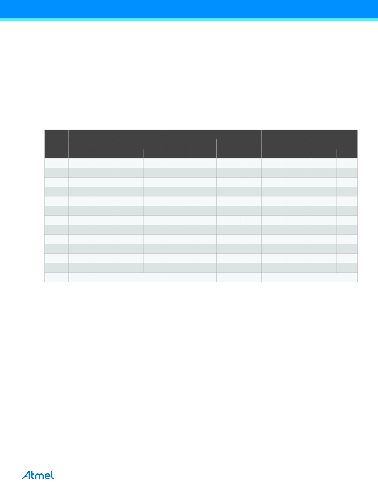
For standard crystal and resonator frequencies, the most commonly used baud rates for asynchronous operation can be
generated by using the UBRRn settings in Table 19-9. UBRRn values which yield an actual baud rate differing less than
0.5% from the target baud rate, are bold in the table. Higher error ratings are acceptable, but the receiver will have less noise
resistance when the error ratings are high, especially for large serial frames (see Section 19.8.3 “Asynchronous Operational
Range” on page 157). The error values are calculated using the following equation:
BaudRateClosest Match
Error%
=
-------------------------------------------------- - 1
100%
BaudRate
Table 19-9. Examples of UBRRn Settings for Commonly Used Oscillator Frequencies
fosc = 1.0000MHz
fosc = 1.8432MHz
fosc
= 2.0000MHz
Baud
U2Xn = 0
U2Xn = 1
U2Xn = 0
U2Xn = 1
U2Xn = 0
U2Xn = 1
Rate
(bps)
UBRRn
Error
UBRRn
Error
UBRRn
Error
UBRRn
Error
UBRRn
Error
UBRRn
Error
2400
25
0.2%
51
0.2%
47
0.0%
95
0.0%
51
0.2%
103
0.2%
4800
12
0.2%
25
0.2%
23
0.0%
47
0.0%
25
0.2%
51
0.2%
9600
6
-7.0%
12
0.2%
11
0.0%
23
0.0%
12
0.2%
25
0.2%
14.4k
3
8.5%
8
-3.5%
7
0.0%
15
0.0%
8
-3.5%
16
2.1%
19.2k
2
8.5%
6
-7.0%
5
0.0%
11
0.0%
6
-7.0%
12
0.2%
28.8k
1
8.5%
3
8.5%
3
0.0%
7
0.0%
3
8.5%
8
-3.5%
38.4k
1
-18.6%
2
8.5%
2
0.0%
5
0.0%
2
8.5%
6
-7.0%
57.6k
0
8.5%
1
8.5%
1
0.0%
3
0.0%
1
8.5%
3
8.5%
76.8k
-
-
1
-18.6%
1
-25.0%
2
0.0%
1
-18.6%
2
8.5%
115.2k
-
-
0
8.5%
0
0.0%
1
0.0%
0
8.5%
1
8.5%
230.4k
-
-
-
-
-
-
0
0.0%
-
-
-
-
250k
-
-
-
-
-
-
-
-
-
-
0
0.0%
Max.(1)
62.5kbps
125kbps
115.2kbps
230.4kbps
125kbps
250kbps
Note:
1.
UBRRn = 0, error = 0.0%
ATmega328P [DATASHEET]
163
7810D-AVR-01/15

Table 19-10. Examples of UBRRn Settings for Commonly Used Oscillator Frequencies
fosc = 3.6864MHz
fosc = 4.0000MHz
fosc
= 7.3728MHz
Baud
U2Xn = 0
U2Xn = 1
U2Xn = 0
U2Xn = 1
U2Xn = 0
U2Xn = 1
Rate
(bps)
UBRRn
Error
UBRRn
Error
UBRRn
Error
UBRRn
Error
UBRRn
Error
UBRRn
Error
2400
95
0.0%
191
0.0%
103
0.2%
207
0.2%
191
0.0%
383
0.0%
4800
47
0.0%
95
0.0%
51
0.2%
103
0.2%
95
0.0%
191
0.0%
9600
23
0.0%
47
0.0%
25
0.2%
51
0.2%
47
0.0%
95
0.0%
14.4k
15
0.0%
31
0.0%
16
2.1%
34
-0.8%
31
0.0%
63
0.0%
19.2k
11
0.0%
23
0.0%
12
0.2%
25
0.2%
23
0.0%
47
0.0%
28.8k
7
0.0%
15
0.0%
8
-3.5%
16
2.1%
15
0.0%
31
0.0%
38.4k
5
0.0%
11
0.0%
6
-7.0%
12
0.2%
11
0.0%
23
0.0%
57.6k
3
0.0%
7
0.0%
3
8.5%
8
-3.5%
7
0.0%
15
0.0%
76.8k
2
0.0%
5
0.0%
2
8.5%
6
-7.0%
5
0.0%
11
0.0%
115.2k
1
0.0%
3
0.0%
1
8.5%
3
8.5%
3
0.0%
7
0.0%
230.4k
0
0.0%
1
0.0%
0
8.5%
1
8.5%
1
0.0%
3
0.0%
250k
0
-7.8%
1
-7.8%
0
0.0%
1
0.0%
1
-7.8%
3
-7.8%
0.5M
-
-
0
-7.8%
-
-
0
0.0%
0
-7.8%
1
-7.8%
1M
-
-
-
-
-
-
-
-
-
-
0
-7.8%
Max.(1)
230.4kbps
460.8kbps
250kbps
0.5Mbps
460.8kbps
921.6kbps
Note:
1.
UBRRn = 0, error = 0.0%
Table 19-11. Examples of UBRRn Settings for Commonly Used Oscillator Frequencies
fosc = 8.0000MHz
fosc = 11.0592MHz
fosc
= 14.7456MHz
Baud
U2Xn = 0
U2Xn = 1
U2Xn = 0
U2Xn = 1
U2Xn = 0
U2Xn = 1
Rate
(bps)
UBRRn
Error
UBRRn
Error
UBRRn
Error
UBRRn
Error
UBRRn
Error
UBRRn
Error
2400
207
0.2%
416
-0.1%
287
0.0%
575
0.0%
383
0.0%
767
0.0%
4800
103
0.2%
207
0.2%
143
0.0%
287
0.0%
191
0.0%
383
0.0%
9600
51
0.2%
103
0.2%
71
0.0%
143
0.0%
95
0.0%
191
0.0%
14.4k
34
-0.8%
68
0.6%
47
0.0%
95
0.0%
63
0.0%
127
0.0%
19.2k
25
0.2%
51
0.2%
35
0.0%
71
0.0%
47
0.0%
95
0.0%
28.8k
16
2.1%
34
-0.8%
23
0.0%
47
0.0%
31
0.0%
63
0.0%
38.4k
12
0.2%
25
0.2%
17
0.0%
35
0.0%
23
0.0%
47
0.0%
57.6k
8
-3.5%
16
2.1%
11
0.0%
23
0.0%
15
0.0%
31
0.0%
76.8k
6
-7.0%
12
0.2%
8
0.0%
17
0.0%
11
0.0%
23
0.0%
115.2k
3
8.5%
8
-3.5%
5
0.0%
11
0.0%
7
0.0%
15
0.0%
230.4k
1
8.5%
3
8.5%
2
0.0%
5
0.0%
3
0.0%
7
0.0%
250k
1
0.0%
3
0.0%
2
-7.8%
5
-7.8%
3
-7.8%
6
5.3%
0.5M
0
0.0%
1
0.0%
-
-
2
-7.8%
1
-7.8%
3
-7.8%
1M
-
-
0
0.0%
-
-
-
-
0
-7.8%
1
-7.8%
Max.(1)
0.5Mbps
1Mbps
691.2kbps
1.3824Mbps
921.6kbps
1.8432Mbps
Note:
1.
UBRRn = 0, error = 0.0%
164
ATmega328P [DATASHEET]
7810D-AVR-01/15

Table 19-12. Examples of UBRRn Settings for Commonly Used Oscillator Frequencies
fosc = 16.0000MHz
U2Xn = 0
U2Xn = 1
Baud Rate (bps)
UBRRn
Error
UBRRn
Error
2400
416
-0.1%
832
0.0%
4800
207
0.2%
416
-0.1%
9600
103
0.2%
207
0.2%
14.4k
68
0.6%
138
-0.1%
19.2k
51
0.2%
103
0.2%
28.8k
34
-0.8%
68
0.6%
38.4k
25
0.2%
51
0.2%
57.6k
16
2.1%
34
-0.8%
76.8k
12
0.2%
25
0.2%
115.2k
8
-3.5%
16
2.1%
230.4k
3
8.5%
8
-3.5%
250k
3
0.0%
7
0.0%
0.5M
1
0.0%
3
0.0%
1M
0
0.0%
1
0.0%
Max.(1)
1Mbps
2Mbps
Note:
1.
UBRRn = 0, error = 0.0%
ATmega328P [DATASHEET]
165
7810D-AVR-01/15
20.
USART in SPI Mode
20.1
Features
● Full duplex, three-wire synchronous data transfer
● Master operation
● Supports all four SPI modes of operation (mode 0, 1, 2, and 3)
● LSB first or MSB first data transfer (configurable data order)
● Queued operation (double buffered)
● High resolution baud rate generator
● High speed operation (fXCKmax = fCK/2)
● Flexible interrupt generation
20.2
Overview
The universal synchronous and asynchronous serial receiver and transmitter (USART) can be set to a master SPI compliant
mode of operation.
Setting both UMSELn1:0 bits to one enables the USART in MSPIM logic. In this mode of operation the SPI master control
logic takes direct control over the USART resources. These resources include the transmitter and receiver shift register and
buffers, and the baud rate generator. The parity generator and checker, the data and clock recovery logic, and the RX and
TX control logic is disabled. The USART RX and TX control logic is replaced by a common SPI transfer control logic.
However, the pin control logic and interrupt generation logic is identical in both modes of operation.
The I/O register locations are the same in both modes. However, some of the functionality of the control registers changes
when using MSPIM.
20.3
Clock Generation
The clock generation logic generates the base clock for the transmitter and receiver. For USART MSPIM mode of operation
only internal clock generation (i.e. master operation) is supported. The data direction register for the XCKn pin (DDR_XCKn)
must therefore be set to one (i.e. as output) for the USART in MSPIM to operate correctly. Preferably the DDR_XCKn should
be set up before the USART in MSPIM is enabled (i.e. TXENn and RXENn bit set to one).
The internal clock generation used in MSPIM mode is identical to the USART synchronous master mode. The baud rate or
UBRRn setting can therefore be calculated using the same equations, see Table 20-1:
Table 20-1. Equations for Calculating Baud Rate Register Setting
Operating Mode
Equation for Calculating Baud Rate(1)
Equation for Calculating UBRRn Value
fOSC
fOSC
Synchronous master mode
BAUD
= ------------------------------------
UBRRn
= ------------------- - 1
2UBRRn + 1
2BAUD
Note:
1.
The baud rate is defined to be the transfer rate in bit per second (bps)
BAUD
Baud rate (in bits per second, bps)
fOSC
System oscillator clock frequency
UBRRn
Contents of the UBRRnH and UBRRnL registers, (0-4095)
166
ATmega328P [DATASHEET]
7810D-AVR-01/15
20.4
SPI Data Modes and Timing
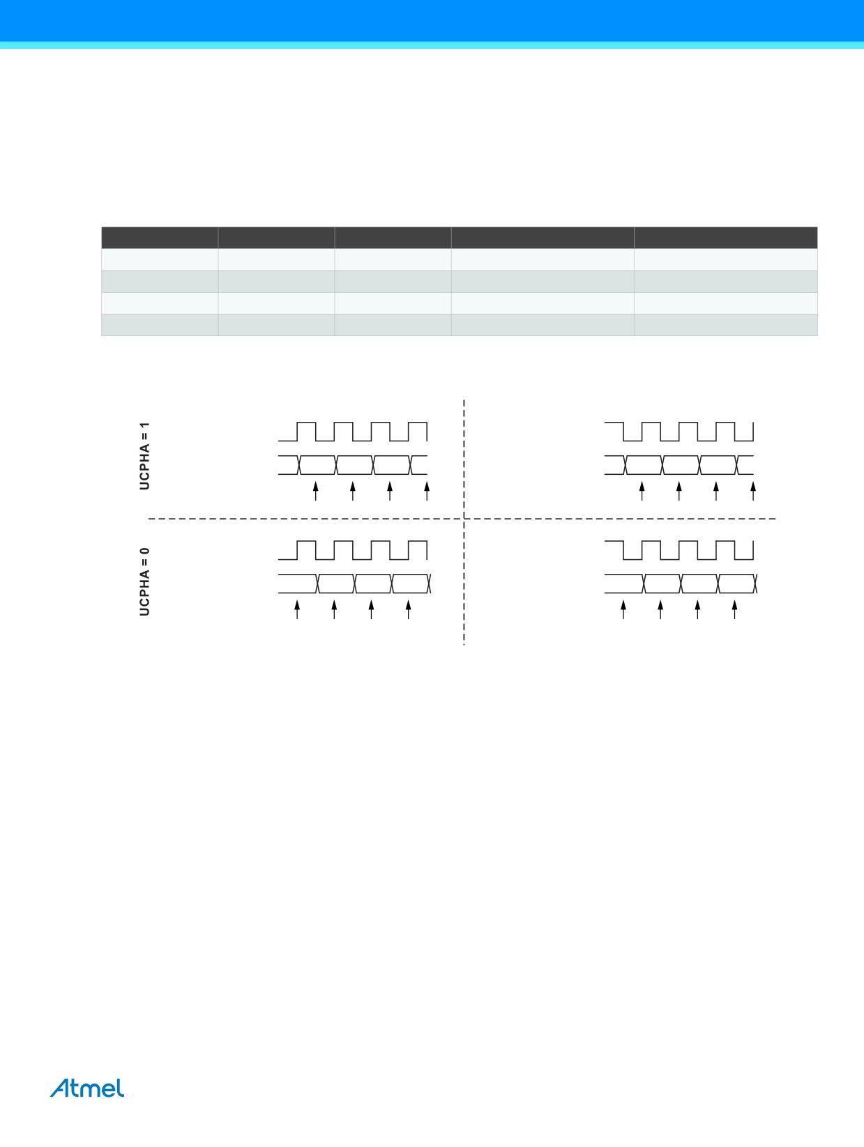
There are four combinations of XCKn (SCK) phase and polarity with respect to serial data, which are determined by control
bits UCPHAn and UCPOLn. The data transfer timing diagrams are shown in Figure 20-1. Data bits are shifted out and
latched in on opposite edges of the XCKn signal, ensuring sufficient time for data signals to stabilize. The UCPOLn and
UCPHAn functionality is summarized in Table 20-2. Note that changing the setting of any of these bits will corrupt all ongoing
communication for both the receiver and transmitter.
Table 20-2. UCPOLn and UCPHAn Functionality
UCPOLn
UCPHAn
SPI Mode
Leading Edge
Trailing Edge
0
0
0
Sample (rising)
Setup (falling)
0
1
1
Setup (rising)
Sample (falling)
1
0
2
Sample (falling)
Setup (rising)
1
1
3
Setup (falling)
Sample (rising)
Figure 20-1. UCPHAn and UCPOLn Data Transfer Timing Diagrams.
UCPOL = 0
UCPOL = 1
XCK
XCK
Data setup (TXD)
Data setup (TXD)
Data sample (RXD)
Data sample (RXD)
XCK
XCK
Data setup (TXD)
Data setup (TXD)
Data sample (RXD)
Data sample (RXD)
20.5
Frame Formats
A serial frame for the MSPIM is defined to be one character of 8 data bits. The USART in MSPIM mode has two valid frame
formats:
●
8-bit data with MSB first
●
8-bit data with LSB first
A frame starts with the least or most significant data bit. Then the next data bits, up to a total of eight, are succeeding, ending
with the most or least significant bit accordingly. When a complete frame is transmitted, a new frame can directly follow it, or
the communication line can be set to an idle (high) state.
The UDORDn bit in UCSRnC sets the frame format used by the USART in MSPIM mode. The receiver and transmitter use
the same setting. Note that changing the setting of any of these bits will corrupt all ongoing communication for both the
receiver and transmitter.
16-bit data transfer can be achieved by writing two data bytes to UDRn. A UART transmit complete interrupt will then signal
that the 16-bit value has been shifted out.
ATmega328P [DATASHEET]
167
7810D-AVR-01/15
20.5.1
USART MSPIM Initialization
The USART in MSPIM mode has to be initialized before any communication can take place. The initialization process
normally consists of setting the baud rate, setting master mode of operation (by setting DDR_XCKn to one), setting frame
format and enabling the transmitter and the receiver. Only the transmitter can operate independently. For interrupt driven
USART operation, the global interrupt flag should be cleared (and thus interrupts globally disabled) when doing the
initialization.
Note:
To ensure immediate initialization of the XCKn output the baud-rate register (UBRRn) must be zero at the time
the transmitter is enabled. Contrary to the normal mode USART operation the UBRRn must then be written to
the desired value after the transmitter is enabled, but before the first transmission is started. Setting UBRRn to
zero before enabling the transmitter is not necessary if the initialization is done immediately after a reset since
UBRRn is reset to zero.
Before doing a re-initialization with changed baud rate, data mode, or frame format, be sure that there is no ongoing
transmissions during the period the registers are changed. The TXCn flag can be used to check that the transmitter has
completed all transfers, and the RXCn flag can be used to check that there are no unread data in the receive buffer. Note
that the TXCn flag must be cleared before each transmission (before UDRn is written) if it is used for this purpose.
The following simple USART initialization code examples show one assembly and one C function that are equal in
functionality. The examples assume polling (no interrupts enabled). The baud rate is given as a function parameter. For the
assembly code, the baud rate parameter is assumed to be stored in the r17:r16 registers.
Assembly Code Example(1)
USART_Init:
clr r18
out UBRRnH,r18
out UBRRnL,r18
; Setting the XCKn port pin as output, enables master mode.
sbi XCKn_DDR, XCKn
; Set MSPI mode of operation and SPI data mode 0.
ldi r18, (1<<UMSELn1)|(1<<UMSELn0)|(0<<UCPHAn)|(0<<UCPOLn)
out UCSRnC,r18
; Enable receiver and transmitter.
ldi r18, (1<<RXENn)|(1<<TXENn)
out UCSRnB,r18
; Set baud rate.
; IMPORTANT: The Baud Rate must be set after the transmitter is
enabled!
out UBRRnH, r17
out UBRRnL, r18
ret
C Code Example(1)
void USART_Init(unsigned int baud)
{
UBRRn = 0;
/* Setting the XCKn port pin as output, enables master mode. */
XCKn_DDR |= (1<<XCKn);
/* Set MSPI mode of operation and SPI data mode 0. */
UCSRnC = (1<<UMSELn1)|(1<<UMSELn0)|(0<<UCPHAn)|(0<<UCPOLn);
/* Enable receiver and transmitter. */
UCSRnB = (1<<RXENn)|(1<<TXENn);
/* Set baud rate. */
/* IMPORTANT: The Baud Rate must be set after the transmitter is
enabled
*/
UBRRn = baud;
}
Note:
1.
See Section 5. “About Code Examples” on page 8.
168
ATmega328P [DATASHEET]
7810D-AVR-01/15
20.6
Data Transfer
Using the USART in MSPI mode requires the transmitter to be enabled, i.e. the TXENn bit in the UCSRnB register is set to
one. When the transmitter is enabled, the normal port operation of the TxDn pin is overridden and given the function as the
transmitter's serial output. Enabling the receiver is optional and is done by setting the RXENn bit in the UCSRnB register to
one. When the receiver is enabled, the normal pin operation of the RxDn pin is overridden and given the function as the
receiver's serial input. The XCKn will in both cases be used as the transfer clock.
After initialization the USART is ready for doing data transfers. A data transfer is initiated by writing to the UDRn I/O location.
This is the case for both sending and receiving data since the transmitter controls the transfer clock. The data written to
UDRn is moved from the transmit buffer to the shift register when the shift register is ready to send a new frame.
Note:
To keep the input buffer in sync with the number of data bytes transmitted, the UDRn register must be read
once for each byte transmitted. The input buffer operation is identical to normal USART mode, i.e. if an
overflow occurs the character last received will be lost, not the first data in the buffer. This means that if four
bytes are transferred, byte 1 first, then byte 2, 3, and 4, and the UDRn is not read before all transfers are
completed, then byte 3 to be received will be lost, and not byte 1.
The following code examples show a simple USART in MSPIM mode transfer function based on polling of the data register
empty (UDREn) flag and the receive complete (RXCn) Flag. The USART has to be initialized before the function can be
used. For the assembly code, the data to be sent is assumed to be stored in register R16 and the data received will be
available in the same register (R16) after the function returns.
The function simply waits for the transmit buffer to be empty by checking the UDREn flag, before loading it with new data to
be transmitted. The function then waits for data to be present in the receive buffer by checking the RXCn flag, before reading
the buffer and returning the value.
Assembly Code Example(1)
USART_MSPIM_Transfer:
; Wait for empty transmit buffer
sbis UCSRnA, UDREn
rjmp USART_MSPIM_Transfer
; Put data (r16) into buffer, sends the data
out UDRn,r16
; Wait for data to be received
USART_MSPIM_Wait_RXCn:
sbis UCSRnA, RXCn
rjmp USART_MSPIM_Wait_RXCn
; Get and return received data from buffer
in r16, UDRn
ret
C Code Example(1)
unsigned char USART_Receive(void)
{
/* Wait for empty transmit buffer */
while (!(UCSRnA & (1<<UDREn)));
/* Put data into buffer, sends the data */
UDRn = data;
/* Wait for data to be received */
while (!(UCSRnA & (1<<RXCn)));
/* Get and return received data from buffer */
return UDRn;
}
Note:
1.
See Section 5. “About Code Examples” on page 8.
ATmega328P [DATASHEET]
169
7810D-AVR-01/15

20.6.1
Transmitter and Receiver Flags and Interrupts
The RXCn, TXCn, and UDREn flags and corresponding interrupts in USART in MSPIM mode are identical in function to the
normal USART operation. However, the receiver error status flags (FE, DOR, and PE) are not in use and is always read as
zero.
20.6.2
Disabling the Transmitter or Receiver
The disabling of the transmitter or receiver in USART in MSPIM mode is identical in function to the normal USART operation.
20.7
AVR USART MSPIM versus AVR SPI
The USART in MSPIM mode is fully compatible with the AVR SPI regarding:
● Master mode timing diagram.
● The UCPOLn bit functionality is identical to the SPI CPOL bit.
● The UCPHAn bit functionality is identical to the SPI CPHA bit.
● The UDORDn bit functionality is identical to the SPI DORD bit.
However, since the USART in MSPIM mode reuses the USART resources, the use of the USART in MSPIM mode is
somewhat different compared to the SPI. In addition to differences of the control register bits, and that only master operation
is supported by the USART in MSPIM mode, the following features differ between the two modules:
● The USART in MSPIM mode includes (double) buffering of the transmitter. The SPI has no buffer.
● The USART in MSPIM mode receiver includes an additional buffer level.
● The SPI WCOL (write collision) bit is not included in USART in MSPIM mode.
● The SPI double speed mode (SPI2X) bit is not included. However, the same effect is achieved by setting UBRRn
accordingly.
● Interrupt timing is not compatible.
● Pin control differs due to the master only operation of the USART in MSPIM mode.
A comparison of the USART in MSPIM mode and the SPI pins is shown in Table 20-3.
Table 20-3. Comparison of USART in MSPIM Mode and SPI Pins
USART_MSPIM
SPI
Comment
TxDn
MOSI
Master out only
RxDn
MISO
Master in only
XCKn
SCK
(Functionally identical)
(N/A)
SS
Not supported by USART in MSPIM
20.8
Register Description
The following section describes the registers used for SPI operation using the USART.
20.8.1
UDRn - USART MSPIM I/O Data Register
The function and bit description of the USART data register (UDRn) in MSPI mode is identical to normal USART operation.
See Section 19.10.1 “UDRn - USART I/O Data Register n” on page 159.
20.8.2
UCSRnA - USART MSPIM Control and Status Register n A
Bit
7
6
5
4
3
2
1
0
RXCn
TXCn
UDREn
-
-
-
-
-
UCSRnA
Read/Write
R
R/W
R
R
R
R
R
R
Initial Value
0
0
0
0
0
1
1
0
170
ATmega328P [DATASHEET]
7810D-AVR-01/15
• Bit 7 - RXCn: USART Receive Complete
This flag bit is set when there are unread data in the receive buffer and cleared when the receive buffer is empty (i.e., does
not contain any unread data). If the receiver is disabled, the receive buffer will be flushed and consequently the RXCn bit will
become zero. The RXCn flag can be used to generate a receive complete interrupt (see description of the RXCIEn bit).
• Bit 6 - TXCn: USART Transmit Complete
This flag bit is set when the entire frame in the transmit shift register has been shifted out and there are no new data currently
present in the transmit buffer (UDRn). The TXCn flag bit is automatically cleared when a transmit complete interrupt is
executed, or it can be cleared by writing a one to its bit location. The TXCn flag can generate a transmit complete interrupt
(see description of the TXCIEn bit).
• Bit 5 - UDREn: USART Data Register Empty
The UDREn flag indicates if the transmit buffer (UDRn) is ready to receive new data. If UDREn is one, the buffer is empty,
and therefore ready to be written. The UDREn flag can generate a data register empty interrupt (see description of the
UDRIE bit). UDREn is set after a reset to indicate that the transmitter is ready.
• Bit 4:0 - Reserved Bits in MSPI mode
When in MSPI mode, these bits are reserved for future use. For compatibility with future devices, these bits must be written
to zero when UCSRnA is written.
20.8.3
UCSRnB - USART MSPIM Control and Status Register n B
Bit
7
6
5
4
3
2
1
0
RXCIEn
TXCIEn
UDRIE
RXENn
TXENn
-
-
-
UCSRnB
Read/Write
R/W
R/W
R/W
R/W
R/W
R
R
R
Initial Value
0
0
0
0
0
1
1
0
• Bit 7 - RXCIEn: RX Complete Interrupt Enable
Writing this bit to one enables interrupt on the RXCn flag. A USART receive complete interrupt will be generated only if the
RXCIEn bit is written to one, the global interrupt flag in SREG is written to one and the RXCn bit in UCSRnA is set.
• Bit 6 - TXCIEn: TX Complete Interrupt Enable
Writing this bit to one enables interrupt on the TXCn flag. A USART transmit complete interrupt will be generated only if the
TXCIEn bit is written to one, the global interrupt flag in SREG is written to one and the TXCn bit in UCSRnA is set.
• Bit 5 - UDRIE: USART Data Register Empty Interrupt Enable
Writing this bit to one enables interrupt on the UDREn flag. A data register empty interrupt will be generated only if the
UDRIE bit is written to one, the global interrupt flag in SREG is written to one and the UDREn bit in UCSRnA is set.
• Bit 4 - RXENn: Receiver Enable
Writing this bit to one enables the USART receiver in MSPIM mode. The receiver will override normal port operation for the
RxDn pin when enabled. Disabling the receiver will flush the receive buffer. Only enabling the receiver in MSPI mode (i.e.
setting RXENn=1 and TXENn=0) has no meaning since it is the transmitter that controls the transfer clock and since only
master mode is supported.
• Bit 3 - TXENn: Transmitter Enable
Writing this bit to one enables the USART transmitter. The transmitter will override normal port operation for the TxDn pin
when enabled. The disabling of the transmitter (writing TXENn to zero) will not become effective until ongoing and pending
transmissions are completed, i.e., when the transmit shift register and transmit buffer register do not contain data to be
transmitted. When disabled, the transmitter will no longer override the TxDn port.
• Bit 2:0 - Reserved Bits in MSPI mode
When in MSPI mode, these bits are reserved for future use. For compatibility with future devices, these bits must be written
to zero when UCSRnB is written.
ATmega328P [DATASHEET]
171
7810D-AVR-01/15
20.8.4
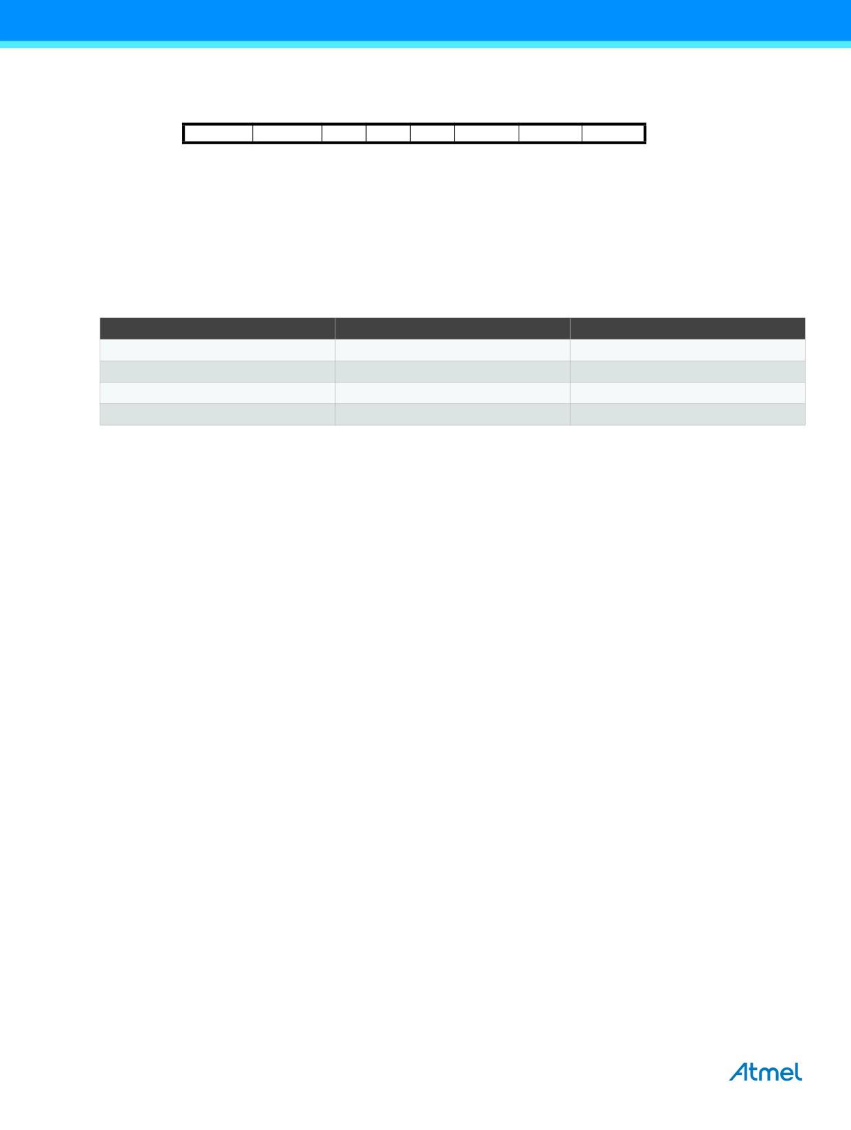
UCSRnC - USART MSPIM Control and Status Register n C
Bit
7
6
5
4
3
2
1
0
UMSELn1
UMSELn0
-
-
-
UDORDn
UCPHAn
UCPOLn
UCSRnC
Read/Write
R/W
R/W
R
R
R
R/W
R/W
R/W
Initial Value
0
0
0
0
0
1
1
0
• Bit 7:6 - UMSELn1:0: USART Mode Select
These bits select the mode of operation of the USART as shown in Table 20-4. See Section 19.10.4 “UCSRnC - USART
Control and Status Register n C” on page 161 for full description of the normal USART operation. The MSPIM is enabled
when both UMSELn bits are set to one. The UDORDn, UCPHAn, and UCPOLn can be set in the same write operation where
the MSPIM is enabled.
Table 20-4. UMSELn Bits Settings
UMSELn1
UMSELn0
Mode
0
0
Asynchronous USART
0
1
Synchronous USART
1
0
Reserved
1
1
Master SPI (MSPIM)
• Bit 5:3 - Reserved Bits in MSPI mode
When in MSPI mode, these bits are reserved for future use. For compatibility with future devices, these bits must be written
to zero when UCSRnC is written.
• Bit 2 - UDORDn: Data Order
When set to one the LSB of the data word is transmitted first. When set to zero the MSB of the data word is transmitted first.
Refer to the frame formats section page 4 for details.
• Bit 1 - UCPHAn: Clock Phase
The UCPHAn bit setting determine if data is sampled on the leasing edge (first) or tailing (last) edge of XCKn. Refer to the
SPI data modes and timing section page 4 for details.
• Bit 0 - UCPOLn: Clock Polarity
The UCPOLn bit sets the polarity of the XCKn clock. The combination of the UCPOLn and UCPHAn bit settings determine
the timing of the data transfer. Refer to the SPI data modes and timing section page 4 for details.
20.8.5
USART MSPIM Baud Rate Registers - UBRRnL and UBRRnH
The function and bit description of the baud rate registers in MSPI mode is identical to normal USART operation. See
Section 19.10.5 “UBRRnL and UBRRnH - USART Baud Rate Registers” on page 162.
172
ATmega328P [DATASHEET]
7810D-AVR-01/15
21.
2-wire Serial Interface
21.1
Features
● Simple yet powerful and flexible communication interface, only two bus lines needed
● Both master and slave operation supported
● Device can operate as transmitter or receiver
●
7-bit address space allows up to 128 different slave addresses
● Multi-master arbitration support
● Up to 400kHz data transfer speed
● Slew-rate limited output drivers
● Noise suppression circuitry rejects spikes on bus lines
● Fully programmable slave address with general call support
● Address recognition causes wake-up when AVR® is in sleep mode
● Compatible with Phillips’ I2C protocol
21.2
2-wire Serial Interface Bus Definition
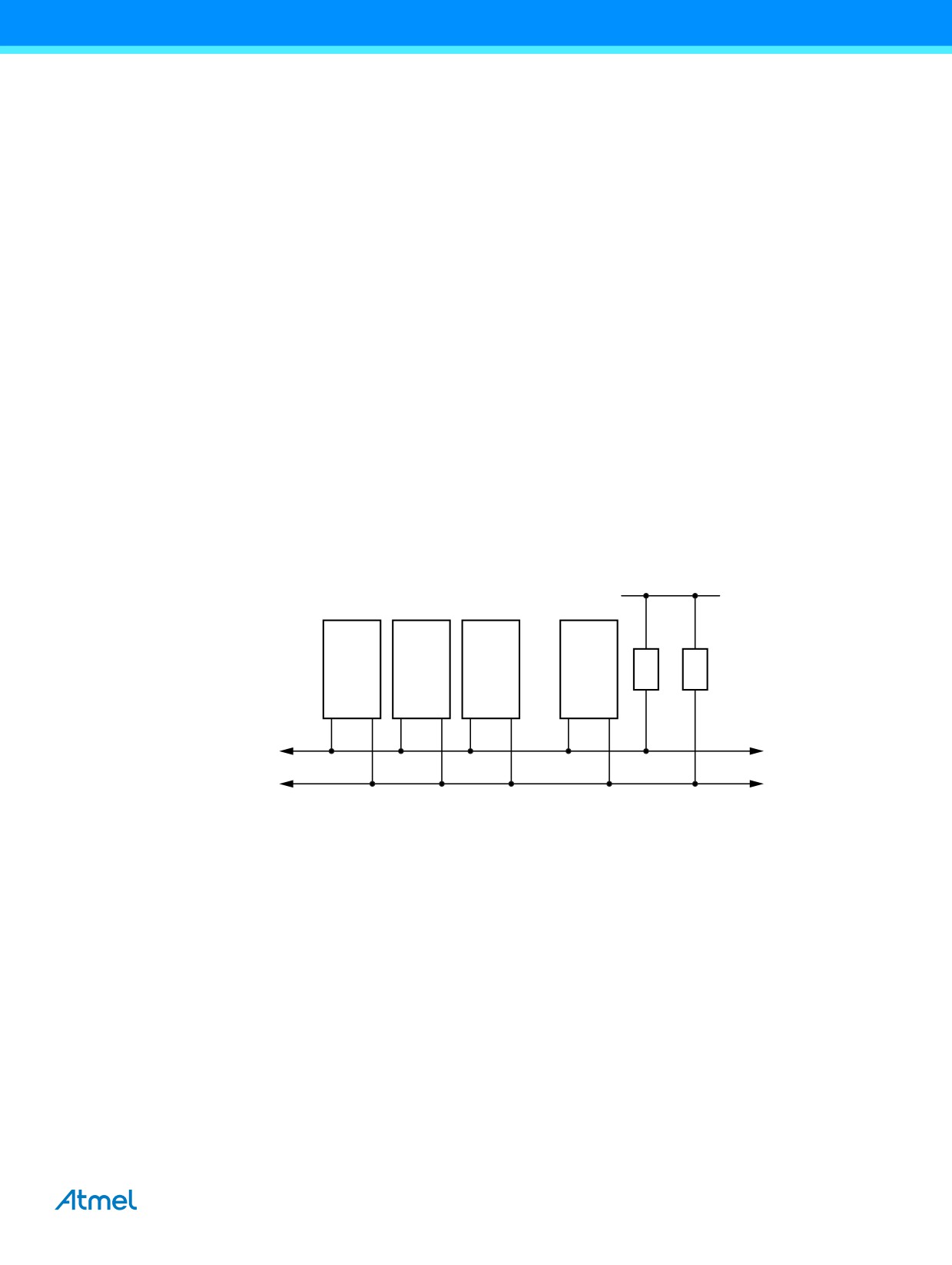
The 2-wire serial interface (TWI) is ideally suited for typical microcontroller applications. The TWI protocol allows the
systems designer to interconnect up to 128 different devices using only two bi-directional bus lines, one for clock (SCL) and
one for data (SDA). The only external hardware needed to implement the bus is a single pull-up resistor for each of the TWI
bus lines. All devices connected to the bus have individual addresses, and mechanisms for resolving bus contention are
inherent in the TWI protocol.
Figure 21-1. TWI Bus Interconnection
VCC
Device 1
Device 2
Device 3
Device n
R1
R2
SDA
SCL
ATmega328P [DATASHEET]
173
7810D-AVR-01/15
21.2.1
TWI Terminology
The following definitions are frequently encountered in this section.
Table 21-1. TWI Terminology
Term
Description
Master
The device that initiates and terminates a transmission. The master also generates the SCL clock.
Slave
The device addressed by a master.
Transmitter
The device placing data on the bus.
Receiver
The device reading data from the bus.
The PRTWI bit in Section 9.10 “Minimizing Power Consumption” on page 36 must be written to zero to enable the 2-wire
serial interface.
21.2.2
Electrical Interconnection
As depicted in Figure 21-1 on page 173, both bus lines are connected to the positive supply voltage through pull-up
resistors. The bus drivers of all TWI-compliant devices are open-drain or open-collector. This implements a wired-AND
function which is essential to the operation of the interface. A low level on a TWI bus line is generated when one or more TWI
devices output a zero. A high level is output when all TWI devices tri-state their outputs, allowing the pull-up resistors to pull
the line high. Note that all AVR® devices connected to the TWI bus must be powered in order to allow any bus operation.
The number of devices that can be connected to the bus is only limited by the bus capacitance limit of 400pF and the 7-bit
slave address space. A detailed specification of the electrical characteristics of the TWI is given in Section 28.8 “2-wire
Serial Interface Characteristics” on page 264. Two different sets of specifications are presented there, one relevant for bus
speeds below 100kHz, and one valid for bus speeds up to 400kHz.
21.3
Data Transfer and Frame Format
21.3.1
Transferring Bits
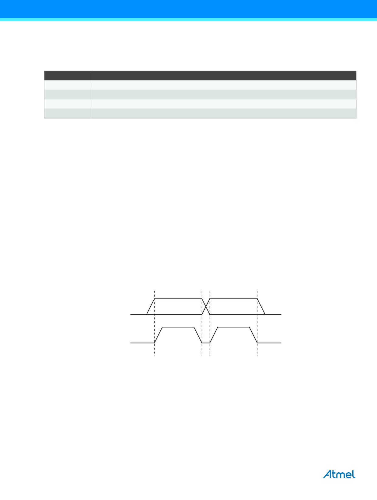
Each data bit transferred on the TWI bus is accompanied by a pulse on the clock line. The level of the data line must be
stable when the clock line is high. The only exception to this rule is for generating start and stop conditions.
Figure 21-2. Data Validity
SDA
SCL
Data Stable
Data Stable
Data Change
174
ATmega328P [DATASHEET]
7810D-AVR-01/15
21.3.2
START and STOP Conditions
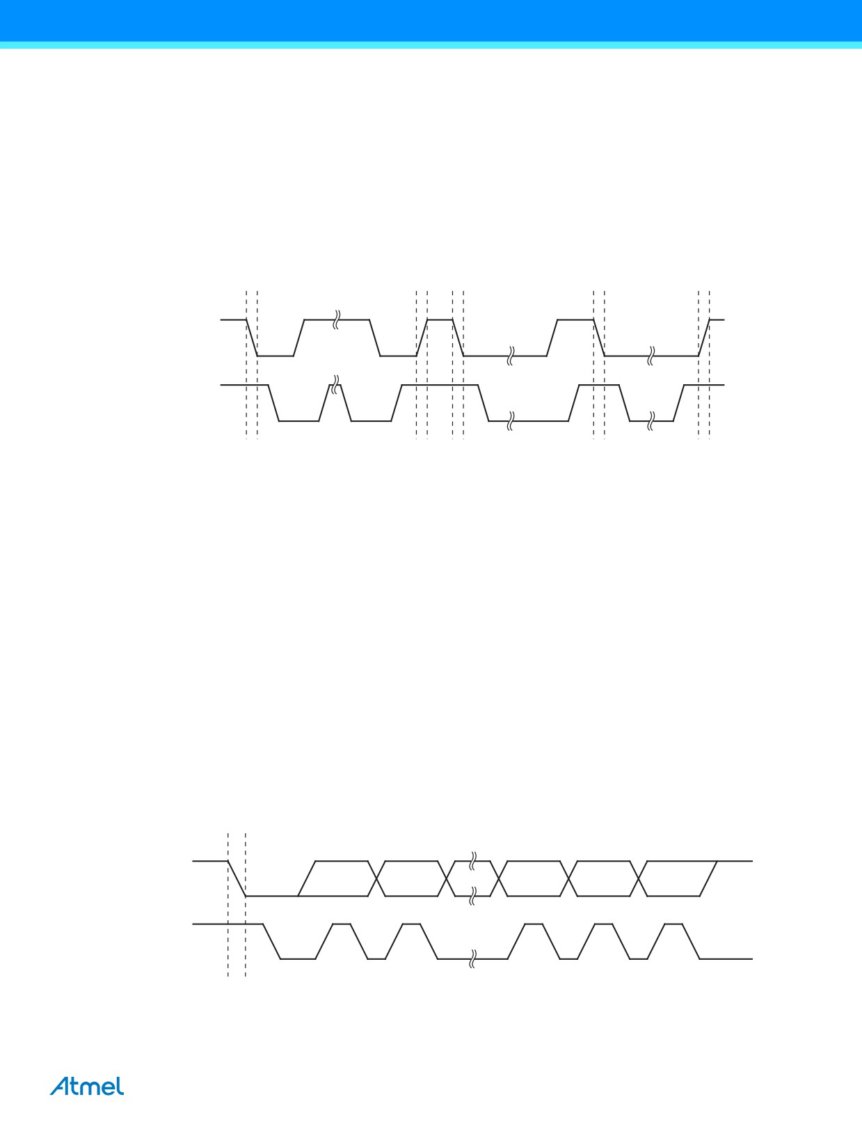
The master initiates and terminates a data transmission. The transmission is initiated when the master issues a START
condition on the bus, and it is terminated when the master issues a STOP condition. Between a START and a STOP
condition, the bus is considered busy, and no other master should try to seize control of the bus. A special case occurs when
a new START condition is issued between a START and STOP condition. This is referred to as a REPEATED START
condition, and is used when the master wishes to initiate a new transfer without relinquishing control of the bus. After a
REPEATED START, the bus is considered busy until the next STOP. This is identical to the START behavior, and therefore
START is used to describe both START and REPEATED START for the remainder of this datasheet, unless otherwise
noted. As depicted below, START and STOP conditions are signalled by changing the level of the SDA line when the SCL
line is high.
Figure 21-3. START, REPEATED START and STOP Conditions
SDA
SCL
START
STOP START
REPEATED START
STOP
21.3.3
Address Packet Format
All address packets transmitted on the TWI bus are 9 bits long, consisting of 7 address bits, one READ/WRITE control bit
and an acknowledge bit. If the READ/WRITE bit is set, a read operation is to be performed, otherwise a write operation
should be performed. When a slave recognizes that it is being addressed, it should acknowledge by pulling SDA low in the
ninth SCL (ACK) cycle. If the addressed Slave is busy, or for some other reason can not service the master’s request, the
SDA line should be left high in the ACK clock cycle. The master can then transmit a STOP condition, or a REPEATED
START condition to initiate a new transmission. An address packet consisting of a slave address and a READ or a WRITE
bit is called SLA+R or SLA+W, respectively.
The MSB of the address byte is transmitted first. Slave addresses can freely be allocated by the designer, but the address
0000 000 is reserved for a general call.
When a general call is issued, all slaves should respond by pulling the SDA line low in the ACK cycle. A general call is used
when a master wishes to transmit the same message to several slaves in the system. When the general call address
followed by a write bit is transmitted on the bus, all slaves set up to acknowledge the general call will pull the SDA line low in
the ack cycle. The following data packets will then be received by all the slaves that acknowledged the general call. Note that
transmitting the general call address followed by a read bit is meaningless, as this would cause contention if several slaves
started transmitting different data.
All addresses of the format 1111 xxx should be reserved for future purposes.
Figure 21-4. Address Packet Format
Addr MSB
Addr LSB
R/W
ACK
SDA
SCL
1
2
7
8
9
START
ATmega328P [DATASHEET]
175
7810D-AVR-01/15
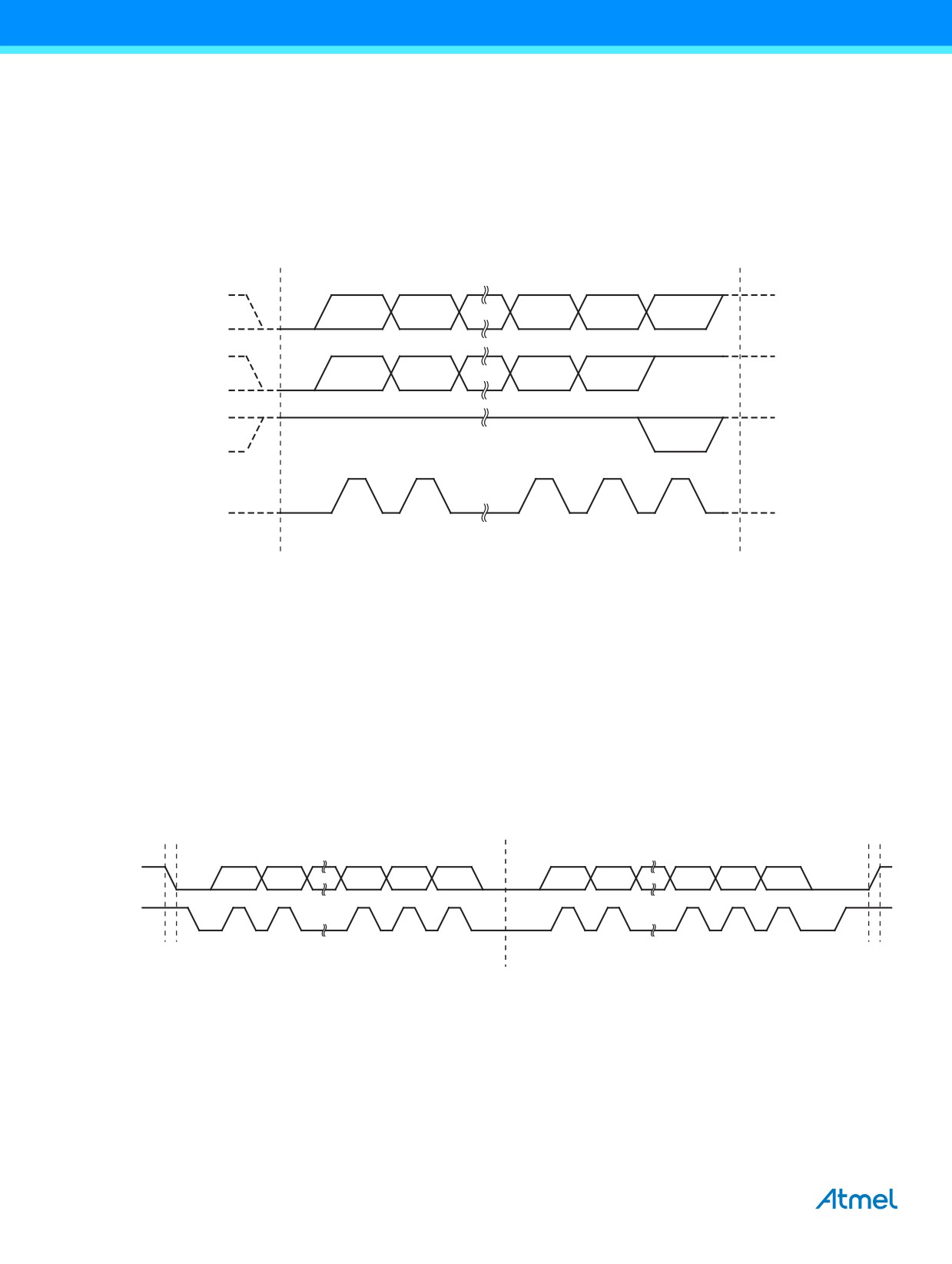
21.3.4
Data Packet Format
All data packets transmitted on the TWI bus are nine bits long, consisting of one data byte and an acknowledge bit. During a
data transfer, the master generates the clock and the START and STOP conditions, while the receiver is responsible for
acknowledging the reception. An acknowledge (ACK) is signalled by the receiver pulling the SDA line low during the ninth
SCL cycle. If the receiver leaves the SDA line high, a NACK is signalled. When the receiver has received the last byte, or for
some reason cannot receive any more bytes, it should inform the transmitter by sending a NACK after the final byte. The
MSB of the data byte is transmitted first.
Figure 21-5. Data Packet Format
Data MSB
Data LSB
ACK
Aggregate
SDA
SDA from
Transmitter
SDA from
Receiver
SCL from
Master
1
2
7
8
9
STOP, REPEATED
SLA + R/W
Data Byte
START or next
Data Byte
21.3.5
Combining Address and Data Packets into a Transmission
A transmission basically consists of a START condition, a SLA+R/W, one or more data packets and a STOP condition. An
empty message, consisting of a START followed by a STOP condition, is illegal. Note that the Wired-ANDing of the SCL line
can be used to implement handshaking between the master and the slave. The slave can extend the SCL low period by
pulling the SCL line low. This is useful if the clock speed set up by the master is too fast for the slave, or the slave needs
extra time for processing between the data transmissions. The slave extending the SCL low period will not affect the SCL
high period, which is determined by the master. As a consequence, the slave can reduce the TWI data transfer speed by
prolonging the SCL duty cycle.
Figure 21-6 shows a typical data transmission. Note that several data bytes can be transmitted between the SLA+R/W and
the STOP condition, depending on the software protocol implemented by the application software.
Figure 21-6. Typical Data Transmission
Addr MSB
Addr LSB R/W
ACK
Data MSB
Data LSB ACK
SDA
SCL
1
2
7
8
9
1
2
7
8
9
START
SLA + R/W
Data Byte
STOP
176
ATmega328P [DATASHEET]
7810D-AVR-01/15
21.4
Multi-master Bus Systems, Arbitration and Synchronization
The TWI protocol allows bus systems with several masters. Special concerns have been taken in order to ensure that
transmissions will proceed as normal, even if two or more masters initiate a transmission at the same time. Two problems
arise in multi-master systems:
● An algorithm must be implemented allowing only one of the masters to complete the transmission. All other masters
should cease transmission when they discover that they have lost the selection process. This selection process is
called arbitration. When a contending master discovers that it has lost the arbitration process, it should immediately
switch to slave mode to check whether it is being addressed by the winning master. The fact that multiple masters
have started transmission at the same time should not be detectable to the slaves, i.e. the data being transferred on
the bus must not be corrupted.
● Different masters may use different SCL frequencies. A scheme must be devised to synchronize the serial clocks
from all masters, in order to let the transmission proceed in a lockstep fashion. This will facilitate the arbitration
process.
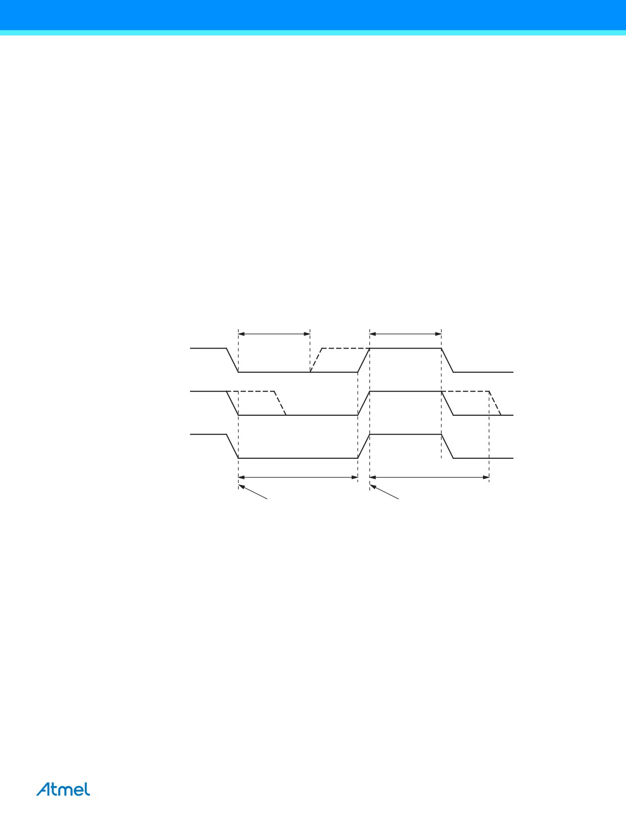
The wired-ANDing of the bus lines is used to solve both these problems. The serial clocks from all masters will be wired-
ANDed, yielding a combined clock with a high period equal to the one from the master with the shortest high period. The low
period of the combined clock is equal to the low period of the master with the longest low period. Note that all masters listen
to the SCL line, effectively starting to count their SCL high and low time-out periods when the combined SCL line goes high
or low, respectively.
Figure 21-7. SCL Synchronization Between Multiple Masters
TAlow
TAhigh
SCL from
Master A
SCL from
Master B
SCL Bus
Line
TBlow
TBhigh
Masters Start
Masters Start
Counting Low Period
Counting High Period
Arbitration is carried out by all masters continuously monitoring the SDA line after outputting data. If the value read from the
SDA line does not match the value the master had output, it has lost the arbitration. Note that a master can only lose
arbitration when it outputs a high SDA value while another master outputs a low value. The losing master should
immediately go to slave mode, checking if it is being addressed by the winning master. The SDA line should be left high, but
losing masters are allowed to generate a clock signal until the end of the current data or address packet.
Arbitration will continue until only one master remains, and this may take many bits. If several masters are trying to address
the same slave, arbitration will continue into the data packet.
ATmega328P [DATASHEET]
177
7810D-AVR-01/15
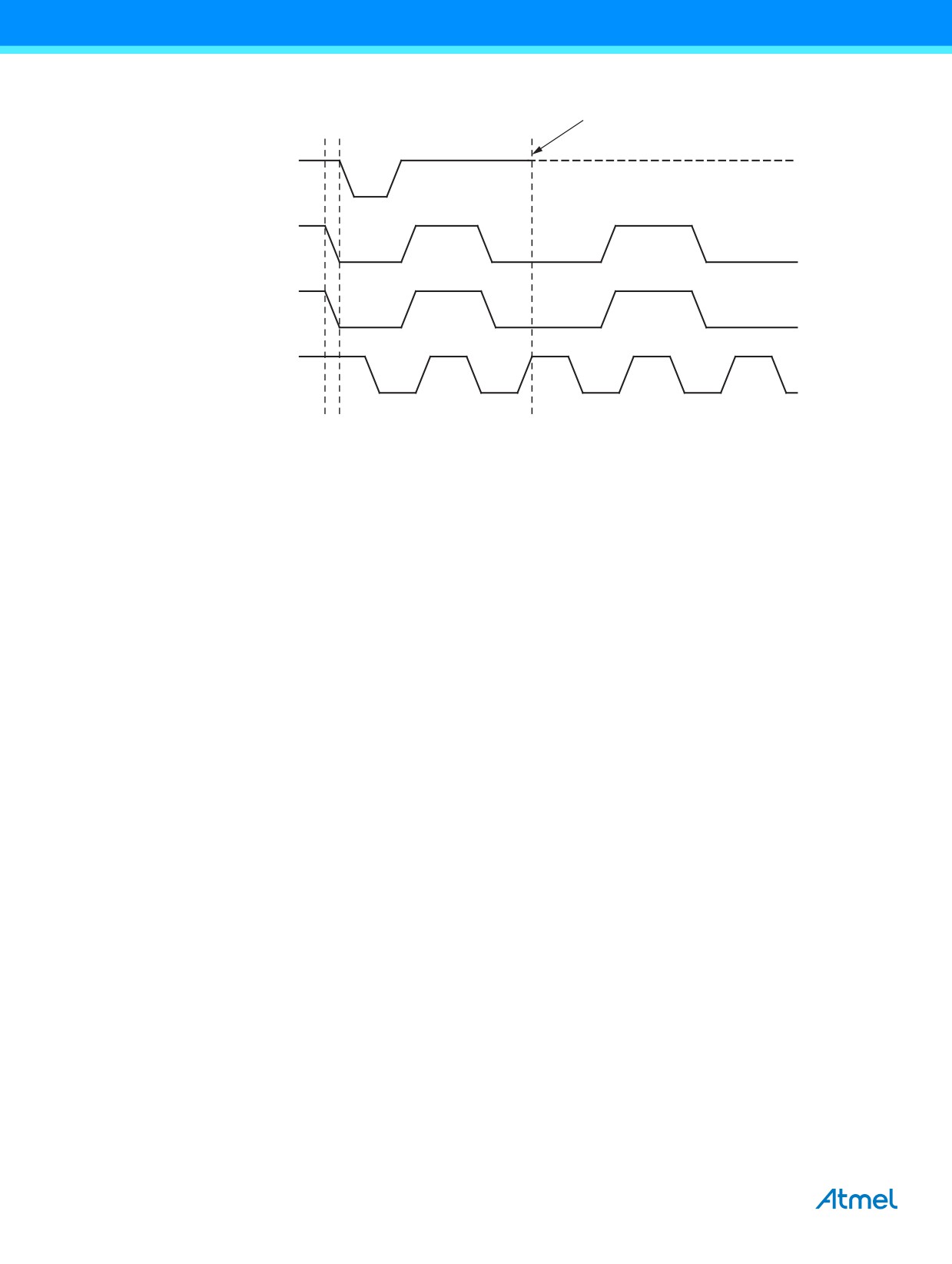
Figure 21-8. Arbitration Between Two Masters
Master A Loses
START
Arbitration, SDAA ≠ SDA
SDA from
Master A
SDA from
Master B
SDA Line
Synchronized
SCL Line
Note that arbitration is not allowed between:
● A REPEATED START condition and a data bit.
● A STOP condition and a data bit.
● A REPEATED START and a STOP condition.
It is the user software’s responsibility to ensure that these illegal arbitration conditions never occur. This implies that in
multi-master systems, all data transfers must use the same composition of SLA+R/W and data packets. In other words: All
transmissions must contain the same number of data packets, otherwise the result of the arbitration is undefined.
178
ATmega328P [DATASHEET]
7810D-AVR-01/15
21.5
Overview of the TWI Module
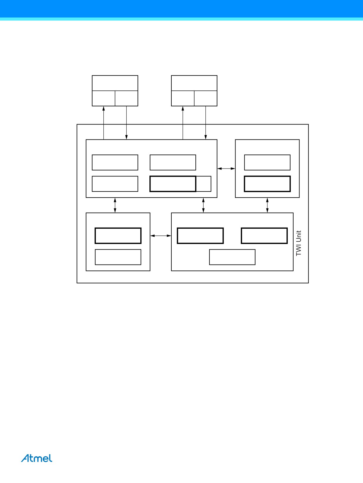
The TWI module is comprised of several sub modules, as shown in Figure 21-9. All registers drawn in a thick line are
accessible through the AVR® data bus.
Figure 21-9. Overview of the TWI Module
SCL
SDA
Slew-rate
Spike
Slew-rate
Spike
Control
Filter
Control
Filter
Bus Interface Unit
Bit Rate Generator
START/ STOP
Spike Suppression
Prescaler
Control
Address/ Data Shift
Bit Rate Register
Arbitration detection
Ack
Register (TWDR)
(TWBR)
Address Match Unit
Control Unit
Address Register
Status Register
Control Register
(TWAR)
(TWSR)
(TWCR)
State Machine and
Address Comparator
Status control
21.5.1
SCL and SDA Pins
These pins interface the AVR TWI with the rest of the MCU system. The output drivers contain a slew-rate limiter in order to
conform to the TWI specification. The input stages contain a spike suppression unit removing spikes shorter than 50ns. Note
that the internal pull-ups in the AVR pads can be enabled by setting the PORT bits corresponding to the SCL and SDA pins,
as explained in the I/O port section. The internal pull-ups can in some systems eliminate the need for external ones.
ATmega328P [DATASHEET]
179
7810D-AVR-01/15
21.5.2
Bit Rate Generator Unit
This unit controls the period of SCL when operating in a master mode. The SCL period is controlled by settings in the TWI bit
rate register (TWBR) and the prescaler bits in the TWI status register (TWSR). Slave operation does not depend on bit rate
or prescaler settings, but the CPU clock frequency in the slave must be at least 16 times higher than the SCL frequency.
Note that slaves may prolong the SCL low period, thereby reducing the average TWI bus clock period. The SCL frequency is
generated according to the following equation:
SCL frequency
= -------------------------------------------------------------------------------------
16 + 2TWBR PrescalerValue
● TWBR = Value of the TWI Bit rate register.
● PrescalerValue = Value of the prescaler, see Table 21-8 on page 200.
Note:
Pull-up resistor values should be selected according to the SCL frequency and the capacitive bus line load.
See Table 28-7 on page 264 for value of pull-up resistor.
21.5.3
Bus Interface Unit
This unit contains the data and address shift register (TWDR), a START/STOP controller and arbitration detection hardware.
The TWDR contains the address or data bytes to be transmitted, or the address or data bytes received. In addition to the
8-bit TWDR, the bus interface unit also contains a register containing the (N)ACK bit to be transmitted or received. This
(N)ACK register is not directly accessible by the application software. However, when receiving, it can be set or cleared by
manipulating the TWI control register (TWCR). When in transmitter mode, the value of the received (N)ACK bit can be
determined by the value in the TWSR.
The START/STOP controller is responsible for generation and detection of START, REPEATED START, and STOP
conditions. The START/STOP controller is able to detect START and STOP conditions even when the AVR MCU is in one of
the sleep modes, enabling the MCU to wake up if addressed by a master.
If the TWI has initiated a transmission as master, the arbitration detection hardware continuously monitors the transmission
trying to determine if arbitration is in process. If the TWI has lost an arbitration, the control unit is informed. Correct action
can then be taken and appropriate status codes generated.
21.5.4
Address Match Unit
The address match unit checks if received address bytes match the seven-bit address in the TWI address register (TWAR).
If the TWI general call recognition enable (TWGCE) bit in the TWAR is written to one, all incoming address bits will also be
compared against the general call address. Upon an address match, the control unit is informed, allowing correct action to
be taken. The TWI may or may not acknowledge its address, depending on settings in the TWCR. The address match unit is
able to compare addresses even when the AVR® MCU is in sleep mode, enabling the MCU to wake up if addressed by a
master.
If another interrupt (e.g., INT0) occurs during TWI power-down address match and wakes up the CPU, the TWI aborts
operation and return to it’s idle state. If this cause any problems, ensure that TWI Address Match is the only enabled
interrupt when entering power-down.
180
ATmega328P [DATASHEET]
7810D-AVR-01/15
21.5.5
Control Unit
The control unit monitors the TWI bus and generates responses corresponding to settings in the TWI control register
(TWCR). When an event requiring the attention of the application occurs on the TWI bus, the TWI interrupt flag (TWINT) is
asserted. In the next clock cycle, the TWI status register (TWSR) is updated with a status code identifying the event. The
TWSR only contains relevant status information when the TWI interrupt flag is asserted. At all other times, the TWSR
contains a special status code indicating that no relevant status information is available. As long as the TWINT flag is set, the
SCL line is held low. This allows the application software to complete its tasks before allowing the TWI transmission to
continue.
The TWINT flag is set in the following situations:
● After the TWI has transmitted a START/REPEATED START condition.
● After the TWI has transmitted SLA+R/W.
● After the TWI has transmitted an address byte.
● After the TWI has lost arbitration.
● After the TWI has been addressed by own slave address or general call.
● After the TWI has received a data byte.
● After a STOP or REPEATED START has been received while still addressed as a slave.
● When a bus error has occurred due to an illegal START or STOP condition.
21.6
Using the TWI
The AVR® TWI is byte-oriented and interrupt based. Interrupts are issued after all bus events, like reception of a byte or
transmission of a START condition. Because the TWI is interrupt-based, the application software is free to carry on other
operations during a TWI byte transfer. Note that the TWI interrupt enable (TWIE) bit in TWCR together with the global
interrupt enable bit in SREG allow the application to decide whether or not assertion of the TWINT flag should generate an
interrupt request. If the TWIE bit is cleared, the application must poll the TWINT flag in order to detect actions on the TWI
bus.
When the TWINT flag is asserted, the TWI has finished an operation and awaits application response. In this case, the TWI
status register (TWSR) contains a value indicating the current state of the TWI bus. The application software can then
decide how the TWI should behave in the next TWI bus cycle by manipulating the TWCR and TWDR registers.
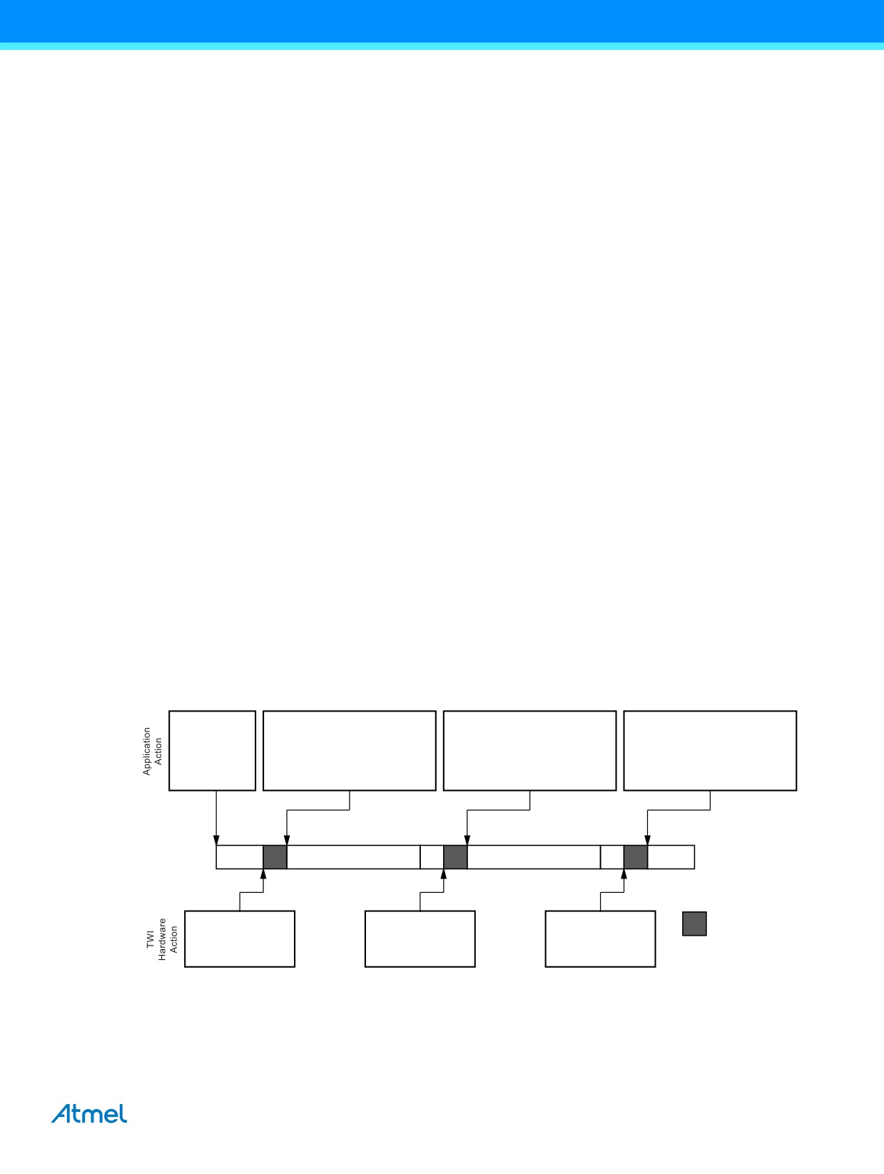
Figure 21-10 is a simple example of how the application can interface to the TWI hardware. In this example, a master wishes
to transmit a single data byte to a slave. This description is quite abstract, a more detailed explanation follows later in this
section. A simple code example implementing the desired behavior is also presented.
Figure 21-10. Interfacing the Application to the TWI in a Typical Transmission
3. Check TWSR to see if START was
5. Check TWSR to see if SLA + W was
7. Check TWSR to see if data was sent
1. Application
sent. Application loads SLA + W into
sent and ACK received.
and ACK received.
writes to TWCR to
TWDR, and loads appropriate control
Application loads data intoTWDR, and
Application loads appropriate control
initiate
signals into TWCR, making sure that
loads appropriate control signals into
signals to send STOP into TWCR,
transmission of
TWINT is written to one,
TWCR, making sure that TWINT is
makin sure that TWINT is
START
and TWSTA is written to zero.
written to one
written to one
TWI bus
START
SLA + W
A
Data
A
STOP
Indicates
4. TWINT set.
2. TWINT set.
6. TWINT set.
TWINT set
Status code indicates
Status code indicates
Status code indicates
SLA + W sent,
START condition sent
data sent, ACK received
ACK received
ATmega328P [DATASHEET]
181
7810D-AVR-01/15
1.
The first step in a TWI transmission is to transmit a START condition. This is done by writing a specific value into
TWCR, instructing the TWI hardware to transmit a START condition. Which value to write is described later on.
However, it is important that the TWINT bit is set in the value written. Writing a one to TWINT clears the flag. The
TWI will not start any operation as long as the TWINT bit in TWCR is set. Immediately after the application has
cleared TWINT, the TWI will initiate transmission of the START condition.
2.
When the START condition has been transmitted, the TWINT flag in TWCR is set, and TWSR is updated with a
status code indicating that the START condition has successfully been sent.
3.
The application software should now examine the value of TWSR, to make sure that the START condition was
successfully transmitted. If TWSR indicates otherwise, the application software might take some special action,
like calling an error routine. Assuming that the status code is as expected, the application must load SLA+W into
TWDR. Remember that TWDR is used both for address and data. After TWDR has been loaded with the desired
SLA+W, a specific value must be written to TWCR, instructing the TWI hardware to transmit the SLA+W present in
TWDR. Which value to write is described later on. However, it is important that the TWINT bit is set in the value
written. Writing a one to TWINT clears the flag. The TWI will not start any operation as long as the TWINT bit in
TWCR is set. Immediately after the application has cleared TWINT, the TWI will initiate transmission of the
address packet.
4.
When the address packet has been transmitted, the TWINT flag in TWCR is set, and TWSR is updated with a
status code indicating that the address packet has successfully been sent. The status code will also reflect
whether a slave acknowledged the packet or not.
5.
The application software should now examine the value of TWSR, to make sure that the address packet was
successfully transmitted, and that the value of the ACK bit was as expected. If TWSR indicates otherwise, the
application software might take some special action, like calling an error routine. Assuming that the status code is
as expected, the application must load a data packet into TWDR. Subsequently, a specific value must be written to
TWCR, instructing the TWI hardware to transmit the data packet present in TWDR. Which value to write is
described later on.
However, it is important that the TWINT bit is set in the value written. Writing a one to TWINT clears the flag. The
TWI will not start any operation as long as the TWINT bit in TWCR is set. Immediately after the application has
cleared TWINT, the TWI will initiate transmission of the data packet.
6.
When the data packet has been transmitted, the TWINT flag in TWCR is set, and TWSR is updated with a status
code indicating that the data packet has successfully been sent. The status code will also reflect whether a slave
acknowledged the packet or not.
7.
The application software should now examine the value of TWSR, to make sure that the data packet was
successfully transmitted, and that the value of the ACK bit was as expected. If TWSR indicates otherwise, the
application software might take some special action, like calling an error routine. Assuming that the status code is
as expected, the application must write a specific value to TWCR, instructing the TWI hardware to transmit a
STOP condition. Which value to write is described later on. However, it is important that the TWINT bit is set in the
value written. Writing a one to TWINT clears the flag. The TWI will not start any operation as long as the TWINT bit
in TWCR is set. Immediately after the application has cleared TWINT, the TWI will initiate transmission of the
STOP condition. Note that TWINT is NOT set after a STOP condition has been sent.
Even though this example is simple, it shows the principles involved in all TWI transmissions. These can be summarized as
follows:
● When the TWI has finished an operation and expects application response, the TWINT flag is set. The SCL line is
pulled low until TWINT is cleared.
● When the TWINT flag is set, the user must update all TWI registers with the value relevant for the next TWI bus cycle.
As an example, TWDR must be loaded with the value to be transmitted in the next bus cycle.
● After all TWI register updates and other pending application software tasks have been completed, TWCR is written.
When writing TWCR, the TWINT bit should be set. Writing a one to TWINT clears the flag. The TWI will then
commence executing whatever operation was specified by the TWCR setting.
182
ATmega328P [DATASHEET]
7810D-AVR-01/15

In the following an assembly and C implementation of the example is given. Note that the code below assumes that several
definitions have been made, for example by using include-files.
Table 21-2. Assembly code Example
Assembly Code Example
C Example
Comments
ldi
r16, (1<<TWINT)|(1<<TWSTA)|
TWCR = (1<<TWINT)|(1<<TWSTA)|
1
(1<<TWEN)
(1<<TWEN)
Send START condition
out
TWCR, r16
wait1:
while (!(TWCR & (1<<TWINT)))
Wait for TWINT flag set. This
in
r16,TWCR
;
2
indicates that the START
sbrs
r16,TWINT
condition has been transmitted
rjmp
wait1
in
r16,TWSR
if ((TWSR & 0xF8) != START)
Check value of TWI status
andi
r16, 0xF8
ERROR();
register. Mask prescaler bits. If
cpi
r16, START
status different from START go
brne
ERROR
to ERROR
3
ldi
r16, SLA_W
TWDR = SLA_W;
Load SLA_W into TWDR
out
TWDR, r16
TWCR = (1<<TWINT) |
register. Clear TWINT bit in
ldi
r16, (1<<TWINT) |
(1<<TWEN);
TWCR to start transmission of
(1<<TWEN)
address
out
TWCR, r16
wait2:
while (!(TWCR & (1<<TWINT)))
Wait for TWINT flag set. This
in
r16,TWCR
;
indicates that the SLA+W has
4
sbrs
r16,TWINT
been transmitted, and
rjmp
wait2
ACK/NACK has been received.
in
r16,TWSR
if ((TWSR & 0xF8) != MT_SLA_ACK)
Check value of TWI status
andi
r16, 0xF8
ERROR();
register. Mask prescaler bits. If
cpi
r16, MT_SLA_ACK
status different from
brne
ERROR
MT_SLA_ACK go to ERROR
5
ldi
r16, DATA
TWDR = DATA;
out
TWDR, r16
TWCR = (1<<TWINT) | (1<<TWEN);
Load DATA into TWDR register.
ldi
r16, (1<<TWINT) |
clear TWINT bit in TWCR to
(1<<TWEN)
start transmission of data
out
TWCR, r16
wait3:
while (!(TWCR & (1<<TWINT)))
Wait for TWINT flag set. This
in
r16,TWCR
;
indicates that the DATA has
6
sbrs
r16,TWINT
been transmitted, and
rjmp
wait3
ACK/NACK has been received.
in
r16,TWSR
if ((TWSR & 0xF8)!= MT_DATA_ACK)
Check value of TWI status
andi
r16, 0xF8
ERROR();
register. Mask prescaler bits. If
cpi
r16, MT_DATA_ACK
status different from
7
brne
ERROR
MT_DATA_ACK go to ERROR
ldi
r16, (1<<TWINT)|(1<<TWEN)|
TWCR = (1<<TWINT)|(1<<TWEN)|
(1<<TWSTO)
(1<<TWSTO);
Transmit STOP condition
out
TWCR, r16
ATmega328P [DATASHEET]
183
7810D-AVR-01/15
21.7
Transmission Modes
The TWI can operate in one of four major modes. These are named master transmitter (MT), master receiver (MR), slave
transmitter (ST) and slave receiver (SR). Several of these modes can be used in the same application. As an example, the
TWI can use MT mode to write data into a TWI EEPROM, MR mode to read the data back from the EEPROM. If other
masters are present in the system, some of these might transmit data to the TWI, and then SR mode would be used. It is the
application software that decides which modes are legal.
The following sections describe each of these modes. Possible status codes are described along with figures detailing data
transmission in each of the modes. These figures contain the following abbreviations:
S:
START condition
Rs:
REPEATED START condition
R:
Read bit (high level at SDA)
W:
Write bit (low level at SDA)
A:
Acknowledge bit (low level at SDA)
A:
Not acknowledge bit (high level at SDA)
Data:
8-bit data byte
P:
STOP condition
SLA: Slave address
In Figure 21-12 on page 187 to Figure 21-18 on page 196, circles are used to indicate that the TWINT flag is set. The
numbers in the circles show the status code held in TWSR, with the prescaler bits masked to zero. At these points, actions
must be taken by the application to continue or complete the TWI transfer. The TWI transfer is suspended until the TWINT
flag is cleared by software.
When the TWINT flag is set, the status code in TWSR is used to determine the appropriate software action. For each status
code, the required software action and details of the following serial transfer are given in Table 21-3 on page 186 to
Table 21-6 on page 195. Note that the prescaler bits are masked to zero in these tables.
21.7.1
Master Transmitter Mode
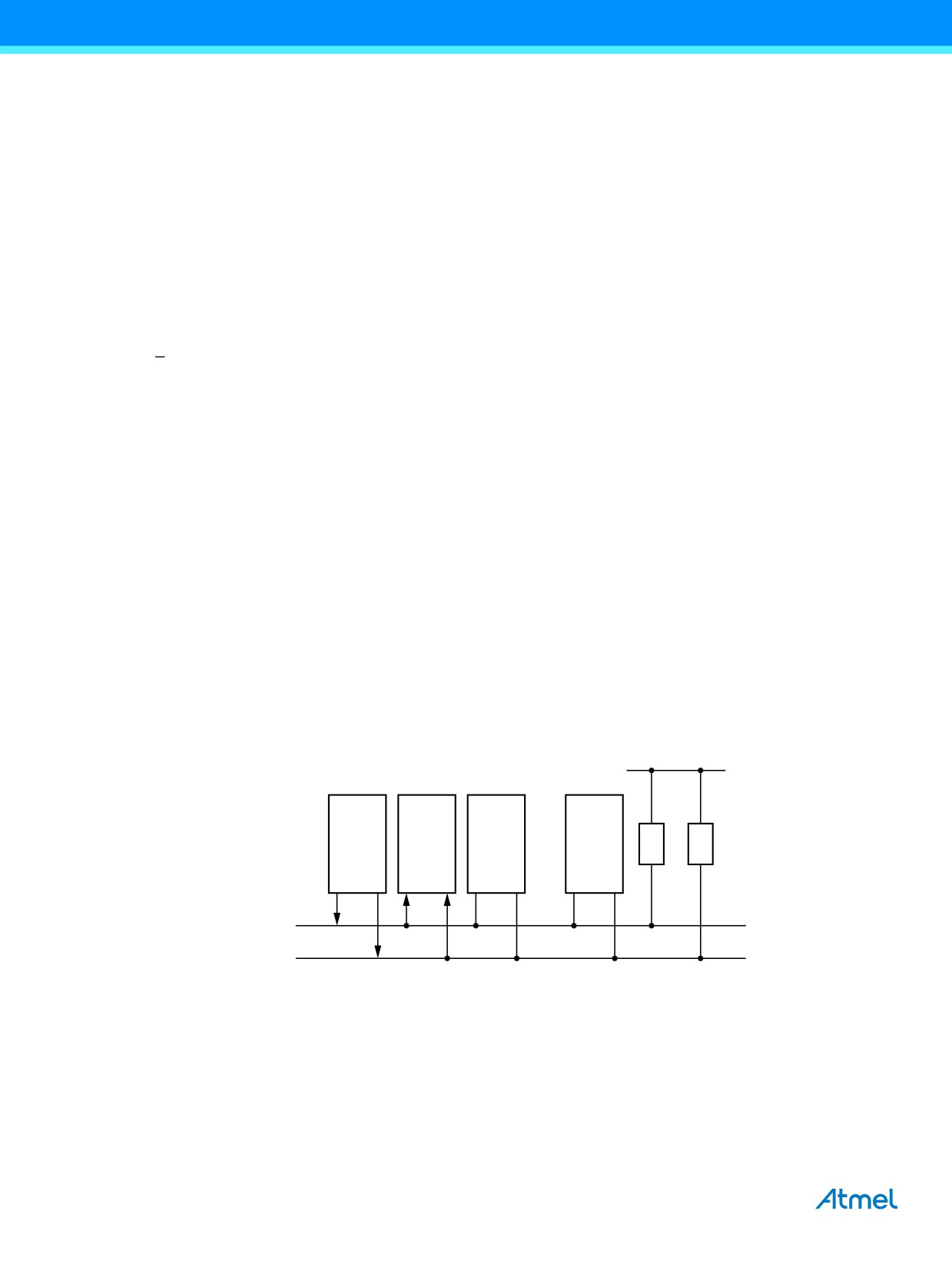
In the master transmitter mode, a number of data bytes are transmitted to a slave receiver (see Figure 21-11). In order to
enter a master mode, a START condition must be transmitted. The format of the following address packet determines
whether master transmitter or master receiver mode is to be entered. If SLA+W is transmitted, MT mode is entered, if SLA+R
is transmitted, MR mode is entered. All the status codes mentioned in this section assume that the prescaler bits are zero or
are masked to zero.
Figure 21-11. Data Transfer in Master Transmitter Mode
VCC
Device 1
Device 2
Master
Slave
Device 3
Device n
R1
R2
Transmitter
Receiver
SDA
SCL
184
ATmega328P [DATASHEET]
7810D-AVR-01/15
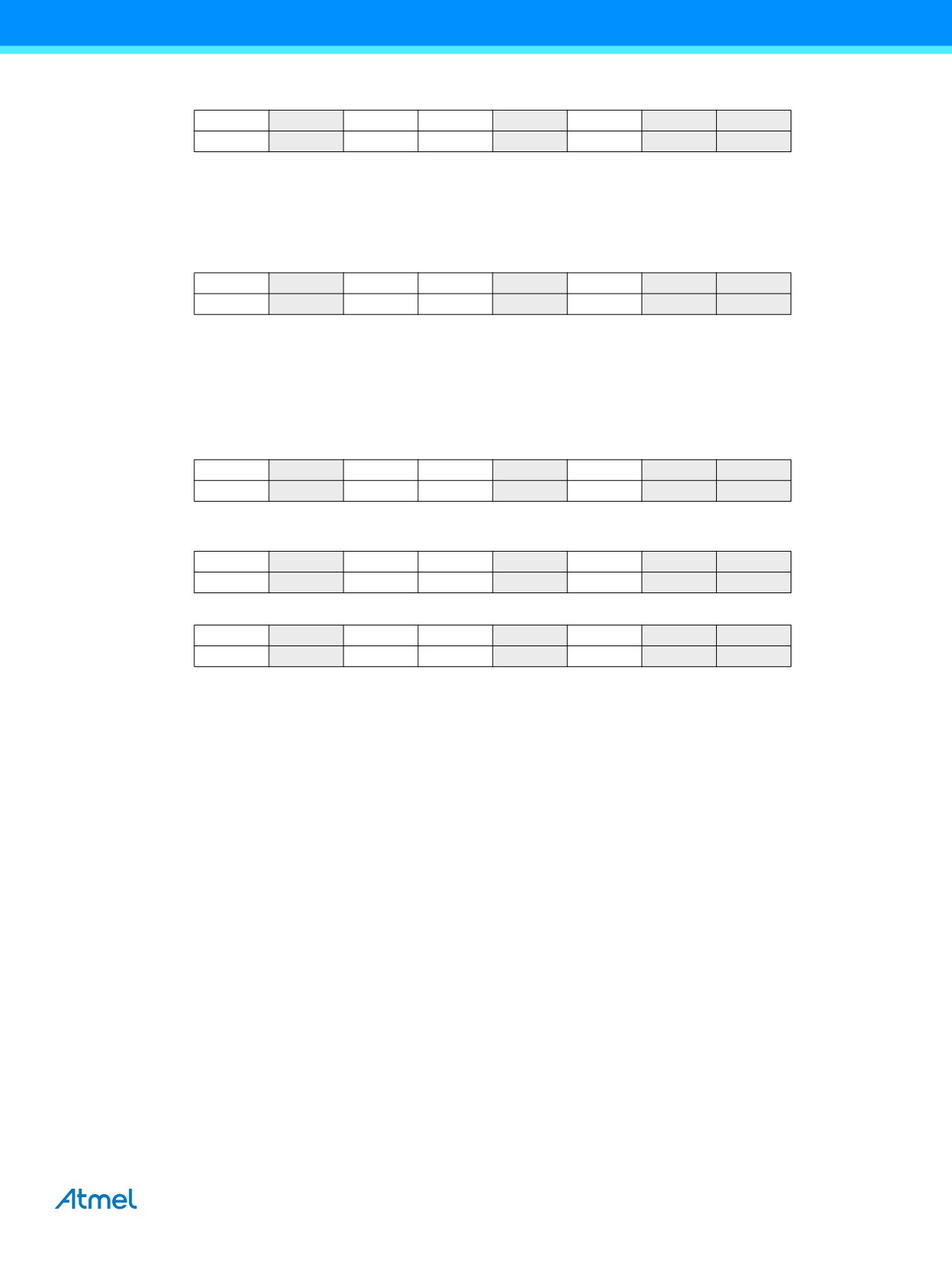
A START condition is sent by writing the following value to TWCR:
TWCR
TWINT
TWEA
TWSTA
TWSTO
TWWC
TWEN
-
TWIE
value
1
X
1
0
X
1
0
X
TWEN must be set to enable the 2-wire serial interface, TWSTA must be written to one to transmit a START condition and
TWINT must be written to one to clear the TWINT flag. The TWI will then test the 2-wire serial bus and generate a START
condition as soon as the bus becomes free. After a START condition has been transmitted, the TWINT flag is set by
hardware, and the status code in TWSR will be 0x08 (see Table 21-3). In order to enter MT mode, SLA+W must be
transmitted. This is done by writing SLA+W to TWDR. Thereafter the TWINT bit should be cleared (by writing it to one) to
continue the transfer. This is accomplished by writing the following value to TWCR:
TWCR
TWINT
TWEA
TWSTA
TWSTO
TWWC
TWEN
-
TWIE
value
1
X
0
0
X
1
0
X
When SLA+W have been transmitted and an acknowledgement bit has been received, TWINT is set again and a number of
status codes in TWSR are possible. Possible status codes in master mode are 0x18, 0x20, or 0x38. The appropriate action
to be taken for each of these status codes is detailed in Table 21-3.
When SLA+W has been successfully transmitted, a data packet should be transmitted. This is done by writing the data byte
to TWDR. TWDR must only be written when TWINT is high. If not, the access will be discarded, and the write collision bit
(TWWC) will be set in the TWCR register. After updating TWDR, the TWINT bit should be cleared (by writing it to one) to
continue the transfer. This is accomplished by writing the following value to TWCR:
TWCR
TWINT
TWEA
TWSTA
TWSTO
TWWC
TWEN
-
TWIE
value
1
X
0
0
X
1
0
X
This scheme is repeated until the last byte has been sent and the transfer is ended by generating a STOP condition or a
repeated START condition. A STOP condition is generated by writing the following value to TWCR:
TWCR
TWINT
TWEA
TWSTA
TWSTO
TWWC
TWEN
-
TWIE
value
1
X
0
1
X
1
0
X
A REPEATED START condition is generated by writing the following value to TWCR:
TWCR
TWINT
TWEA
TWSTA
TWSTO
TWWC
TWEN
-
TWIE
value
1
X
1
0
X
1
0
X
After a repeated START condition (state 0x10) the 2-wire serial interface can access the same slave again, or a new slave
without transmitting a STOP condition. Repeated START enables the master to switch between slaves, master transmitter
mode and master receiver mode without losing control of the bus.
ATmega328P [DATASHEET]
185
7810D-AVR-01/15
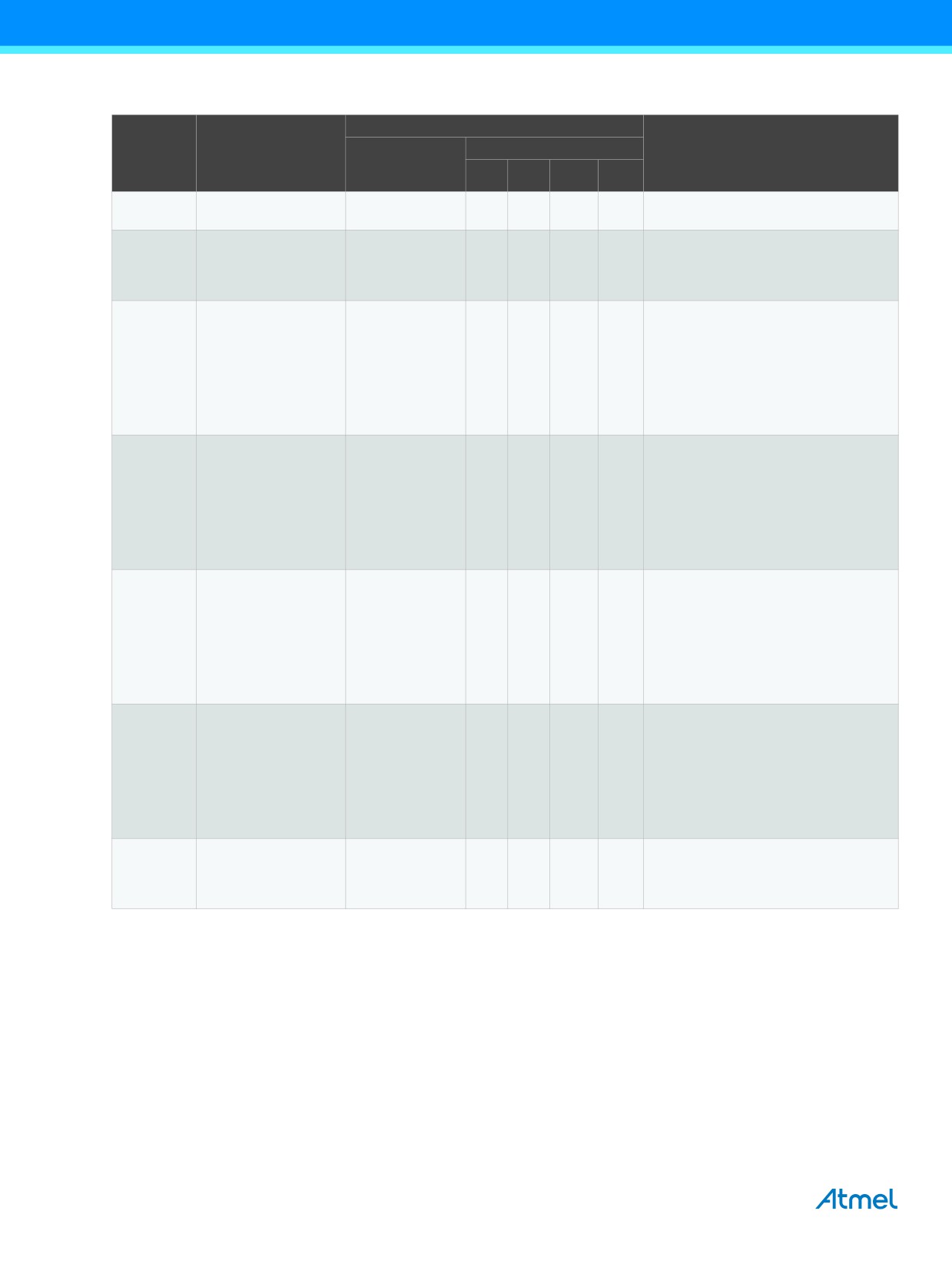
Table 21-3.
Status Codes for Master Transmitter Mode
Application Software Response
Status Code
Status of the 2-wire
(TWSR)
Serial Bus and 2-wire
To/from TWDR
To TWCR
Prescaler
Serial Interface
Bits are 0
Hardware
STA
STO
TWINT
TWEA
Next Action Taken by TWI Hardware
0x08
A START condition has
Load SLA+W
0
0
1
X
SLA+W will be transmitted;
been transmitted
ACK or NOT ACK will be received
0x10
A repeated START
Load SLA+W or
0
0
1
X
SLA+W will be transmitted;
condition has been
ACK or NOT ACK will be received
transmitted
Load SLA+R
0
0
1
X
SLA+R will be transmitted;
Logic will switch to master receiver mode
0x18
SLA+W has been
Load data byte or
0
0
1
X
Data byte will be transmitted and ACK or
transmitted; ACK has
NOT ACK will be received
been received
No TWDR action or
1
0
1
X
Repeated START will be transmitted
No TWDR action or
0
1
1
X
STOP condition will be transmitted and
TWSTO Flag will be reset
No TWDR action
1
1
1
X
STOP condition followed by a START
condition will be transmitted and TWSTO
flag will be reset
0x20
SLA+W has been
Load data byte or
0
0
1
X
Data byte will be transmitted and ACK or
transmitted; NOT ACK
NOT ACK will be received
has been received
No TWDR action or
1
0
1
X
Repeated START will be transmitted
No TWDR action or
0
1
1
X
STOP condition will be transmitted and
TWSTO flag will be reset
No TWDR action
1
1
1
X
STOP condition followed by a START
condition will be transmitted and TWSTO
flag will be reset
0x28
Data byte has been
Load data byte or
0
0
1
X
Data byte will be transmitted and ACK or
transmitted; ACK has
NOT ACK will be received
been received
No TWDR action or
1
0
1
X
Repeated START will be transmitted
No TWDR action or
0
1
1
X
STOP condition will be transmitted and
TWSTO flag will be reset
No TWDR action
1
1
1
X
STOP condition followed by a START
condition will be transmitted and TWSTO
flag will be reset
0x30
Data byte has been
Load data byte or
0
0
1
X
Data byte will be transmitted and ACK or
transmitted; NOT ACK
NOT ACK will be received
has been received
No TWDR action or
1
0
1
X
Repeated START will be transmitted
No TWDR action or
0
1
1
X
STOP condition will be transmitted and
TWSTO flag will be reset
No TWDR action
1
1
1
X
STOP condition followed by a START
condition will be transmitted and TWSTO
flag will be reset
0x38
Arbitration lost in SLA+W
No TWDR action or
0
0
1
X
2-wire Serial Bus will be released and not
or data bytes
addressed Slave mode entered
No TWDR action
1
0
1
X
A START condition will be transmitted when
the bus becomes free
186
ATmega328P [DATASHEET]
7810D-AVR-01/15
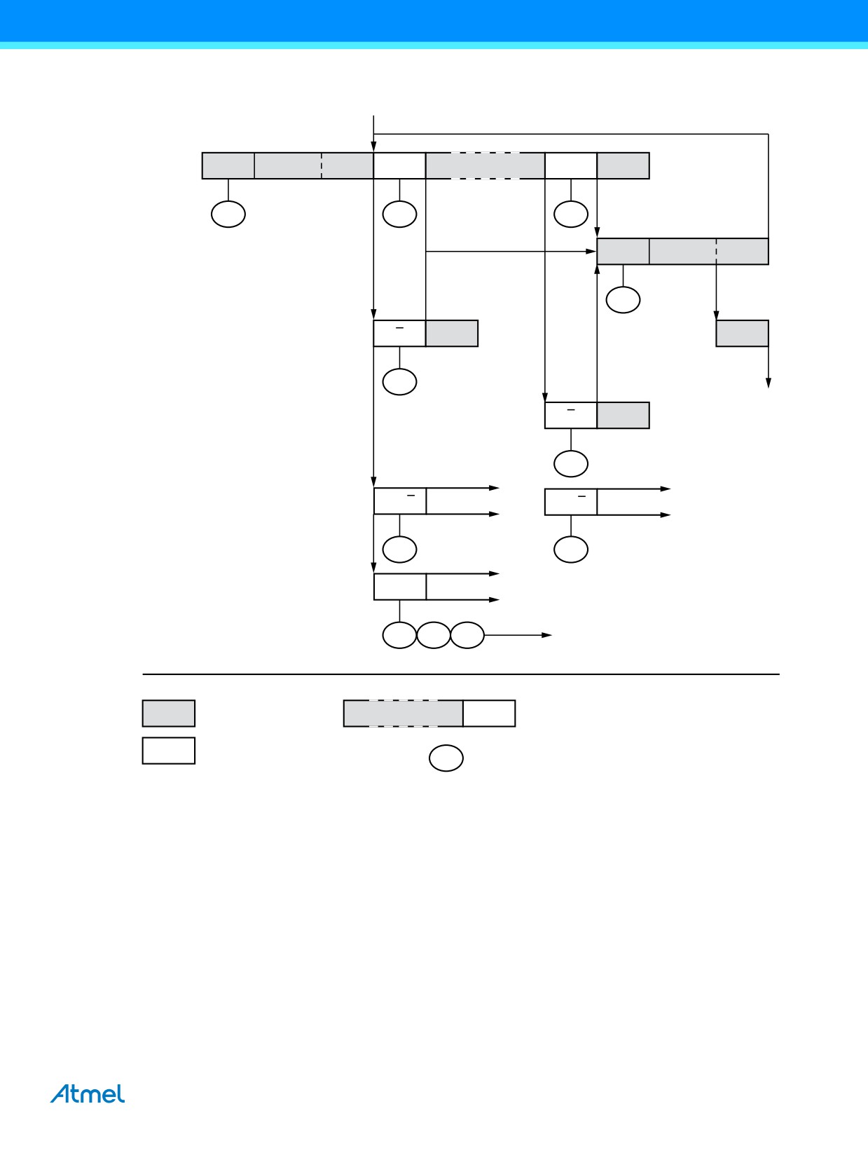
Figure 21-12. Formats and States in the Master Transmitter Mode
MT
Successfull
transmission
S
SLA
W
A
DATA
A
P
to a slave
receiver
$08
$18
$28
Next transfer
started with a
RS
SLA
W
repeated start
condition
$10
Not acknowledge
received after the
A
P
R
slave address
$20
MR
Not acknowledge
A
P
received after a
data byte
$30
Arbitration lost in slave
Other master
Other master
A or A
A or A
address or data byte
continues
continues
$38
$38
Arbitration lost and
Other master
A
addressed as slave
continues
To corresponding
$68
$78
$B0
states in slave mode
From master to slave
DATA
A
Any number of data bytes
and their associated acknowledge bits
From slave to master
This number (contained in TWSR) corresponds
n
to a defined state of the 2-Wire Serial Bus.
The prescaler bits are zero or masked to zero
ATmega328P [DATASHEET]
187
7810D-AVR-01/15
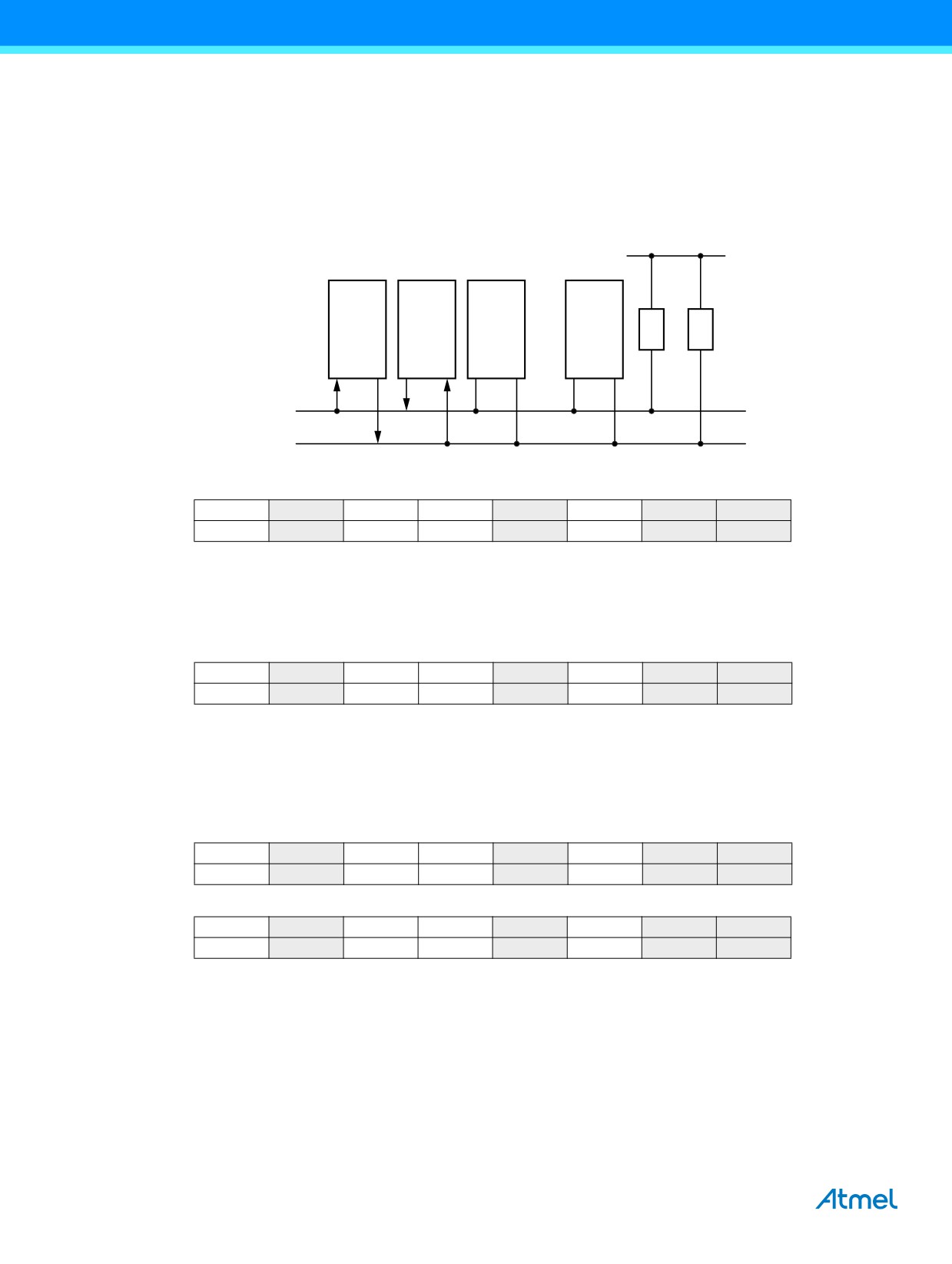
21.7.2
Master Receiver Mode
In the master receiver mode, a number of data bytes are received from a slave transmitter (slave see Figure 21-13). In order
to enter a master mode, a START condition must be transmitted. The format of the following address packet determines
whether master transmitter or master receiver mode is to be entered. If SLA+W is transmitted, MT mode is entered, if SLA+R
is transmitted, MR mode is entered. All the status codes mentioned in this section assume that the prescaler bits are zero or
are masked to zero.
Figure 21-13. Data Transfer in Master Receiver Mode
VCC
Device 1
Device 2
Master
Slave
Device 3
Device n
R1
R2
Receiver
Transmitter
SDA
SCL
A START condition is sent by writing the following value to TWCR:
TWCR
TWINT
TWEA
TWSTA
TWSTO
TWWC
TWEN
-
TWIE
value
1
X
1
0
X
1
0
X
TWEN must be written to one to enable the 2-wire serial interface, TWSTA must be written to one to transmit a START
condition and TWINT must be set to clear the TWINT flag. The TWI will then test the 2-wire serial bus and generate a
START condition as soon as the bus becomes free. After a START condition has been transmitted, the TWINT flag is set by
hardware, and the status code in TWSR will be 0x08 (See Table 21-3 on page 186). In order to enter MR mode, SLA+R must
be transmitted. This is done by writing SLA+R to TWDR. Thereafter the TWINT bit should be cleared (by writing it to one) to
continue the transfer. This is accomplished by writing the following value to TWCR:
TWCR
TWINT
TWEA
TWSTA
TWSTO
TWWC
TWEN
-
TWIE
value
1
X
0
0
X
1
0
X
When SLA+R have been transmitted and an acknowledgement bit has been received, TWINT is set again and a number of
status codes in TWSR are possible. Possible status codes in master mode are 0x38, 0x40, or 0x48. The appropriate action
to be taken for each of these status codes is detailed in Table 21-4 on page 189. Received data can be read from the TWDR
register when the TWINT flag is set high by hardware. This scheme is repeated until the last byte has been received. After
the last byte has been received, the MR should inform the ST by sending a NACK after the last received data byte. The
transfer is ended by generating a STOP condition or a repeated START condition. A STOP condition is generated by writing
the following value to TWCR:
TWCR
TWINT
TWEA
TWSTA
TWSTO
TWWC
TWEN
-
TWIE
value
1
X
0
1
X
1
0
X
A REPEATED START condition is generated by writing the following value to TWCR:
TWCR
TWINT
TWEA
TWSTA
TWSTO
TWWC
TWEN
-
TWIE
value
1
X
1
0
X
1
0
X
After a repeated START condition (state 0x10) the 2-wire serial interface can access the same slave again, or a new slave
without transmitting a STOP condition. Repeated START enables the master to switch between slaves, master transmitter
mode and master receiver mode without losing control over the bus.
188
ATmega328P [DATASHEET]
7810D-AVR-01/15
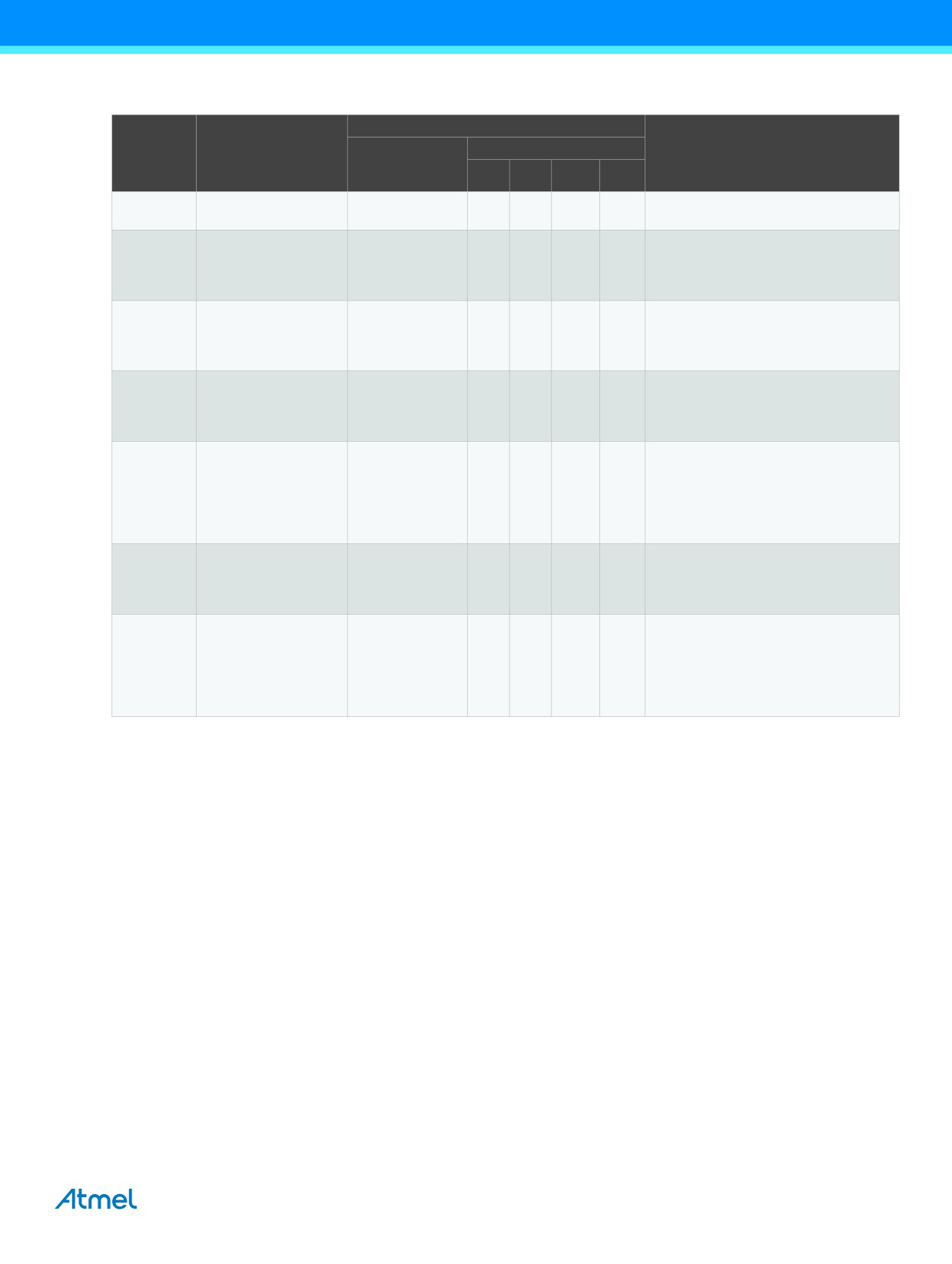
Table 21-4.
Status Codes for Master Receiver Mode
Application Software Response
Status Code
Status of the 2-wire
(TWSR)
Serial Bus and 2-wire
To/from TWDR
To TWCR
Prescaler
Serial Interface
Bits are 0
Hardware
STA
STO
TWINT
TWEA
Next Action Taken by TWI Hardware
0x08
A START condition has
Load SLA+R
0
0
1
X
SLA+R will be transmitted
been transmitted
ACK or NOT ACK will be received
0x10
A repeated START
Load SLA+R or
0
0
1
X
SLA+R will be transmitted
condition has been
ACK or NOT ACK will be received
transmitted
Load SLA+W
0
0
1
X
SLA+W will be transmitted
logic will switch to master transmitter mode
0x38
Arbitration lost in SLA+R
No TWDR action or
0
0
1
X
2-wire serial bus will be released and not
or NOT ACK bit
addressed slave mode will be entered
No TWDR action
1
0
1
X
A START condition will be transmitted when
the bus becomes free
0x40
SLA+R has been
No TWDR action or
0
0
1
0
Data byte will be received and NOT ACK
transmitted; ACK has
will be returned
been received
No TWDR action
0
0
1
1
Data byte will be received and ACK will be
returned
0x48
SLA+R has been
No TWDR action or
1
0
1
X
Repeated START will be transmitted
transmitted; NOT ACK
No TWDR action or
0
1
1
X
STOP condition will be transmitted and
has been received
TWSTO flag will be reset
No TWDR action
1
1
1
X
STOP condition followed by a START
condition will be transmitted and TWSTO
flag will be reset
0x50
Data byte has been
Read data byte or
0
0
1
0
Data byte will be received and NOT ACK
received; ACK has been
will be returned
returned
Read data byte
0
0
1
1
Data byte will be received and ACK will be
returned
0x58
Data byte has been
Read data byte or
1
0
1
X
Repeated START will be transmitted
received; NOT ACK has
Read data byte or
0
1
1
X
STOP condition will be transmitted and
been returned
TWSTO flag will be reset
Read data byte
1
1
1
X
STOP condition followed by a START
condition will be transmitted and TWSTO
flag will be reset
ATmega328P [DATASHEET]
189
7810D-AVR-01/15
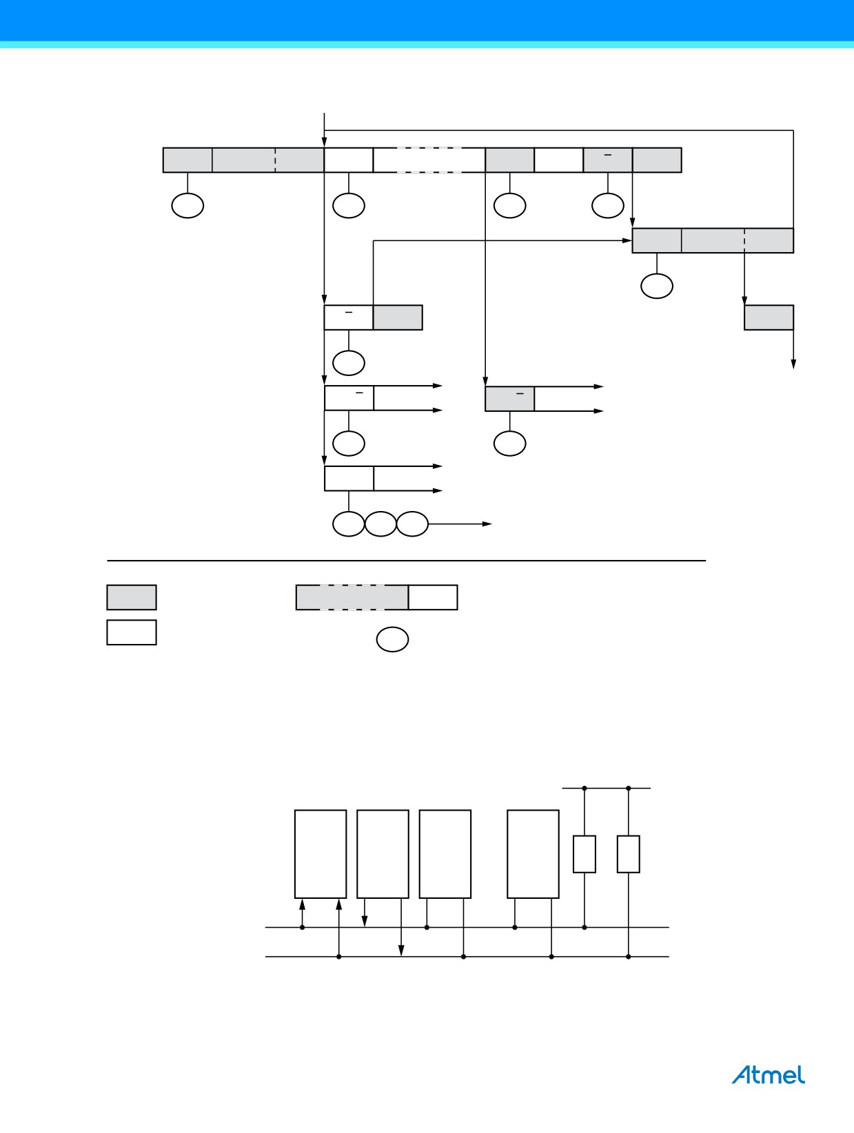
Figure 21-14. Formats and States in the Master Receiver Mode
MR
Successfull
reception
S
SLA
R
A
DATA
A
DATA
A
P
from a slave
receiver
$08
$40
$50
$58
Next transfer
started with a
RS
SLA
R
repeated start
condition
$10
Not acknowledge
received after the
A
P
W
slave address
$48
MT
Arbitration lost in slave
Other master
Other master
A or A
A or A
address or data byte
continues
continues
$38
$38
Arbitration lost and
Other master
A
addressed as slave
continues
To corresponding
$68
$78
$B0
states in slave mode
From master to slave
DATA
A
Any number of data bytes
and their associated acknowledge bits
From slave to master
This number (contained in TWSR) corresponds
n
to a defined state of the 2-Wire Serial Bus.
The prescaler bits are zero or masked to zero
21.7.3
Slave Receiver Mode
In the slave receiver mode, a number of data bytes are received from a master transmitter (see Figure 21-15). All the status
codes mentioned in this section assume that the prescaler bits are zero or are masked to zero.
Figure 21-15. Data Transfer in Slave Receiver Mode
VCC
Device 1
Device 2
Slave
Master
Device 3
Device n
R1
R2
Receiver
Transmitter
SDA
SCL
190
ATmega328P [DATASHEET]
7810D-AVR-01/15
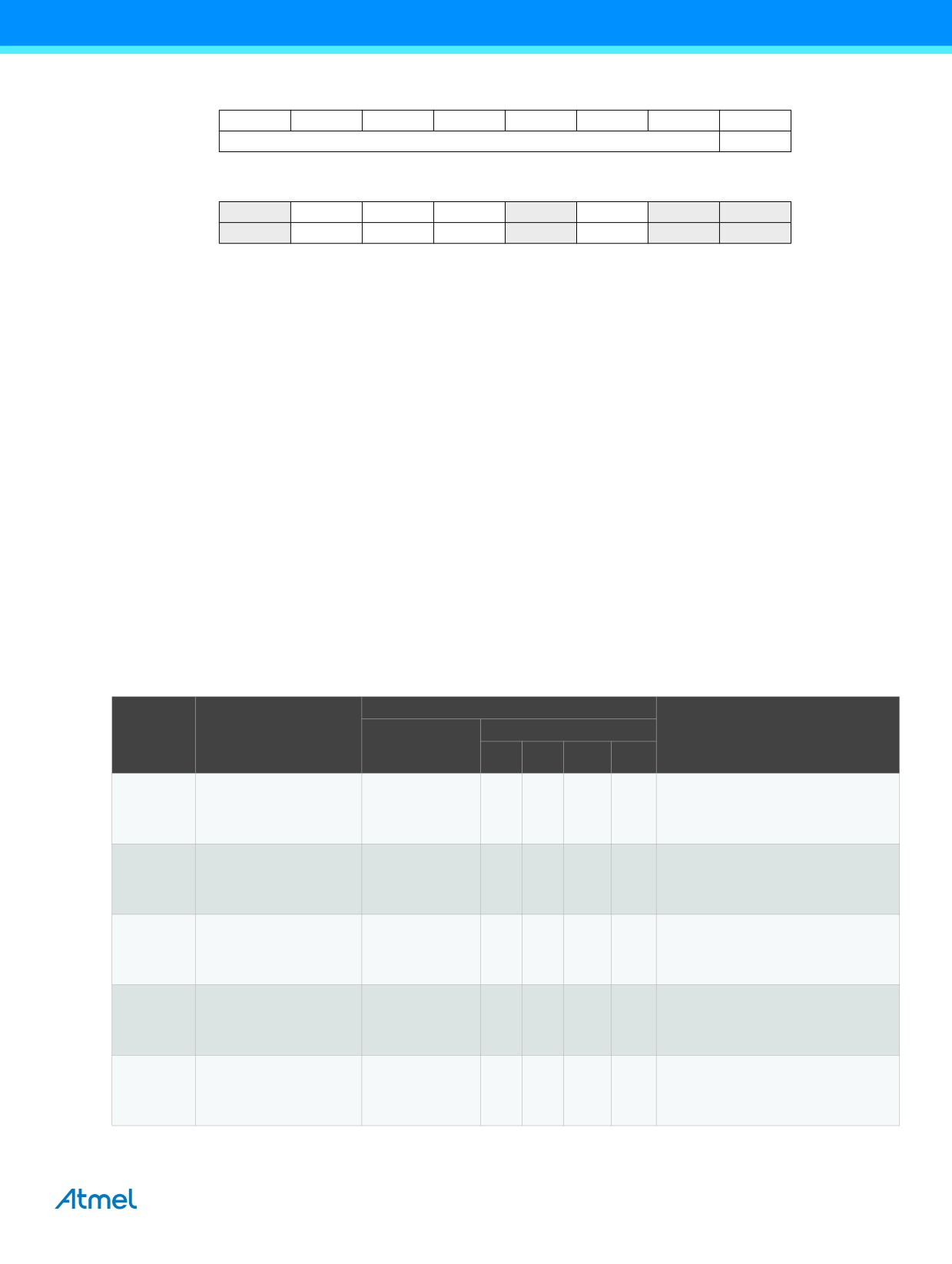
To initiate the slave receiver mode, TWAR and TWCR must be initialized as follows:
TWAR
TWA6
TWA5
TWA4
TWA3
TWA2
TWA1
TWA0
TWGCE
value
Device’s own slave address
The upper 7 bits are the address to which the 2-wire serial interface will respond when addressed by a master. If the LSB is
set, the TWI will respond to the general call address (0x00), otherwise it will ignore the general call address.
TWCR
TWINT
TWEA
TWSTA
TWSTO
TWWC
TWEN
-
TWIE
value
0
1
0
0
0
1
0
X
TWEN must be written to one to enable the TWI. The TWEA bit must be written to one to enable the acknowledgement of
the device’s own slave address or the general call address. TWSTA and TWSTO must be written to zero.
When TWAR and TWCR have been initialized, the TWI waits until it is addressed by its own slave address (or the general
call address if enabled) followed by the data direction bit. If the direction bit is “0” (write), the TWI will operate in SR mode,
otherwise ST mode is entered. After its own slave address and the write bit have been received, the TWINT flag is set and a
valid status code can be read from TWSR. The status code is used to determine the appropriate software action. The
appropriate action to be taken for each status code is detailed in Table 21-5. The slave receiver mode may also be entered if
arbitration is lost while the TWI is in the master mode (see states 0x68 and 0x78).
If the TWEA bit is reset during a transfer, the TWI will return a “not acknowledge” (“1”) to SDA after the next received data
byte. This can be used to indicate that the slave is not able to receive any more bytes. While TWEA is zero, the TWI does not
acknowledge its own slave address. However, the 2-wire serial bus is still monitored and address recognition may resume at
any time by setting TWEA. This implies that the TWEA bit may be used to temporarily isolate the TWI from the 2-wire serial
bus.
In all sleep modes other than Idle mode, the clock system to the TWI is turned off. If the TWEA bit is set, the interface can
still acknowledge its own slave address or the general call address by using the 2-wire serial bus clock as a clock source.
The part will then wake up from sleep and the TWI will hold the SCL clock low during the wake up and until the TWINT flag is
cleared (by writing it to one). Further data reception will be carried out as normal, with the AVR® clocks running as normal.
Observe that if the AVR is set up with a long start-up time, the SCL line may be held low for a long time, blocking other data
transmissions.
Note that the 2-wire serial interface data register - TWDR does not reflect the last byte present on the bus when waking up
from these sleep modes.
Table 21-5. Status Codes for Slave Receiver Mode
Application Software Response
Status Code
(TWSR)
Status of the 2-wire Serial
To/from TWDR
To TWCR
Prescaler
Bus and 2-wire Serial
Bits are 0
Interface Hardware
STA
STO
TWINT
TWEA
Next Action Taken by TWI Hardware
No TWDR action or
X
0
1
0
Data byte will be received and NOT ACK
Own SLA+W has been
will be returned
0x60
received; ACK has been
No TWDR action
X
0
1
1
Data byte will be received and ACK will be
returned
returned
Arbitration lost in SLA+R/W
No TWDR action or
X
0
1
0
Data byte will be received and NOT ACK
as Master; own SLA+W has
will be returned
0x68
been received; ACK has
No TWDR action
X
0
1
1
Data byte will be received and ACK will be
been returned
returned
No TWDR action or
X
0
1
0
Data byte will be received and NOT ACK
General call address has
will be returned
0x70
been received; ACK has
No TWDR action
X
0
1
1
Data byte will be received and ACK will be
been returned
returned
Arbitration lost in SLA+R/W
No TWDR action or
X
0
1
0
Data byte will be received and NOT ACK
as Master; General call
will be returned
0x78
address has been received;
No TWDR action
X
0
1
1
Data byte will be received and ACK will be
ACK has been returned
returned
Previously addressed with
Read data byte or
X
0
1
0
Data byte will be received and NOT ACK
own SLA+W; data has been
will be returned
0x80
received; ACK has been
Read data byte
X
0
1
1
Data byte will be received and ACK will be
returned
returned
ATmega328P [DATASHEET]
191
7810D-AVR-01/15
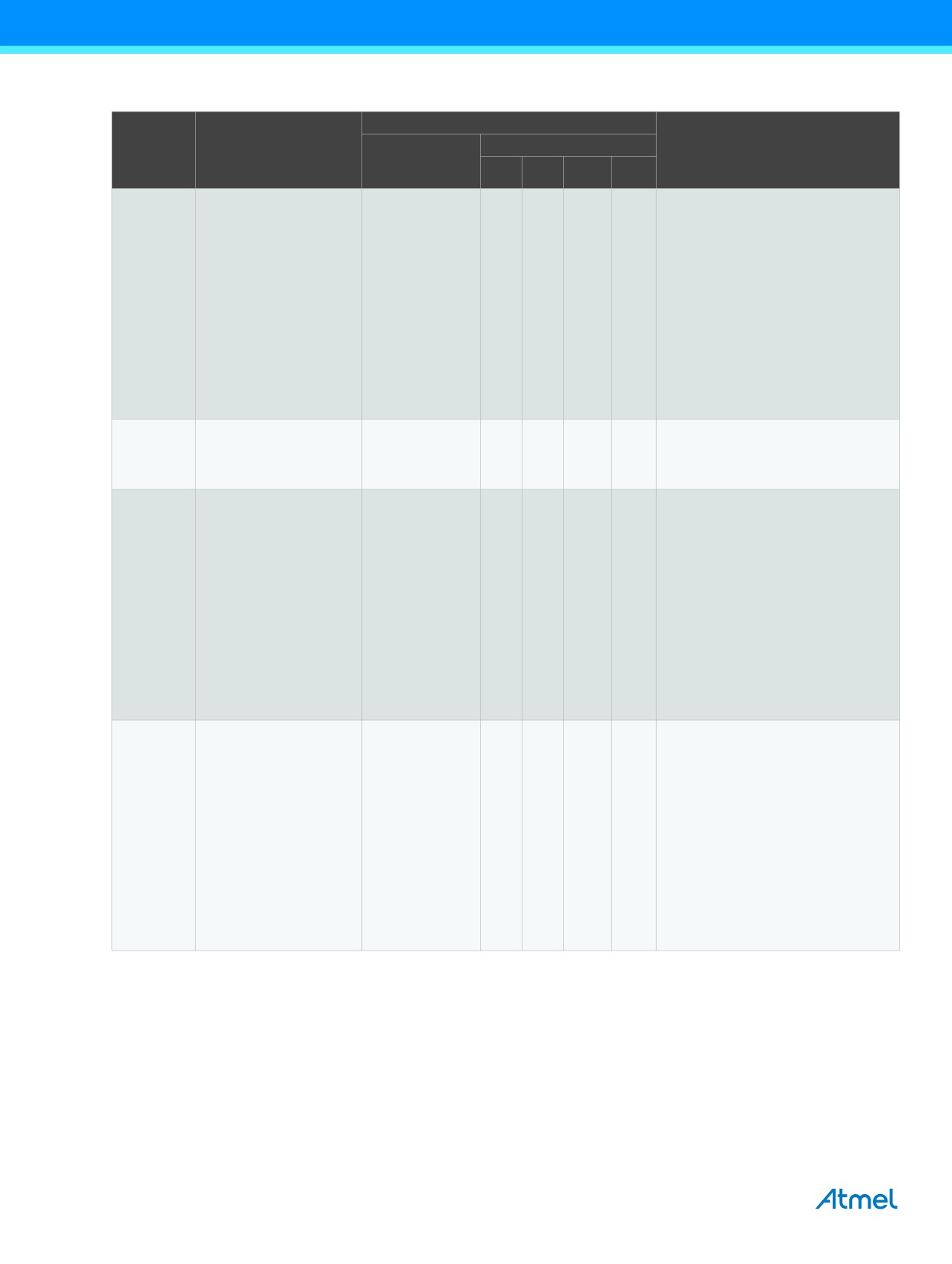
Table 21-5.
Status Codes for Slave Receiver Mode (Continued)
Application Software Response
Status Code
(TWSR)
Status of the 2-wire Serial
To/from TWDR
To TWCR
Prescaler
Bus and 2-wire Serial
Bits are 0
Interface Hardware
STA
STO
TWINT
TWEA
Next Action Taken by TWI Hardware
0x88
Previously addressed with
Read data byte or
0
0
1
0
Switched to the not addressed Slave
own SLA+W; data has been
mode; no recognition of own SLA or GCA
received; NOT ACK has
Read data byte or
0
0
1
1
Switched to the not addressed Slave
been returned
mode; own SLA will be recognized; GCA
will be recognized if TWGCE = “1”
Read data byte or
1
0
1
0
Switched to the not addressed Slave
mode; no recognition of own SLA or GCA;
a START condition will be transmitted
when the bus becomes free
Read data byte
1
0
1
1
Switched to the not addressed Slave
mode; own SLA will be recognized; GCA
will be recognized if TWGCE = “1”; a
START condition will be transmitted when
the bus becomes free
0x90
Previously addressed with
Read data byte or
X
0
1
0
Data byte will be received and NOT ACK
general call; data has been
will be returned
received; ACK has been
Read data byte
X
0
1
1
Data byte will be received and ACK will be
returned
returned
0x98
Previously addressed with
Read data byte or
0
0
1
0
Switched to the not addressed Slave
general call; data has been
mode; no recognition of own SLA or GCA
received; NOT ACK has
Read data byte or
0
0
1
1
Switched to the not addressed Slave
been returned
mode; own SLA will be recognized; GCA
will be recognized if TWGCE = “1”
Read data byte or
1
0
1
0
Switched to the not addressed Slave
mode; no recognition of own SLA or GCA;
a START condition will be transmitted
when the bus becomes free
Read data byte
1
0
1
1
Switched to the not addressed Slave
mode; own SLA will be recognized; GCA
will be recognized if TWGCE = “1”; a
START condition will be transmitted when
the bus becomes free
0xA0
A STOP condition or
No action
0
0
1
0
Switched to the not addressed Slave
repeated START condition
mode; no recognition of own SLA or GCA
has been received while still
0
0
1
1
Switched to the not addressed Slave
addressed as slave
mode; own SLA will be recognized; GCA
will be recognized if TWGCE = “1”
1
0
1
0
Switched to the not addressed Slave
mode; no recognition of own SLA or GCA;
a START condition will be transmitted
when the bus becomes free
1
0
1
1
Switched to the not addressed Slave
mode; own SLA will be recognized; GCA
will be recognized if TWGCE = “1”; a
START condition will be transmitted when
the bus becomes free
192
ATmega328P [DATASHEET]
7810D-AVR-01/15
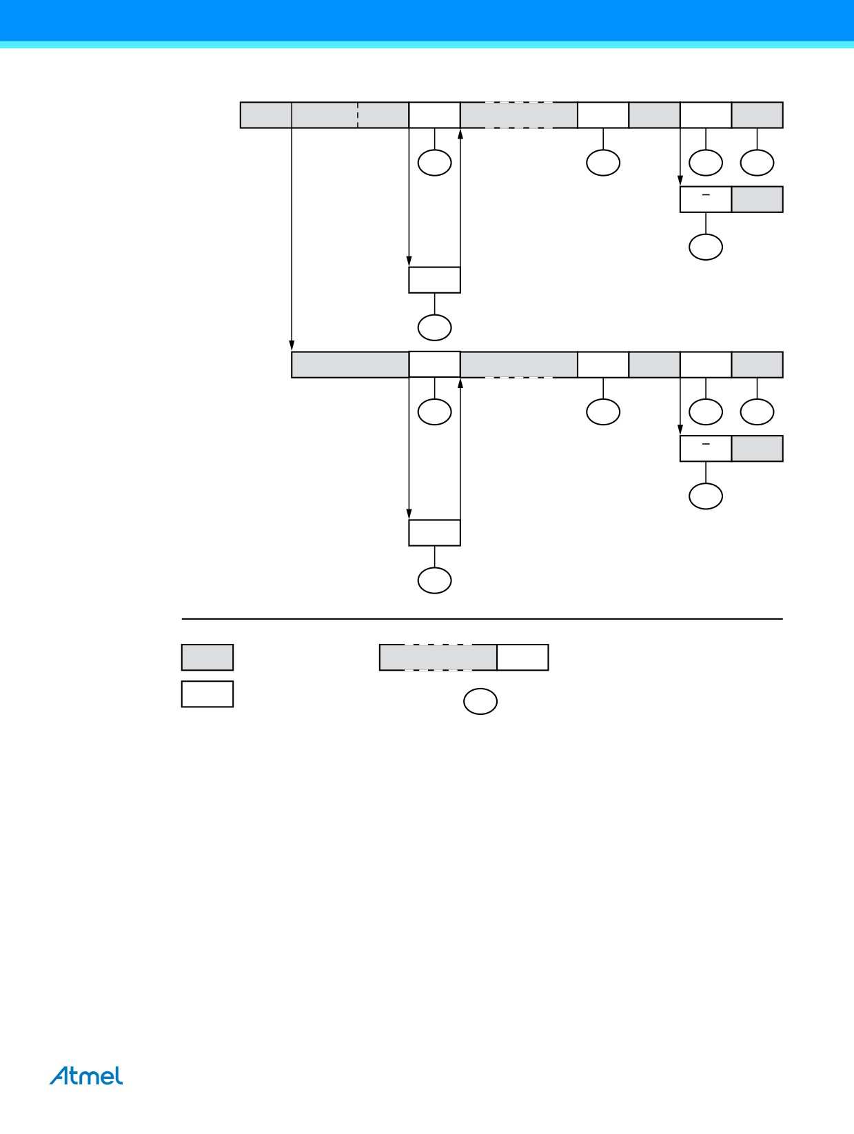
Figure 21-16. Formats and States in the Slave Receiver Mode
Reception of the own
slave address and one or
S
SLA
W
A
DATA
A
DATA
A
P or S
more data bytes. All are
acknowledged
$60
$80
$80
$A0
Last data byte received
is not acknowledged
A
P or S
$88
Arbitration lost as master
and addressed as slave
A
Reception of the general call
$68
address and one or more
data bytes
General Call
A
DATA
A
DATA
A
P or S
$70
$90
$90
$A0
Last data byte received
A
P or S
is not acknowledged
$98
Arbitration lost as master
A
and as slave by general call
$78
Any number of data bytes
From master to slave
DATA
A
and their associated acknowledge bits
From slave to master
This number (contained in TWSR) corresponds
n
to a defined state of the 2-Wire Serial Bus.
The prescaler bits are zero or masked to zero
ATmega328P [DATASHEET]
193
7810D-AVR-01/15
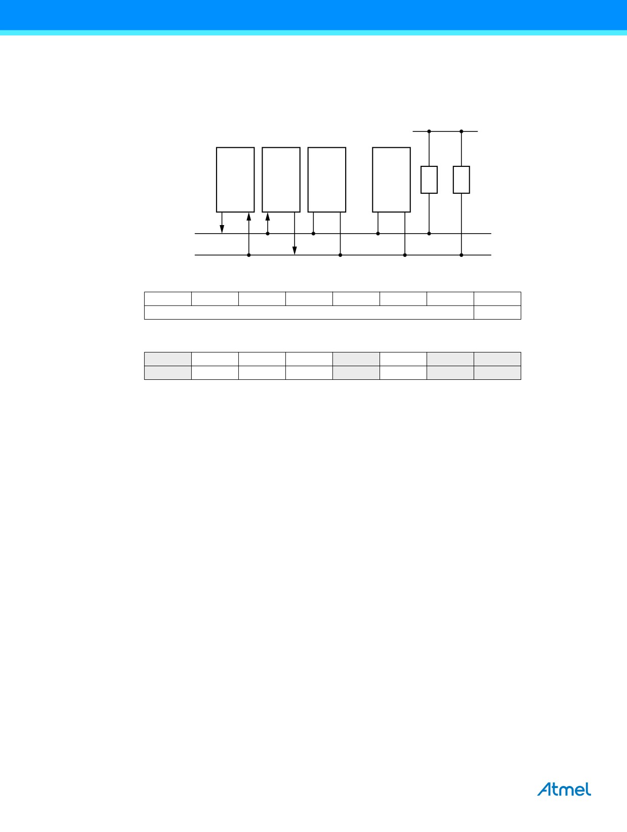
21.7.4
Slave Transmitter Mode
In the slave transmitter mode, a number of data bytes are transmitted to a master receiver (see Figure 21-17). All the status
codes mentioned in this section assume that the prescaler bits are zero or are masked to zero.
Figure 21-17. Data Transfer in Slave Transmitter Mode
VCC
Device 1
Device 2
Slave
Master
Device 3
Device n
R1
R2
Transmitter
Receiver
SDA
SCL
To initiate the slave transmitter mode, TWAR and TWCR must be initialized as follows:
TWAR
TWA6
TWA5
TWA4
TWA3
TWA2
TWA1
TWA0
TWGCE
value
Device’s Own Slave Address
The upper seven bits are the address to which the 2-wire serial interface will respond when addressed by a master. If the
LSB is set, the TWI will respond to the general call address (0x00), otherwise it will ignore the general call address.
TWCR
TWINT
TWEA
TWSTA
TWSTO
TWWC
TWEN
-
TWIE
value
0
1
0
0
0
1
0
X
TWEN must be written to one to enable the TWI. The TWEA bit must be written to one to enable the acknowledgement of
the device’s own slave address or the general call address. TWSTA and TWSTO must be written to zero.
When TWAR and TWCR have been initialized, the TWI waits until it is addressed by its own slave address (or the general
call address if enabled) followed by the data direction bit. If the direction bit is “1” (read), the TWI will operate in ST mode,
otherwise SR mode is entered. After its own slave address and the write bit have been received, the TWINT flag is set and a
valid status code can be read from TWSR. The status code is used to determine the appropriate software action. The
appropriate action to be taken for each status code is detailed in Table 21-6 on page 195. The slave transmitter mode may
also be entered if arbitration is lost while the TWI is in the master mode (see state 0xB0).
If the TWEA bit is written to zero during a transfer, the TWI will transmit the last byte of the transfer. State 0xC0 or state 0xC8
will be entered, depending on whether the master receiver transmits a NACK or ACK after the final byte. The TWI is
switched to the not addressed slave mode, and will ignore the master if it continues the transfer. Thus the master receiver
receives all “1” as serial data. State 0xC8 is entered if the master demands additional data bytes (by transmitting ACK), even
though the slave has transmitted the last byte (TWEA zero and expecting NACK from the master).
While TWEA is zero, the TWI does not respond to its own slave address. However, the 2-wire serial bus is still monitored
and address recognition may resume at any time by setting TWEA. This implies that the TWEA bit may be used to
temporarily isolate the TWI from the 2-wire serial bus.
In all sleep modes other than idle mode, the clock system to the TWI is turned off. If the TWEA bit is set, the interface can still
acknowledge its own slave address or the general call address by using the 2-wire serial bus clock as a clock source. The
part will then wake up from sleep and the TWI will hold the SCL clock will low during the wake up and until the TWINT flag is
cleared (by writing it to one). Further data transmission will be carried out as normal, with the AVR® clocks running as
normal. Observe that if the AVR is set up with a long start-up time, the SCL line may be held low for a long time, blocking
other data transmissions.
Note that the 2-wire serial interface data register - TWDR does not reflect the last byte present on the bus when waking up
from these sleep modes.
194
ATmega328P [DATASHEET]
7810D-AVR-01/15
Table 21-6.
Status Codes for Slave Transmitter Mode
Application Software Response
Status Code
(TWSR)
Status of the 2-wire Serial
To/from TWDR
To TWCR
Prescaler
Bus and 2-wire Serial
Bits are 0
Interface Hardware
STA
STO
TWINT
TWEA
Next Action Taken by TWI Hardware
0xA8
Own SLA+R has been
Load data byte or
X
0
1
0
Last data byte will be transmitted and
received; ACK has been
NOT ACK should be received
returned
Load data byte
X
0
1
1
Data byte will be transmitted and ACK
should be received
0xB0
Arbitration lost in SLA+R/W
Load data byte or
X
0
1
0
Last data byte will be transmitted and
as Master; own SLA+R has
NOT ACK should be received
been received; ACK has
Load data byte
X
0
1
1
Data byte will be transmitted and ACK
been returned
should be received
0xB8
Data byte in TWDR has
Load data byte or
X
0
1
0
Last data byte will be transmitted and
been transmitted; ACK has
NOT ACK should be received
been received
Load data byte
X
0
1
1
Data byte will be transmitted and ACK
should be received
0xC0
Data byte in TWDR has
No TWDR action or
0
0
1
0
Switched to the not addressed Slave
been transmitted; NOT
mode; no recognition of own SLA or GCA
ACK has been received
No TWDR action or
0
0
1
1
Switched to the not addressed slave
mode; own SLA will be recognized; GCA
will be recognized if TWGCE = “1”
No TWDR action or
1
0
1
0
Switched to the not addressed Slave
mode; no recognition of own SLA or
GCA; a START condition will be
transmitted when the bus becomes free
No TWDR action
1
0
1
1
Switched to the not addressed Slave
mode; own SLA will be recognized; GCA
will be recognized if TWGCE = “1”; a
START condition will be transmitted when
the bus becomes free
0xC8
Last data byte in TWDR
No TWDR action or
0
0
1
0
Switched to the not addressed slave
has been transmitted
mode; no recognition of own SLA or GCA
(TWEA = “0”); ACK has
No TWDR action or
0
0
1
1
Switched to the not addressed Slave
been received
mode; own SLA will be recognized; GCA
will be recognized if TWGCE = “1”
No TWDR action or
1
0
1
0
Switched to the not addressed Slave
mode; no recognition of own SLA or
GCA; a START condition will be
transmitted when the bus becomes free
No TWDR action
1
0
1
1
Switched to the not addressed Slave
mode; own SLA will be recognized; GCA
will be recognized if TWGCE = “1”; a
START condition will be transmitted when
the bus becomes free
ATmega328P [DATASHEET]
195
7810D-AVR-01/15
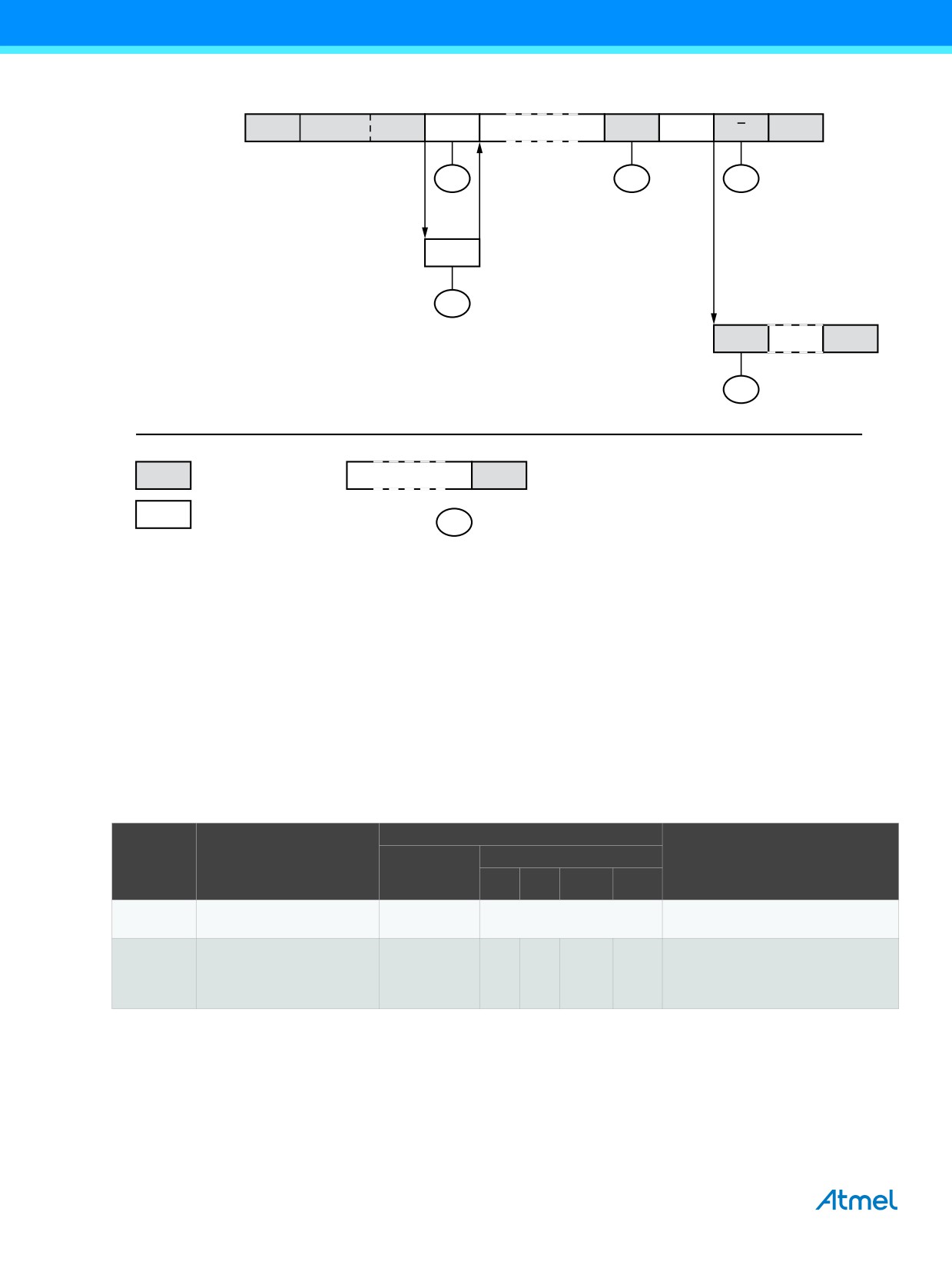
Figure 21-18. Formats and States in the Slave Transmitter Mode
Reception of the own
slave address and one
S
SLA
R
A
DATA
A
DATA
A
P or S
or more data bytes
$A8
$B8
$C0
Arbitration lost as master
A
and addressed as slave
$B0
Last data byte transmitted.
A
All 1’s
P or S
Switched to not adressed
slave (TWEA = “0”
$C8
From master to slave
DATA
A
Any number of data bytes
and their associated acknowledge bits
From slave to master
This number (contained in TWSR) corresponds
n
to a defined state of the 2-Wire Serial Bus.
The prescaler bits are zero or masked to zero
21.7.5
Miscellaneous States
There are two status codes that do not correspond to a defined TWI state, see Table 21-7.
Status 0xF8 indicates that no relevant information is available because the TWINT flag is not set. This occurs between other
states, and when the TWI is not involved in a serial transfer.
Status 0x00 indicates that a bus error has occurred during a 2-wire serial bus transfer. A bus error occurs when a START or
STOP condition occurs at an illegal position in the format frame. Examples of such illegal positions are during the serial
transfer of an address byte, a data byte, or an acknowledge bit. When a bus error occurs, TWINT is set. To recover from a
bus error, the TWSTO flag must set and TWINT must be cleared by writing a logic one to it. This causes the TWI to enter the
not addressed slave mode and to clear the TWSTO flag (no other bits in TWCR are affected). The SDA and SCL lines are
released, and no STOP condition is transmitted.
Table 21-7. Miscellaneous States
Application Software Response
Status Code
(TWSR)
Status of the 2-wire Serial
To/from TWDR
To TWCR
Prescaler
Bus and 2-wire Serial
Bits are 0
Interface Hardware
STA
STO
TWINT
TWEA
Next Action Taken by TWI Hardware
No relevant state information
No TWDR
0xF8
No TWCR action
Wait or proceed current transfer
available; TWINT = “0”
action
Only the internal hardware is affected,
Bus error due to an illegal
No TWDR
no STOP condition is sent on the bus. In
0x00
0
1
1
X
START or STOP condition
action
all cases, the bus is released and
TWSTO is cleared.
196
ATmega328P [DATASHEET]
7810D-AVR-01/15
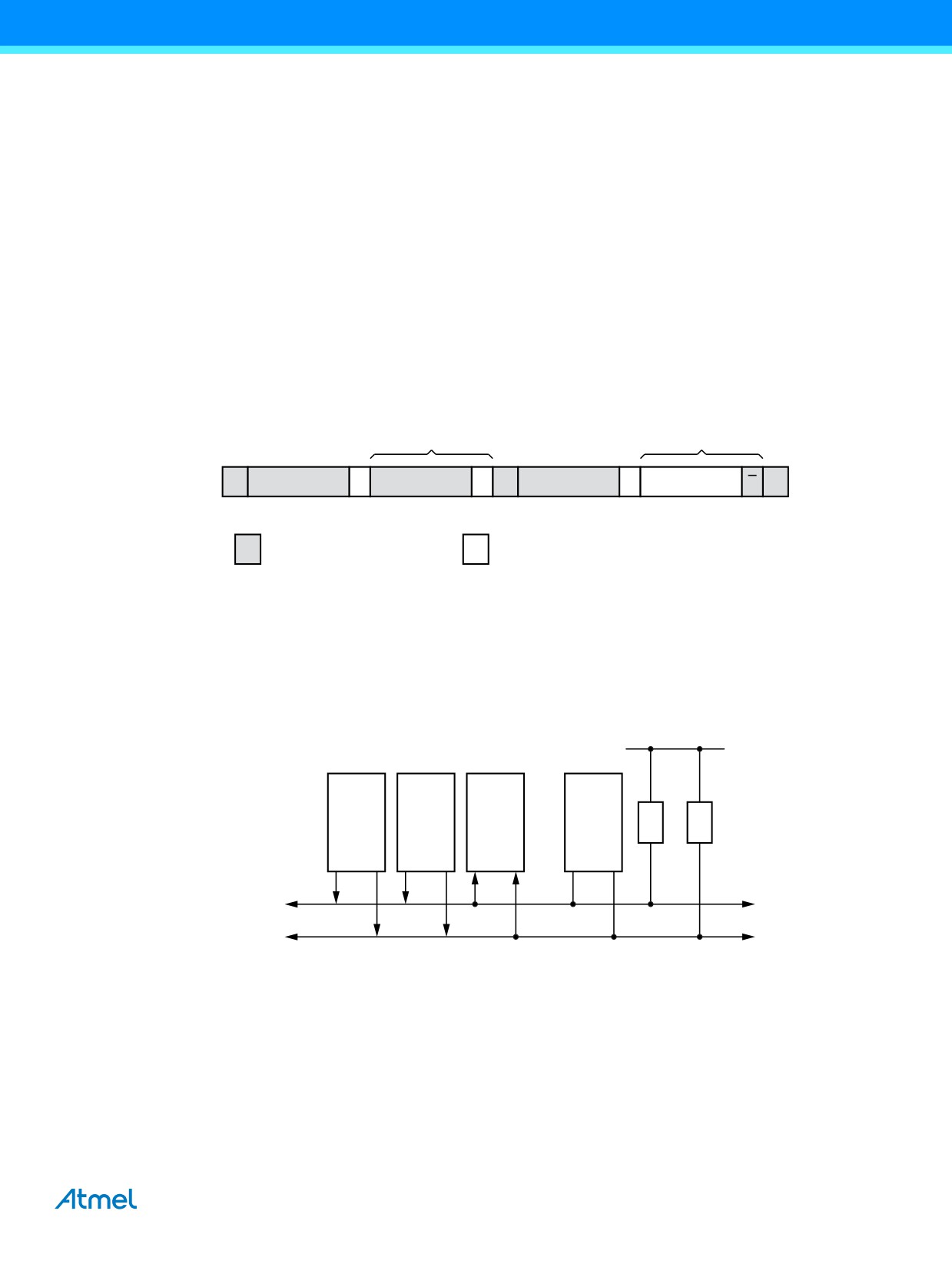
21.7.6
Combining Several TWI Modes
In some cases, several TWI modes must be combined in order to complete the desired action. Consider for example reading
data from a serial EEPROM. Typically, such a transfer involves the following steps:
1.
The transfer must be initiated.
2.
The EEPROM must be instructed what location should be read.
3.
The reading must be performed.
4.
The transfer must be finished.
Note that data is transmitted both from master to slave and vice versa. The master must instruct the slave what location it
wants to read, requiring the use of the MT mode. Subsequently, data must be read from the slave, implying the use of the
MR mode. Thus, the transfer direction must be changed. The master must keep control of the bus during all these steps, and
the steps should be carried out as an atomical operation. If this principle is violated in a multi master system, another Master
can alter the data pointer in the EEPROM between steps 2 and 3, and the master will read the wrong data location. Such a
change in transfer direction is accomplished by transmitting a REPEATED START between the transmission of the address
byte and reception of the data. After a REPEATED START, the master keeps ownership of the bus. The following figure
shows the flow in this transfer.
Figure 21-19. Combining Several TWI Modes to Access a Serial EEPROM
Master Transmitter
Master Receiver
S
SLA + W
A
ADDRESS
A
RS
SLA + R
A
DATA
A
P
S = START
R
S = REPEATED START
P = STOP
Transmitted from master to slave
Transmitted from slave to master
21.8
Multi-master Systems and Arbitration
If multiple masters are connected to the same bus, transmissions may be initiated simultaneously by one or more of them.
The TWI standard ensures that such situations are handled in such a way that one of the masters will be allowed to proceed
with the transfer, and that no data will be lost in the process. An example of an arbitration situation is depicted below, where
two masters are trying to transmit data to a slave receiver.
Figure 21-20. An Arbitration Example
VCC
Device 1
Device 2
Device 3
Master
Master
Slave
Device n
R1
R2
Transmitter
Transmitter
Receiver
SDA
SCL
ATmega328P [DATASHEET]
197
7810D-AVR-01/15
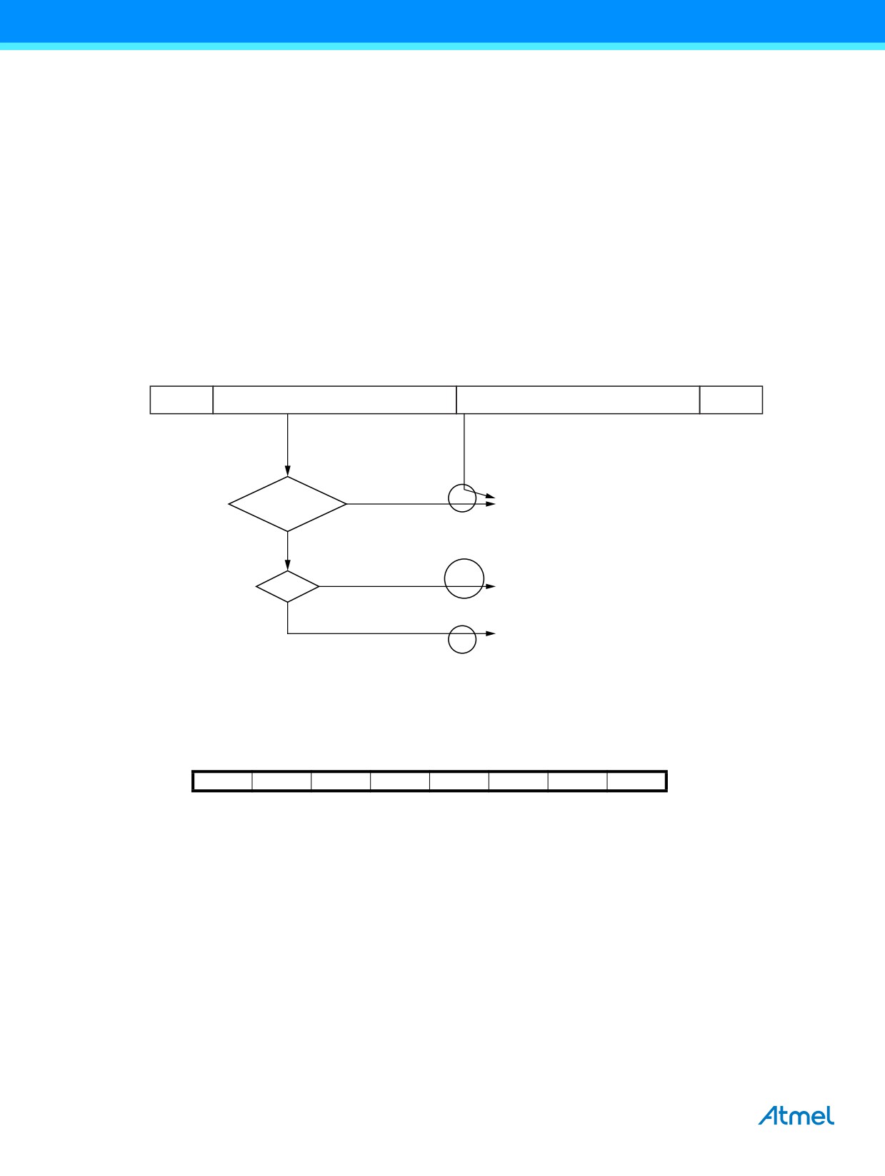
Several different scenarios may arise during arbitration, as described below:
● Two or more masters are performing identical communication with the same slave. In this case, neither the slave nor
any of the masters will know about the bus contention.
● Two or more masters are accessing the same slave with different data or direction bit. In this case, arbitration will
occur, either in the READ/WRITE bit or in the data bits. The masters trying to output a one on SDA while another
Master outputs a zero will lose the arbitration. Losing masters will switch to not addressed Slave mode or wait until the
bus is free and transmit a new START condition, depending on application software action.
● Two or more masters are accessing different slaves. In this case, arbitration will occur in the SLA bits. Masters trying
to output a one on SDA while another master outputs a zero will lose the arbitration. Masters losing arbitration in SLA
will switch to slave mode to check if they are being addressed by the winning master. If addressed, they will switch to
SR or ST mode, depending on the value of the READ/WRITE bit. If they are not being addressed, they will switch to
not addressed slave mode or wait until the bus is free and transmit a new START condition, depending on application
software action.
This is summarized in Figure 21-21. Possible status values are given in circles.
Figure 21-21. Possible Status Codes Caused by Arbitration
START
SLA
DATA
STOP
Arbitration lost in SLA
Arbitration lost in DATA
Own
NO
38
TWI bus will be released and not addressed slave mode will be entered
Address/ General Call
A START condition will be transmitted when the bus becomes free
received
YES
68/78
Write
Data byte will be received and NOT ACK will be returned
Direction
Data byte will be received and ACK will be returned
Read
Last data byte will be transmitted and NOT ACK should be received
B0
Data byte will be transmitted and ACK should be received
21.9
Register Description
21.9.1
TWBR - TWI Bit Rate Register
Bit
7
6
5
4
3
2
1
0
(0xB8)
TWBR7
TWBR6
TWBR5
TWBR4
TWBR3
TWBR2
TWBR1
TWBR0
TWBR
Read/Write
R/W
R/W
R/W
R/W
R/W
R/W
R/W
R/W
Initial Value
0
0
0
0
0
0
0
0
• Bits 7..0 - TWI Bit Rate Register
TWBR selects the division factor for the bit rate generator. The bit rate generator is a frequency divider which generates the
SCL clock frequency in the master modes. See Section 21.5.2 “Bit Rate Generator Unit” on page 180 for calculating bit
rates.
198
ATmega328P [DATASHEET]
7810D-AVR-01/15
21.9.2
TWCR - TWI Control Register
Bit
7
6
5
4
3
2
1
0
(0xBC)
TWINT
TWEA
TWSTA
TWSTO
TWWC
TWEN
-
TWIE
TWCR
Read/Write
R/W
R/W
R/W
R/W
R
R/W
R
R/W
Initial Value
0
0
0
0
0
0
0
0
The TWCR is used to control the operation of the TWI. It is used to enable the TWI, to initiate a master access by applying a
START condition to the bus, to generate a receiver acknowledge, to generate a stop condition, and to control halting of the
bus while the data to be written to the bus are written to the TWDR. It also indicates a write collision if data is attempted
written to TWDR while the register is inaccessible.
• Bit 7 - TWINT: TWI Interrupt Flag
This bit is set by hardware when the TWI has finished its current job and expects application software response. If the I-bit in
SREG and TWIE in TWCR are set, the MCU will jump to the TWI interrupt vector. While the TWINT flag is set, the SCL low
period is stretched. The TWINT flag must be cleared by software by writing a logic one to it. Note that this flag is not
automatically cleared by hardware when executing the interrupt routine. Also note that clearing this flag starts the operation
of the TWI, so all accesses to the TWI address register (TWAR), TWI status register (TWSR), and TWI data register (TWDR)
must be complete before clearing this flag.
• Bit 6 - TWEA: TWI Enable Acknowledge Bit
The TWEA bit controls the generation of the acknowledge pulse. If the TWEA bit is written to one, the ACK pulse is
generated on the TWI bus if the following conditions are met:
1.
The device’s own slave address has been received.
2.
A general call has been received, while the TWGCE bit in the TWAR is set.
3.
A data byte has been received in master receiver or slave receiver mode.
By writing the TWEA bit to zero, the device can be virtually disconnected from the 2-wire serial bus temporarily. Address
recognition can then be resumed by writing the TWEA bit to one again.
• Bit 5 - TWSTA: TWI START Condition Bit
The application writes the TWSTA bit to one when it desires to become a master on the 2-wire serial bus. The TWI hardware
checks if the bus is available, and generates a START condition on the bus if it is free. However, if the bus is not free, the
TWI waits until a STOP condition is detected, and then generates a new START condition to claim the bus master status.
TWSTA must be cleared by software when the START condition has been transmitted.
• Bit 4 - TWSTO: TWI STOP Condition Bit
Writing the TWSTO bit to one in master mode will generate a STOP condition on the 2-wire serial bus. When the STOP
condition is executed on the bus, the TWSTO bit is cleared automatically. In slave mode, setting the TWSTO bit can be used
to recover from an error condition. This will not generate a STOP condition, but the TWI returns to a well-defined
unaddressed slave mode and releases the SCL and SDA lines to a high impedance state.
• Bit 3 - TWWC: TWI Write Collision Flag
The TWWC bit is set when attempting to write to the TWI data register - TWDR when TWINT is low. This flag is cleared by
writing the TWDR register when TWINT is high.
• Bit 2 - TWEN: TWI Enable Bit
The TWEN bit enables TWI operation and activates the TWI interface. When TWEN is written to one, the TWI takes control
over the I/O pins connected to the SCL and SDA pins, enabling the slew-rate limiters and spike filters. If this bit is written to
zero, the TWI is switched off and all TWI transmissions are terminated, regardless of any ongoing operation.
• Bit 1 - Res: Reserved Bit
This bit is a reserved bit and will always read as zero.
• Bit 0 - TWIE: TWI Interrupt Enable
When this bit is written to one, and the I-bit in SREG is set, the TWI interrupt request will be activated for as long as the
TWINT flag is high.
ATmega328P [DATASHEET]
199
7810D-AVR-01/15