Atmel ATmega328P 8-bit AVR Microcontroller. DATASHEET (2015) - page 3
14.7.3
Fast PWM Mode
The fast pulse width modulation or fast PWM mode (WGM02:0 = 3 or 7) provides a high frequency PWM waveform
generation option. The fast PWM differs from the other PWM option by its single-slope operation. The counter counts from
BOTTOM to TOP then restarts from BOTTOM. TOP is defined as 0xFF when WGM2:0 = 3, and OCR0A when WGM2:0 = 7.
In non-inverting compare output mode, the output compare (OC0x) is cleared on the compare match between TCNT0 and
OCR0x, and set at BOTTOM. In inverting compare output mode, the output is set on compare match and cleared at
BOTTOM. Due to the single-slope operation, the operating frequency of the fast PWM mode can be twice as high as the
phase correct PWM mode that use dual-slope operation. This high frequency makes the fast PWM mode well suited for
power regulation, rectification, and DAC applications. High frequency allows physically small sized external components
(coils, capacitors), and therefore reduces total system cost.
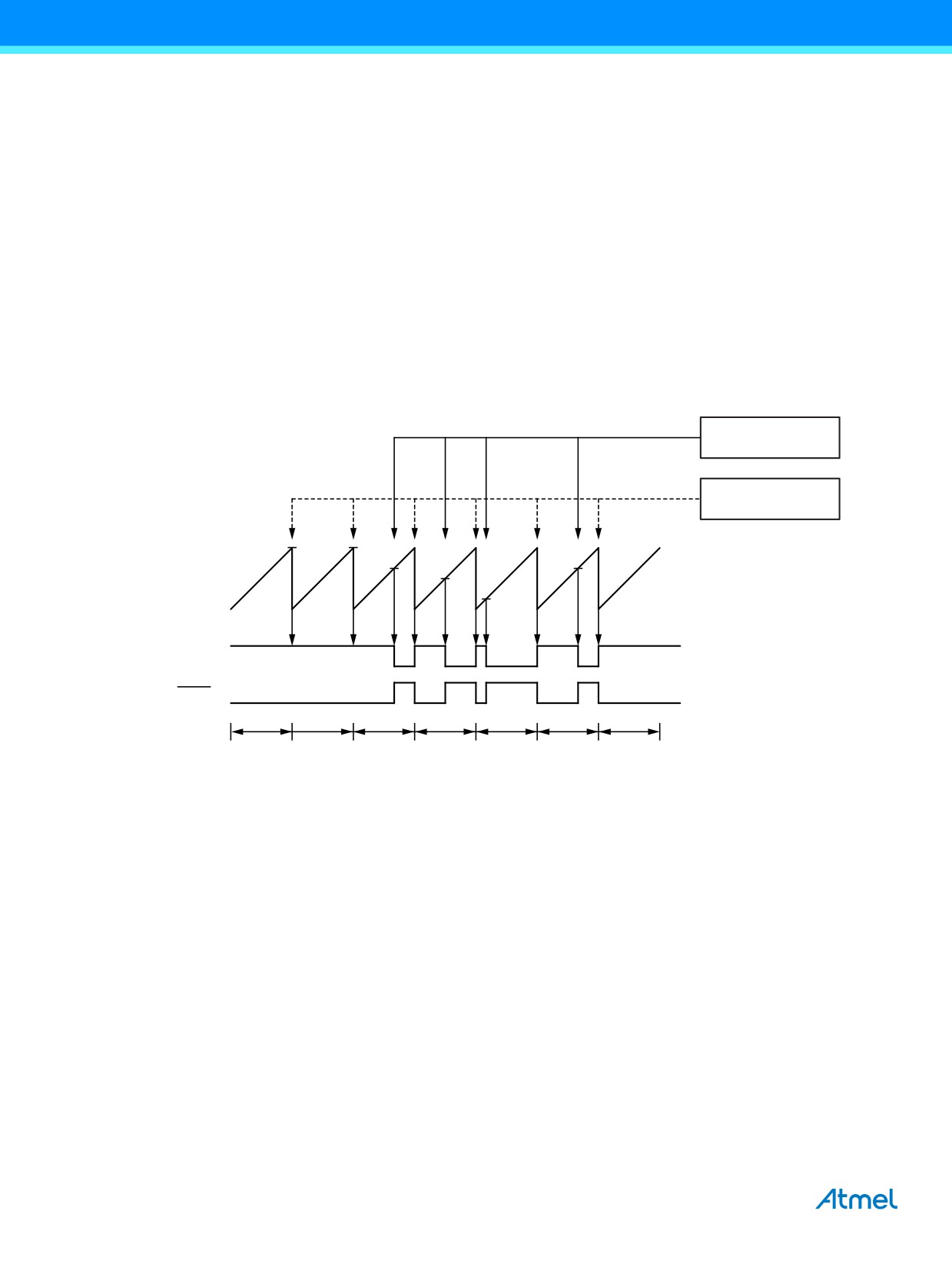
In fast PWM mode, the counter is incremented until the counter value matches the TOP value. The counter is then cleared at
the following timer clock cycle. The timing diagram for the fast PWM mode is shown in Figure 14-6. The TCNT0 value is in
the timing diagram shown as a histogram for illustrating the single-slope operation. The diagram includes non-inverted and
inverted PWM outputs. The small horizontal line marks on the TCNT0 slopes represent compare matches between OCR0x
and TCNT0.
Figure 14-6. Fast PWM Mode, Timing Diagram
OCRnx Interrupt
Flag Set
OCRnx Update and
TOVn Interrupt Flag Set
TCNTn
OCnx
(COMnx1:0 = 2)
OCnx
(COMnx1:0 = 3)
1
2
3
4
5
6
7
Period
The Timer/Counter overflow flag (TOV0) is set each time the counter reaches TOP. If the interrupt is enabled, the interrupt
handler routine can be used for updating the compare value.
In fast PWM mode, the compare unit allows generation of PWM waveforms on the OC0x pins. Setting the COM0x1:0 bits to
two will produce a non-inverted PWM and an inverted PWM output can be generated by setting the COM0x1:0 to three:
Setting the COM0A1:0 bits to one allows the OC0A pin to toggle on compare matches if the WGM02 bit is set. This option is
not available for the OC0B pin (see Table 14-6 on page 85). The actual OC0x value will only be visible on the port pin if the
data direction for the port pin is set as output. The PWM waveform is generated by setting (or clearing) the OC0x register at
the compare match between OCR0x and TCNT0, and clearing (or setting) the OC0x register at the timer clock cycle the
counter is cleared (changes from TOP to BOTTOM).
The PWM frequency for the output can be calculated by the following equation:
fclk_I/O
fOCnxPWM
= -------------------
N 256
The N variable represents the prescale factor (1, 8, 64, 256, or 1024).
80
ATmega328P [DATASHEET]
7810D-AVR-01/15
The extreme values for the OCR0A register represents special cases when generating a PWM waveform output in the fast
PWM mode. If the OCR0A is set equal to BOTTOM, the output will be a narrow spike for each MAX+1 timer clock cycle.
Setting the OCR0A equal to MAX will result in a constantly high or low output (depending on the polarity of the output set by
the COM0A1:0 bits.)
A frequency (with 50% duty cycle) waveform output in fast PWM mode can be achieved by setting OC0x to toggle its logical
level on each compare match (COM0x1:0 = 1). The waveform generated will have a maximum frequency of fOC0 = fclk_I/O/2
when OCR0A is set to zero. This feature is similar to the OC0A toggle in CTC mode, except the double buffer feature of the
output compare unit is enabled in the fast PWM mode.
14.7.4
Phase Correct PWM Mode
The phase correct PWM mode (WGM02:0 = 1 or 5) provides a high resolution phase correct PWM waveform generation
option. The phase correct PWM mode is based on a dual-slope operation. The counter counts repeatedly from BOTTOM to
TOP and then from TOP to BOTTOM. TOP is defined as 0xFF when WGM2:0 = 1, and OCR0A when WGM2:0 = 5.
In non-inverting compare output mode, the output compare (OC0x) is cleared on the compare match between TCNT0 and
OCR0x while upcounting, and set on the compare match while downcounting. In inverting output compare mode, the
operation is inverted. The dual-slope operation has lower maximum operation frequency than single slope operation.
However, due to the symmetric feature of the dual-slope PWM modes, these modes are preferred for motor control
applications.
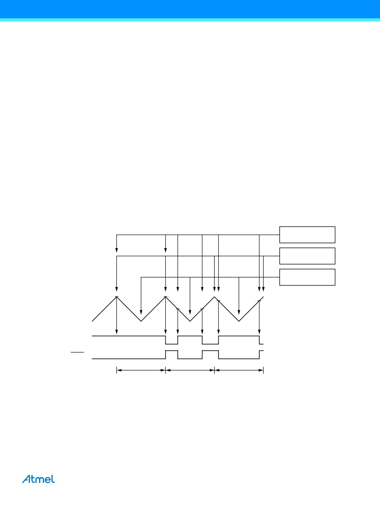
In phase correct PWM mode the counter is incremented until the counter value matches TOP. When the counter reaches
TOP, it changes the count direction. The TCNT0 value will be equal to TOP for one timer clock cycle. The timing diagram for
the phase correct PWM mode is shown on Figure 14-7. The TCNT0 value is in the timing diagram shown as a histogram for
illustrating the dual-slope operation. The diagram includes non-inverted and inverted PWM outputs. The small horizontal line
marks on the TCNT0 slopes represent compare matches between OCR0x and TCNT0.
Figure 14-7. Phase Correct PWM Mode, Timing Diagram
OCnx Interrupt
Flag Set
OCRnx Update
TOVn Interrupt
Flag Set
TCNTn
(COMnx1:0 = 2)
OCnx
OCnx
(COMnx1:0 = 3)
1
2
3
Period
The Timer/Counter overflow flag (TOV0) is set each time the counter reaches BOTTOM. The interrupt flag can be used to
generate an interrupt each time the counter reaches the BOTTOM value.
ATmega328P [DATASHEET]
81
7810D-AVR-01/15
In phase correct PWM mode, the compare unit allows generation of PWM waveforms on the OC0x pins. Setting the
COM0x1:0 bits to two will produce a non-inverted PWM. An inverted PWM output can be generated by setting the
COM0x1:0 to three: Setting the COM0A0 bits to one allows the OC0A pin to toggle on compare matches if the WGM02 bit is
set. This option is not available for the OC0B pin (see Table 14-7 on page 85). The actual OC0x value will only be visible on
the port pin if the data direction for the port pin is set as output. The PWM waveform is generated by clearing (or setting) the
OC0x register at the compare match between OCR0x and TCNT0 when the counter increments, and setting (or clearing) the
OC0x register at compare match between OCR0x and TCNT0 when the counter decrements. The PWM frequency for the
output when using phase correct PWM can be calculated by the following equation:
fclk_I/O
fOCnxPCPWM
= -------------------
N 510
The N variable represents the prescale factor (1, 8, 64, 256, or 1024).
The extreme values for the OCR0A register represent special cases when generating a PWM waveform output in the phase
correct PWM mode. If the OCR0A is set equal to BOTTOM, the output will be continuously low and if set equal to MAX the
output will be continuously high for non-inverted PWM mode. For inverted PWM the output will have the opposite logic
values.
At the very start of period 2 in Figure 14-7 on page 81 OCnx has a transition from high to low even though there is no
compare match. The point of this transition is to guarantee symmetry around BOTTOM. There are two cases that give a
transition without compare match.
● OCRnx changes its value from MAX, like in Figure 14-7 on page 81. When the OCR0A value is MAX the OCn pin
value is the same as the result of a down-counting compare match. To ensure symmetry around BOTTOM the OCnx
value at MAX must correspond to the result of an up-counting compare match.
● The timer starts counting from a value higher than the one in OCRnx, and for that reason misses the compare match
and hence the OCnx change that would have happened on the way up.
14.8
Timer/Counter Timing Diagrams
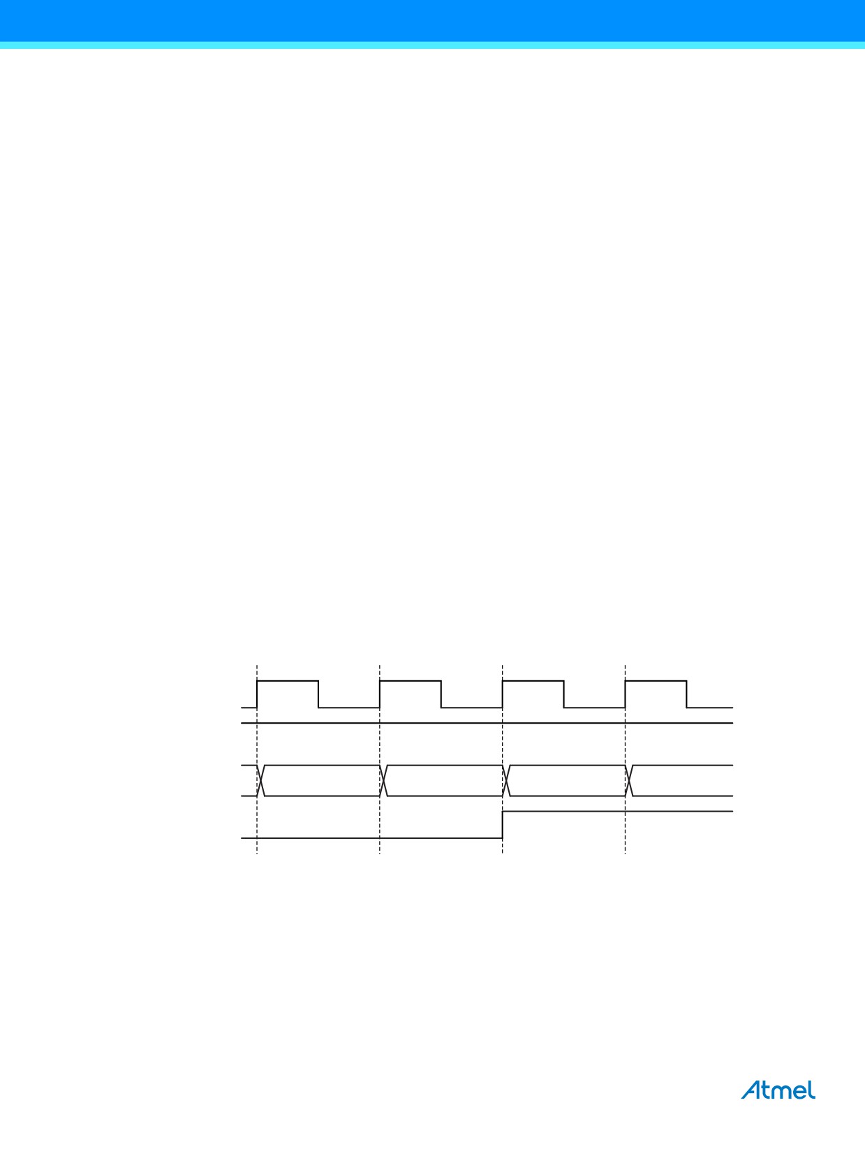
The Timer/Counter is a synchronous design and the timer clock (clkT0) is therefore shown as a clock enable signal in the
following figures. The figures include information on when interrupt flags are set. Figure 14-8 contains timing data for basic
Timer/Counter operation. The figure shows the count sequence close to the MAX value in all modes other than phase
correct PWM mode.
Figure 14-8. Timer/Counter Timing Diagram, no Prescaling
clkI/O
clkTn
(clkI/O/1)
TCNTn
MAX - 1
MAX
BOTTOM
BOTTOM + 1
TOVn
82
ATmega328P [DATASHEET]
7810D-AVR-01/15
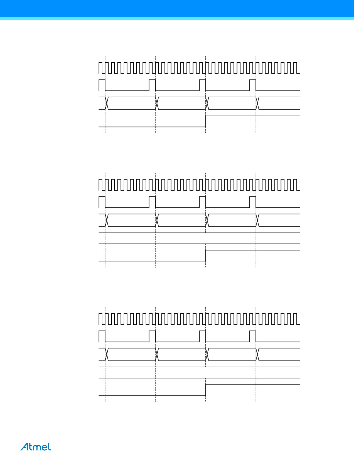
Figure 14-9 shows the same timing data, but with the prescaler enabled.
Figure 14-9. Timer/Counter Timing Diagram, with Prescaler (fclk_I/O/8)
clkI/O
clkTn
(clkI/O/8)
TCNTn
MAX - 1
MAX
BOTTOM
BOTTOM + 1
TOVn
Figure 14-10 shows the setting of OCF0B in all modes and OCF0A in all modes except CTC mode and PWM mode, where
OCR0A is TOP.
Figure 14-10. Timer/Counter Timing Diagram, Setting of OCF0x, with Prescaler (fclk_I/O/8)
clkI/O
clkTn
(clkI/O/8)
TCNTn
OCRnx - 1
OCRnx
OCRnx + 1
OCRnx + 2
OCRnx
OCRnx Value
OCFnx
Figure 14-11 shows the setting of OCF0A and the clearing of TCNT0 in CTC mode and fast PWM mode where OCR0A is
TOP.
Figure 14-11. Timer/Counter Timing Diagram, Clear Timer on Compare Match mode, with Prescaler (fclk_I/O/8)
clkI/O
clkTn
(clkI/O/8)
TCNTn
TOP - 1
TOP
BOTTOM
BOTTOM + 1
(CTC)
OCRnx
TOP
OCFnx
ATmega328P [DATASHEET]
83
7810D-AVR-01/15
14.9
Register Description
14.9.1
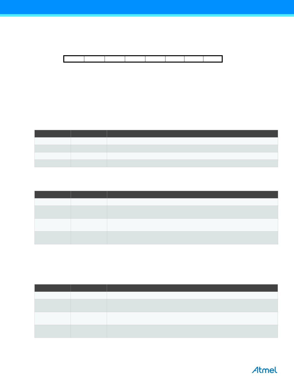
TCCR0A - Timer/Counter Control Register A
Bit
7
6
5
4
3
2
1
0
0x24 (0x44)
COM0A1
COM0A0
COM0B1
COM0B0
-
-
WGM01
WGM00
TCCR0A
Read/Write
R/W
R/W
R/W
R/W
R
R
R/W
R/W
Initial Value
0
0
0
0
0
0
0
0
• Bits 7:6 - COM0A1:0: Compare Match Output A Mode
These bits control the output compare pin (OC0A) behavior. If one or both of the COM0A1:0 bits are set, the OC0A output
overrides the normal port functionality of the I/O pin it is connected to. However, note that the data direction register (DDR)
bit corresponding to the OC0A pin must be set in order to enable the output driver.
When OC0A is connected to the pin, the function of the COM0A1:0 bits depends on the WGM02:0 bit setting. Table 14-2
shows the COM0A1:0 bit functionality when the WGM02:0 bits are set to a normal or CTC mode (non-PWM).
Table 14-2. Compare Output Mode, non-PWM Mode
COM0A1
COM0A0
Description
0
0
Normal port operation, OC0A disconnected.
0
1
Toggle OC0A on compare match
1
0
Clear OC0A on compare match
1
1
Set OC0A on compare match
Table 14-3 shows the COM0A1:0 bit functionality when the WGM01:0 bits are set to fast PWM mode.
Table 14-3. Compare Output Mode, Fast PWM Mode(1)
COM0A1
COM0A0
Description
0
0
Normal port operation, OC0A disconnected.
WGM02 = 0: Normal port operation, OC0A disconnected.
0
1
WGM02 = 1: Toggle OC0A on compare match.
Clear OC0A on compare match, set OC0A at BOTTOM,
1
0
(non-inverting mode).
Set OC0A on compare match, clear OC0A at BOTTOM,
1
1
(inverting mode).
Note:
1.
A special case occurs when OCR0A equals TOP and COM0A1 is set. In this case, the compare match is
ignored, but the set or clear is done at BOTTOM. See Section 14.7.3 “Fast PWM Mode” on page 80 for more
details.
Table 14-4 shows the COM0A1:0 bit functionality when the WGM02:0 bits are set to phase correct PWM mode.
Table 14-4. Compare Output Mode, Phase Correct PWM Mode(1)
COM0A1
COM0A0
Description
0
0
Normal port operation, OC0A disconnected.
WGM02 = 0: Normal port operation, OC0A disconnected.
0
1
WGM02 = 1: Toggle OC0A on compare match.
Clear OC0A on compare match when up-counting. Set OC0A on compare match
1
0
when down-counting.
Set OC0A on compare match when up-counting. Clear OC0A on compare match
1
1
when down-counting.
Note:
1.
A special case occurs when OCR0A equals TOP and COM0A1 is set. In this case, the compare match is
ignored, but the set or clear is done at TOP. See Section 15.9.4 “Phase Correct PWM Mode” on page 103 for
more details.
84
ATmega328P [DATASHEET]
7810D-AVR-01/15

• Bits 5:4 - COM0B1:0: Compare Match Output B Mode
These bits control the output compare pin (OC0B) behavior. If one or both of the COM0B1:0 bits are set, the OC0B output
overrides the normal port functionality of the I/O pin it is connected to. However, note that the data direction register (DDR)
bit corresponding to the OC0B pin must be set in order to enable the output driver.
When OC0B is connected to the pin, the function of the COM0B1:0 bits depends on the WGM02:0 bit setting. Table 14-5
shows the COM0B1:0 bit functionality when the WGM02:0 bits are set to a normal or CTC mode (non-PWM).
Table 14-5. Compare Output Mode, non-PWM Mode
COM0B1
COM0B0
Description
0
0
Normal port operation, OC0B disconnected.
0
1
Toggle OC0B on compare match
1
0
Clear OC0B on compare match
1
1
Set OC0B on compare match
Table 14-6 shows the COM0B1:0 bit functionality when the WGM02:0 bits are set to fast PWM mode.
Table 14-6. Compare Output Mode, Fast PWM Mode(1)
COM0B1
COM0B0
Description
0
0
Normal port operation, OC0B disconnected.
0
1
Reserved
Clear OC0B on compare match, set OC0B at BOTTOM,
1
0
(non-inverting mode)
Set OC0B on compare match, clear OC0B at BOTTOM,
1
1
(inverting mode).
Note:
1.
A special case occurs when OCR0B equals TOP and COM0B1 is set. In this case, the compare match is
ignored, but the set or clear is done at TOP. See Section 14.7.3 “Fast PWM Mode” on page 80 for more
details.
Table 14-7 shows the COM0B1:0 bit functionality when the WGM02:0 bits are set to phase correct PWM mode.
Table 14-7. Compare Output Mode, Phase Correct PWM Mode(1)
COM0B1
COM0B0
Description
0
0
Normal port operation, OC0B disconnected.
0
1
Reserved
Clear OC0B on compare match when up-counting. Set OC0B on compare match when
1
0
down-counting.
Set OC0B on compare match when up-counting. Clear OC0B on compare match when
1
1
down-counting.
Note:
1.
A special case occurs when OCR0B equals TOP and COM0B1 is set. In this case, the compare match is
ignored, but the set or clear is done at TOP. See Section 14.7.4 “Phase Correct PWM Mode” on page 81 for
more details.
• Bits 3, 2 - Res: Reserved Bits
These bits are reserved bits in the Atmel® ATmega328P and will always read as zero.
ATmega328P [DATASHEET]
85
7810D-AVR-01/15
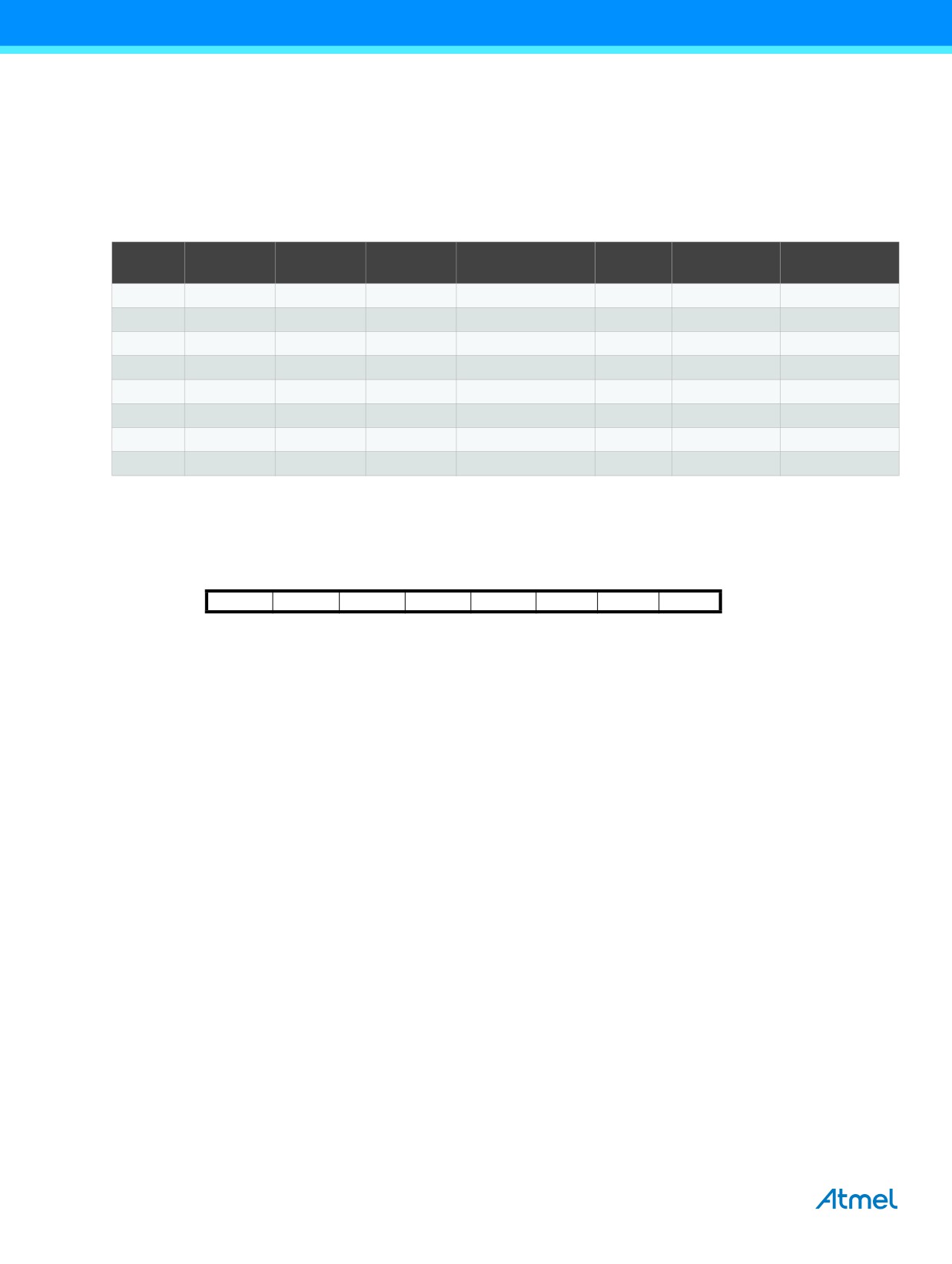
• Bits 1:0 - WGM01:0: Waveform Generation Mode
Combined with the WGM02 bit found in the TCCR0B register, these bits control the counting sequence of the counter, the
source for maximum (TOP) counter value, and what type of waveform generation to be used, see Table 14-8. Modes of
operation supported by the Timer/Counter unit are: Normal mode (counter), clear timer on compare match (CTC) mode, and
two types of pulse width modulation (PWM) modes (see Section 14.7 “Modes of Operation” on page 78).
Table 14-8. Waveform Generation Mode Bit Description
Timer/Counter
Update of
TOV Flag
Mode
WGM02
WGM01
WGM00
Mode of Operation
TOP
OCRx at
Set on(1)(2)
0
0
0
0
Normal
0xFF
Immediate
MAX
1
0
0
1
PWM, phase correct
0xFF
TOP
BOTTOM
2
0
1
0
CTC
OCRA
Immediate
MAX
3
0
1
1
Fast PWM
0xFF
BOTTOM
MAX
4
1
0
0
Reserved
-
-
-
5
1
0
1
PWM, phase correct
OCRA
TOP
BOTTOM
6
1
1
0
Reserved
-
-
-
7
1
1
1
Fast PWM
OCRA
BOTTOM
TOP
Notes:
1.
MAX
= 0xFF
2.
BOTTOM = 0x00
14.9.2
TCCR0B - Timer/Counter Control Register B
Bit
7
6
5
4
3
2
1
0
0x25 (0x45)
FOC0A
FOC0B
-
-
WGM02
CS02
CS01
CS00
TCCR0B
Read/Write
W
W
R
R
R/W
R/W
R/W
R/W
Initial Value
0
0
0
0
0
0
0
0
• Bit 7 - FOC0A: Force Output Compare A
The FOC0A bit is only active when the WGM bits specify a non-PWM mode.
However, for ensuring compatibility with future devices, this bit must be set to zero when TCCR0B is written when operating
in PWM mode. When writing a logical one to the FOC0A bit, an immediate compare match is forced on the waveform
generation unit. The OC0A output is changed according to its COM0A1:0 bits setting. Note that the FOC0A bit is
implemented as a strobe. Therefore it is the value present in the COM0A1:0 bits that determines the effect of the forced
compare.
A FOC0A strobe will not generate any interrupt, nor will it clear the timer in CTC mode using OCR0A as TOP.
The FOC0A bit is always read as zero.
• Bit 6 - FOC0B: Force Output Compare B
The FOC0B bit is only active when the WGM bits specify a non-PWM mode.
However, for ensuring compatibility with future devices, this bit must be set to zero when TCCR0B is written when operating
in PWM mode. When writing a logical one to the FOC0B bit, an immediate compare match is forced on the waveform
generation unit. The OC0B output is changed according to its COM0B1:0 bits setting. Note that the FOC0B bit is
implemented as a strobe. Therefore it is the value present in the COM0B1:0 bits that determines the effect of the forced
compare.
A FOC0B strobe will not generate any interrupt, nor will it clear the timer in CTC mode using OCR0B as TOP.
The FOC0B bit is always read as zero.
• Bits 5:4 - Res: Reserved Bits
These bits are reserved bits in the ATmega328P and will always read as zero.
86
ATmega328P [DATASHEET]
7810D-AVR-01/15
• Bit 3 - WGM02: Waveform Generation Mode
See the description in the Section 14.9.1 “TCCR0A - Timer/Counter Control Register A” on page 84.
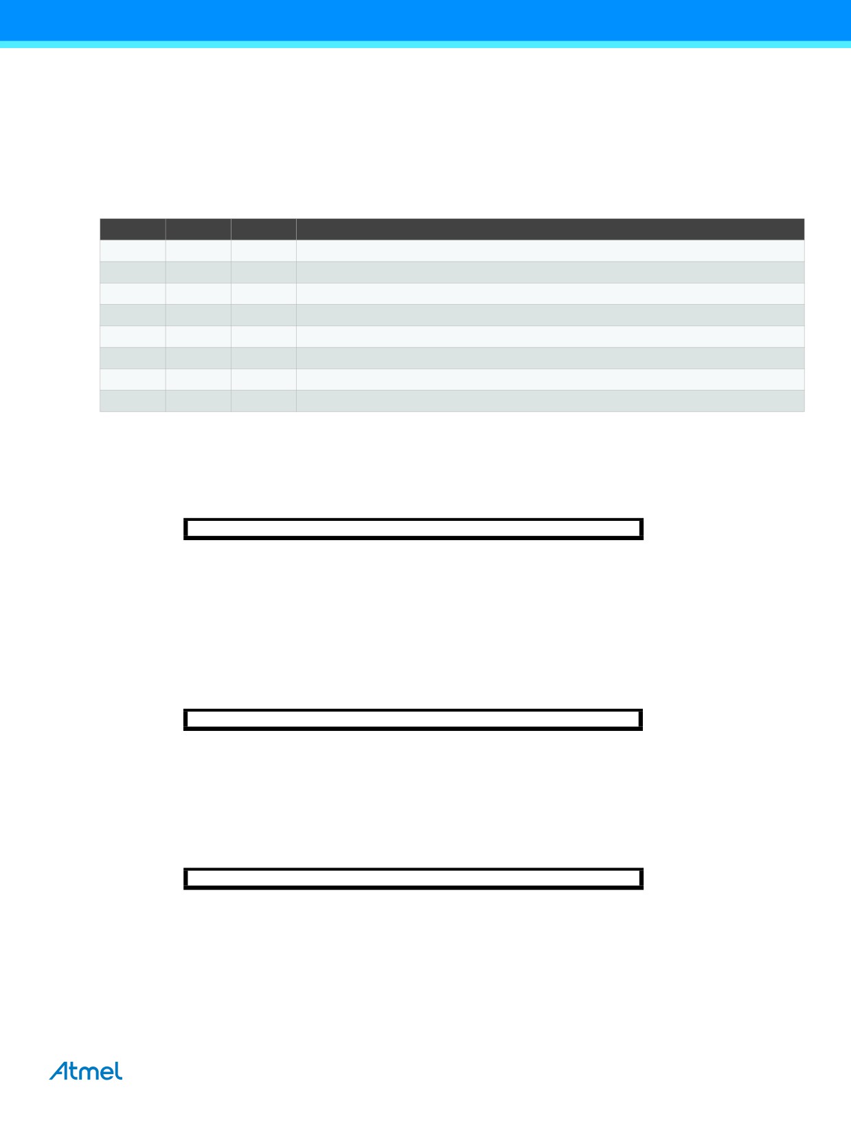
• Bits 2:0 - CS02:0: Clock Select
The three clock select bits select the clock source to be used by the Timer/Counter.
Table 14-9. Clock Select Bit Description
CS02
CS01
CS00
Description
0
0
0
No clock source (Timer/Counter stopped)
0
0
1
clkI/O/(no prescaling)
0
1
0
clkI/O/8 (from prescaler)
0
1
1
clkI/O/64 (from prescaler)
1
0
0
clkI/O/256 (from prescaler)
1
0
1
clkI/O/1024 (from prescaler)
1
1
0
External clock source on T0 pin. Clock on falling edge.
1
1
1
External clock source on T0 pin. Clock on rising edge.
If external pin modes are used for the Timer/Counter0, transitions on the T0 pin will clock the counter even if the pin is
configured as an output. This feature allows software control of the counting.
14.9.3
TCNT0 - Timer/Counter Register
Bit
7
6
5
4
3
2
1
0
0x26 (0x46)
TCNT0[7:0]
TCNT0
Read/Write
R/W
R/W
R/W
R/W
R/W
R/W
R/W
R/W
Initial Value
0
0
0
0
0
0
0
0
The Timer/Counter register gives direct access, both for read and write operations, to the Timer/Counter unit 8-bit counter.
Writing to the TCNT0 register blocks (removes) the compare match on the following timer clock. Modifying the counter
(TCNT0) while the counter is running, introduces a risk of missing a compare match between TCNT0 and the OCR0x
registers.
14.9.4
OCR0A - Output Compare Register A
Bit
7
6
5
4
3
2
1
0
0x27 (0x47)
OCR0A[7:0]
OCR0A
Read/Write
R/W
R/W
R/W
R/W
R/W
R/W
R/W
R/W
Initial Value
0
0
0
0
0
0
0
0
The output compare register A contains an 8-bit value that is continuously compared with the counter value (TCNT0). A
match can be used to generate an output compare interrupt, or to generate a waveform output on the OC0A pin.
14.9.5
OCR0B - Output Compare Register B
Bit
7
6
5
4
3
2
1
0
0x28 (0x48)
OCR0B[7:0]
OCR0B
Read/Write
R/W
R/W
R/W
R/W
R/W
R/W
R/W
R/W
Initial Value
0
0
0
0
0
0
0
0
The output compare register B contains an 8-bit value that is continuously compared with the counter value (TCNT0). A
match can be used to generate an output compare interrupt, or to generate a waveform output on the OC0B pin.
ATmega328P [DATASHEET]
87
7810D-AVR-01/15
14.9.6
TIMSK0 - Timer/Counter Interrupt Mask Register
Bit
7
6
5
4
3
2
1
0
(0x6E)
-
-
-
-
-
OCIE0B
OCIE0A
TOIE0
TIMSK0
Read/Write
R
R
R
R
R
R/W
R/W
R/W
Initial Value
0
0
0
0
0
0
0
0
• Bits 7..3 - Res: Reserved Bits
These bits are reserved bits in the Atmel® ATmega328P and will always read as zero.
• Bit 2 - OCIE0B: Timer/Counter Output Compare Match B Interrupt Enable
When the OCIE0B bit is written to one, and the I-bit in the status register is set, the Timer/Counter compare match B interrupt
is enabled. The corresponding interrupt is executed if a compare match in Timer/Counter occurs, i.e., when the OCF0B bit is
set in the Timer/Counter interrupt flag register - TIFR0.
• Bit 1 - OCIE0A: Timer/Counter0 Output Compare Match A Interrupt Enable
When the OCIE0A bit is written to one, and the I-bit in the status register is set, the Timer/Counter0 compare match A
interrupt is enabled. The corresponding interrupt is executed if a compare match in Timer/Counter0 occurs, i.e., when the
OCF0A bit is set in the Timer/Counter 0 interrupt flag register - TIFR0.
• Bit 0 - TOIE0: Timer/Counter0 Overflow Interrupt Enable
When the TOIE0 bit is written to one, and the I-bit in the status register is set, the Timer/Counter0 overflow interrupt is
enabled. The corresponding interrupt is executed if an overflow in Timer/Counter0 occurs, i.e., when the TOV0 bit is set in
the Timer/Counter 0 interrupt flag register - TIFR0.
14.9.7
TIFR0 - Timer/Counter 0 Interrupt Flag Register
Bit
7
6
5
4
3
2
1
0
0x15 (0x35)
-
-
-
-
-
OCF0B
OCF0A
TOV0
TIFR0
Read/Write
R
R
R
R
R
R/W
R/W
R/W
Initial Value
0
0
0
0
0
0
0
0
• Bits 7..3 - Res: Reserved Bits
These bits are reserved bits in the Atmel ATmega328P and will always read as zero.
• Bit 2 - OCF0B: Timer/Counter 0 Output Compare B Match Flag
The OCF0B bit is set when a compare match occurs between the Timer/Counter and the data in OCR0B - output compare
register0 B. OCF0B is cleared by hardware when executing the corresponding interrupt handling vector. Alternatively,
OCF0B is cleared by writing a logic one to the flag. When the I-bit in SREG, OCIE0B (Timer/Counter compare B match
interrupt enable), and OCF0B are set, the Timer/Counter compare match interrupt is executed.
• Bit 1 - OCF0A: Timer/Counter 0 Output Compare A Match Flag
The OCF0A bit is set when a compare match occurs between the Timer/Counter0 and the data in OCR0A - output compare
register0. OCF0A is cleared by hardware when executing the corresponding interrupt handling vector. Alternatively, OCF0A
is cleared by writing a logic one to the flag. When the I-bit in SREG, OCIE0A (Timer/Counter0 compare match interrupt
enable), and OCF0A are set, the Timer/Counter0 compare match interrupt is executed.
• Bit 0 - TOV0: Timer/Counter0 Overflow Flag
The bit TOV0 is set when an overflow occurs in Timer/Counter0. TOV0 is cleared by hardware when executing the
corresponding interrupt handling vector. Alternatively, TOV0 is cleared by writing a logic one to the flag. When the
SREG I-bit, TOIE0 (Timer/Counter0 overflow interrupt enable), and TOV0 are set, the Timer/Counter0 overflow interrupt is
executed.
The setting of this flag is dependent of the WGM02:0 bit setting. Refer to Table 14-8 on page 86, Section 14-8 “Waveform
Generation Mode Bit Description” on page 86.
88
ATmega328P [DATASHEET]
7810D-AVR-01/15
15.
16-bit Timer/Counter1 with PWM
15.1
Features
● True 16-bit design (i.e., allows 16-bit PWM)
● Two independent output compare units
● Double buffered output compare registers
● One input capture unit
● Input capture noise canceler
● Clear timer on compare match (auto reload)
● Glitch-free, phase correct pulse width modulator (PWM)
● Variable PWM period
● Frequency generator
● External event counter
● Four independent interrupt sources (TOV1, OCF1A, OCF1B, and ICF1)
15.2
Overview
The 16-bit Timer/Counter unit allows accurate program execution timing (event management), wave generation, and signal
timing measurement.
Most register and bit references in this section are written in general form. A lower case “n” replaces the Timer/Counter
number, and a lower case “x” replaces the output compare unit channel. However, when using the register or bit defines in a
program, the precise form must be used, i.e., TCNT1 for accessing Timer/Counter1 counter value and so on.
A simplified block diagram of the 16-bit Timer/Counter is shown in Figure 15-1 on page 90. For the actual placement of I/O
pins, refer to Section 1-1 “Pinout” on page 3. CPU accessible I/O registers, including I/O bits and I/O pins, are shown in bold.
The device-specific I/O register and bit locations are listed in the Section 15.11 “Register Description” on page 108.
The PRTIM1 bit in Section 9.11.3 “PRR - Power Reduction Register” on page 38 must be written to zero to enable
Timer/Counter1 module.
ATmega328P [DATASHEET]
89
7810D-AVR-01/15
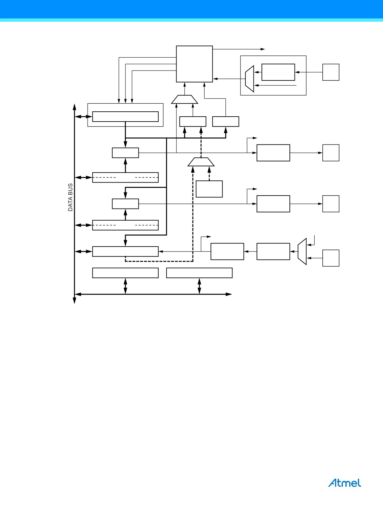
Figure 15-1.
16-bit Timer/Counter Block Diagram(1)
TOVn (Int. Req.)
Count
Clear
Clock Select
Control Logic
Direction
Edge
Tn
clkTn
Detector
(from Prescaler)
TOP
BOTTOM
Timer/Counter
TCNTn
=
= 0
OCnA (Int. Req.)
Waveform
OCnA
=
Generation
OCRnA
Fixed
TOP
OCnB (Int. Req.)
Values
Waveform
OCnB
=
Generation
OCRnB
(From Analog
Comparator Output)
ICFn (Int. Req.)
Edge
Noise
ICRn
Detector
Canceler
ICPn
TCCRnA
TCCRnB
Note:
1.
Refer to Figure 1-1 on page 3, Table 13-3 on page 65 and Table 13-9 on page 70 for Timer/Counter1 pin
placement and description.
15.2.1
Registers
The Timer/Counter (TCNT1), output compare registers (OCR1A/B), and input capture register (ICR1) are all 16-bit registers.
Special procedures must be followed when accessing the 16-bit registers. These procedures are described in the Section
15.3 “Accessing 16-bit Registers” on page 91. The Timer/Counter control registers (TCCR1A/B) are 8-bit registers and have
no CPU access restrictions. Interrupt requests (abbreviated to Int.Req. in the figure) signals are all visible in the timer
interrupt flag register (TIFR1). All interrupts are individually masked with the timer interrupt mask register (TIMSK1). TIFR1
and TIMSK1 are not shown in the figure.
The Timer/Counter can be clocked internally, via the prescaler, or by an external clock source on the T1 pin. The clock select
logic block controls which clock source and edge the Timer/Counter uses to increment (or decrement) its value. The
Timer/Counter is inactive when no clock source is selected. The output from the clock select logic is referred to as the timer
clock (clkT1).
90
ATmega328P [DATASHEET]
7810D-AVR-01/15
The double buffered output compare registers (OCR1A/B) are compared with the Timer/Counter value at all time. The result
of the compare can be used by the waveform generator to generate a PWM or variable frequency output on the output
compare pin (OC1A/B). See Section 15.7 “Output Compare Units” on page 97. The compare match event will also set the
compare match flag (OCF1A/B) which can be used to generate an output compare interrupt request.
The input capture register can capture the Timer/Counter value at a given external (edge triggered) event on either the input
capture pin (ICP1) or on the analog comparator pins (see Section 22. “Analog Comparator” on page 202). The input capture
unit includes a digital filtering unit (noise canceler) for reducing the chance of capturing noise spikes.
The TOP value, or maximum Timer/Counter value, can in some modes of operation be defined by either the OCR1A
register, the ICR1 register, or by a set of fixed values. When using OCR1A as TOP value in a PWM mode, the OCR1A
register can not be used for generating a PWM output. However, the TOP value will in this case be double buffered allowing
the TOP value to be changed in run time. If a fixed TOP value is required, the ICR1 register can be used as an alternative,
freeing the OCR1A to be used as PWM output.
15.2.2
Definitions
The following definitions are used extensively throughout the section:
Table 15-1. Definitions
Parameter
Definition
BOTTOM
The counter reaches the BOTTOM when it becomes 0x0000.
MAX
The counter reaches its MAXimum when it becomes 0xFFFF (decimal 65535).
The counter reaches the TOP when it becomes equal to the highest value in the count sequence. The TOP
TOP
value can be assigned to be one of the fixed values: 0x00FF, 0x01FF, or 0x03FF, or to the value stored in
the OCR1A or ICR1 register. The assignment is dependent of the mode of operation.
15.3
Accessing 16-bit Registers
The TCNT1, OCR1A/B, and ICR1 are 16-bit registers that can be accessed by the AVR® CPU via the 8-bit data bus.
The 16-bit register must be byte accessed using two read or write operations. Each 16-bit timer has a single 8-bit register for
temporary storing of the high byte of the 16-bit access. The same temporary register is shared between all 16-bit registers
within each 16-bit timer. Accessing the low byte triggers the 16-bit read or write operation. When the low byte of a 16-bit
register is written by the CPU, the high byte stored in the temporary register, and the low byte written are both copied into the
16-bit register in the same clock cycle. When the low byte of a 16-bit register is read by the CPU, the high byte of the 16-bit
register is copied into the temporary register in the same clock cycle as the low byte is read.
Not all 16-bit accesses uses the temporary register for the high byte. Reading the OCR1A/B 16-bit registers does not involve
using the temporary register.
To do a 16-bit write, the high byte must be written before the low byte. For a 16-bit read, the low byte must be read before the
high byte.
ATmega328P [DATASHEET]
91
7810D-AVR-01/15
The following code examples show how to access the 16-bit timer registers assuming that no interrupts updates the
temporary register. The same principle can be used directly for accessing the OCR1A/B and ICR1 registers. Note that when
using “C”, the compiler handles the 16-bit access.
Assembly Code Examples(1)
; Set TCNT1 to 0x01FF
ldi
r17,0x01
ldi
r16,0xFF
out
TCNT1H,r17
out
TCNT1L,r16
; Read TCNT1 into r17:r16
in
r16,TCNT1L
in
r17,TCNT1H
C Code Examples(1)
unsigned int i;
/* Set TCNT1 to 0x01FF */
TCNT1 = 0x1FF;
/* Read TCNT1 into i */
i = TCNT1;
Note:
1.
See Section 5. “About Code Examples” on page 8
For I/O registers located in extended I/O map, “IN”, “OUT”, “SBIS”, “SBIC”, “CBI”, and “SBI” instructions must
be replaced with instructions that allow access to extended I/O. Typically “LDS” and “STS” combined with
“SBRS”, “SBRC”, “SBR”, and “CBR”.
The assembly code example returns the TCNT1 value in the r17:r16 register pair.
It is important to notice that accessing 16-bit registers are atomic operations. If an interrupt occurs between the two
instructions accessing the 16-bit register, and the interrupt code updates the temporary register by accessing the same or
any other of the 16-bit timer registers, then the result of the access outside the interrupt will be corrupted. Therefore, when
both the main code and the interrupt code update the temporary register, the main code must disable the interrupts during
the 16-bit access.
92
ATmega328P [DATASHEET]
7810D-AVR-01/15
The following code examples show how to do an atomic read of the TCNT1 register contents. Reading any of the OCR1A/B
or ICR1 registers can be done by using the same principle.
Assembly Code Example(1)
TIM16_ReadTCNT1:
; Save global interrupt flag
in
r18,SREG
; Disable interrupts
cli
; Read TCNT1 into r17:r16
in
r16,TCNT1L
in
r17,TCNT1H
; Restore global interrupt flag
out
SREG,r18
ret
C Code Example(1)
unsigned int TIM16_ReadTCNT1( void )
{
unsigned char sreg;
unsigned int i;
/* Save global interrupt flag */
sreg = SREG;
/* Disable interrupts */
_CLI();
/* Read TCNT1 into i */
i = TCNT1;
/* Restore global interrupt flag */
SREG = sreg;
return i;
}
Note:
1.
See Section 5. “About Code Examples” on page 8.
For I/O registers located in extended I/O map, “IN”, “OUT”, “SBIS”, “SBIC”, “CBI”, and “SBI” instructions must
be replaced with instructions that allow access to extended I/O. Typically “LDS” and “STS” combined with
“SBRS”, “SBRC”, “SBR”, and “CBR”.
The assembly code example returns the TCNT1 value in the r17:r16 register pair.
ATmega328P [DATASHEET]
93
7810D-AVR-01/15
The following code examples show how to do an atomic write of the TCNT1 register contents. Writing any of the OCR1A/B
or ICR1 registers can be done by using the same principle.
Assembly Code Example(1)
TIM16_WriteTCNT1:
; Save global interrupt flag
in
r18,SREG
; Disable interrupts
cli
; Set TCNT1 to r17:r16
out
TCNT1H,r17
out
TCNT1L,r16
; Restore global interrupt flag
out
SREG,r18
ret
C Code Example(1)
void TIM16_WriteTCNT1(unsigned int i)
{
unsigned char sreg;
unsigned int i;
/* Save global interrupt flag */
sreg = SREG;
/* Disable interrupts */
_CLI();
/* Set TCNT1 to i */
TCNT1 = i;
/* Restore global interrupt flag */
SREG = sreg;
}
Note:
1.
See Section 5. “About Code Examples” on page 8.
For I/O registers located in extended I/O map, “IN”, “OUT”, “SBIS”, “SBIC”, “CBI”, and “SBI” instructions must
be replaced with instructions that allow access to extended I/O. Typically “LDS” and “STS” combined with
“SBRS”, “SBRC”, “SBR”, and “CBR”.
The assembly code example requires that the r17:r16 register pair contains the value to be written to TCNT1.
15.3.1
Reusing the Temporary High Byte Register
If writing to more than one 16-bit register where the high byte is the same for all registers written, then the high byte only
needs to be written once. However, note that the same rule of atomic operation described previously also applies in this
case.
15.4
Timer/Counter Clock Sources
The Timer/Counter can be clocked by an internal or an external clock source. The clock source is selected by the clock
select logic which is controlled by the clock select (CS12:0) bits located in the Timer/Counter control register B (TCCR1B).
For details on clock sources and prescaler, see Section 16. “Timer/Counter0 and Timer/Counter1 Prescalers” on page 114.
94
ATmega328P [DATASHEET]
7810D-AVR-01/15
15.5
Counter Unit
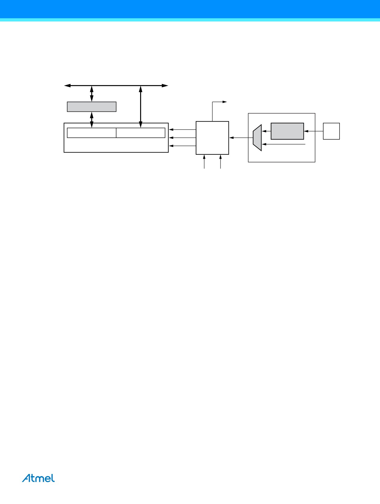
The main part of the 16-bit Timer/Counter is the programmable 16-bit bi-directional counter unit. Figure 15-2 shows a block
diagram of the counter and its surroundings.
Figure 15-2. Counter Unit Block Diagram
DATA BUS (8-bit)
TOVn
(Int. Req.)
TEMP (8-bit)
Clock Select
Count
Edge
TCNTnH (8-bit)
TCNTnL (8-bit)
Tn
Clear
clk
Tn
Detector
Control Logic
Direction
TCNTnH (16-bit Counter)
(from Prescaler)
TOP
BOTTOM
Signal description (internal signals):
Count
Increment or decrement TCNT1 by 1.
Direction
Select between increment and decrement.
Clear
Clear TCNT1 (set all bits to zero).
clkT1
Timer/Counter clock.
TOP
Signalize that TCNT1 has reached maximum value.
BOTTOM
Signalize that TCNT1 has reached minimum value (zero).
The 16-bit counter is mapped into two 8-bit I/O memory locations: Counter high (TCNT1H) containing the upper eight bits of
the counter, and counter low (TCNT1L) containing the lower eight bits. The TCNT1H register can only be indirectly accessed
by the CPU. When the CPU does an access to the TCNT1H I/O location, the CPU accesses the high byte temporary register
(TEMP). The temporary register is updated with the TCNT1H value when the TCNT1L is read, and TCNT1H is updated with
the temporary register value when TCNT1L is written. This allows the CPU to read or write the entire 16-bit counter value
within one clock cycle via the 8-bit data bus. It is important to notice that there are special cases of writing to the TCNT1
register when the counter is counting that will give unpredictable results. The special cases are described in the sections
where they are of importance.
Depending on the mode of operation used, the counter is cleared, incremented, or decremented at each timer clock (clkT1).
The clkT1 can be generated from an external or internal clock source, selected by the clock select bits (CS12:0). When no
clock source is selected (CS12:0 = 0) the timer is stopped. However, the TCNT1 value can be accessed by the CPU,
independent of whether clkT1 is present or not. A CPU write overrides (has priority over) all counter clear or count
operations.
The counting sequence is determined by the setting of the waveform generation mode bits (WGM13:0) located in the
Timer/Counter control registers A and B (TCCR1A and TCCR1B). There are close connections between how the counter
behaves (counts) and how waveforms are generated on the output compare outputs OC1x. For more details about
advanced counting sequences and waveform generation, see Section 15.9 “Modes of Operation” on page 100.
The Timer/Counter overflow flag (TOV1) is set according to the mode of operation selected by the WGM13:0 bits. TOV1 can
be used for generating a CPU interrupt.
15.6
Input Capture Unit
The Timer/Counter incorporates an input capture unit that can capture external events and give them a time-stamp
indicating time of occurrence. The external signal indicating an event, or multiple events, can be applied via the ICP1 pin or
alternatively, via the analog-comparator unit. The time-stamps can then be used to calculate frequency, duty-cycle, and
other features of the signal applied. Alternatively the time-stamps can be used for creating a log of the events.
The input capture unit is illustrated by the block diagram shown in Figure 15-3 on page 96. The elements of the block
diagram that are not directly a part of the input capture unit are gray shaded. The small “n” in register and bit names
indicates the Timer/Counter number.
ATmega328P [DATASHEET]
95
7810D-AVR-01/15
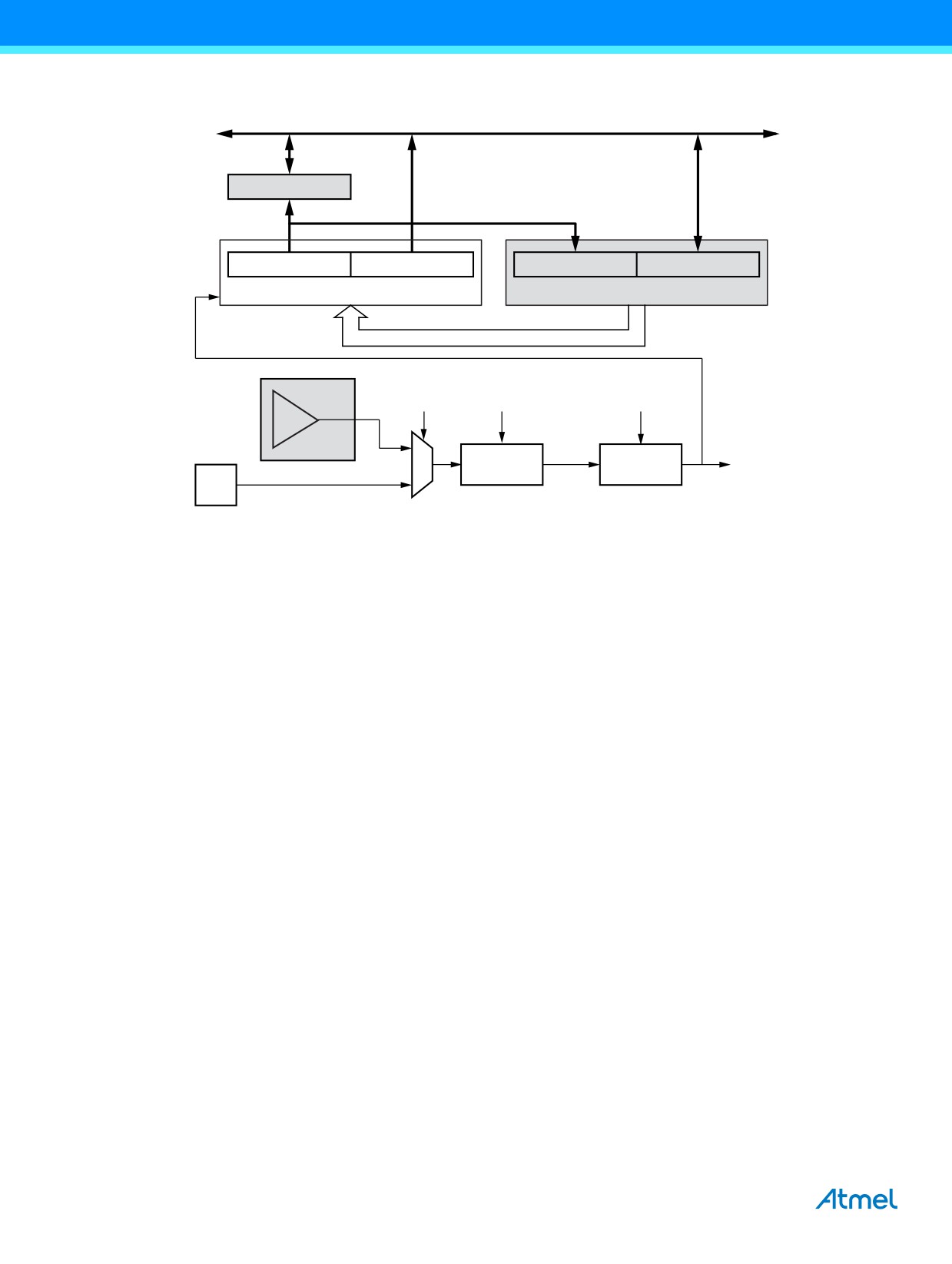
Figure 15-3. Input Capture Unit Block Diagram
DATA BUS (8-bit)
TEMP (8-bit)
ICRnH (8-bit)
ICRnL (8-bit)
TCNTnH (8-bit)
TCNTnL (8-bit)
ICRn (16-bit Register)
TCNTn (16-bit Counter)
WRITE
+
ACO*
ACIC*
ICNC
ICES
-
Analog
Comparator
Noise
Edge
ICFn (Int. Req.)
Canceler
Detector
ICPn
When a change of the logic level (an event) occurs on the input capture pin (ICP1), alternatively on the analog comparator
output (ACO), and this change confirms to the setting of the edge detector, a capture will be triggered. When a capture is
triggered, the 16-bit value of the counter (TCNT1) is written to the input capture register (ICR1). The input capture flag (ICF1)
is set at the same system clock as the TCNT1 value is copied into ICR1 register. If enabled (ICIE1 = 1), the input capture flag
generates an input capture interrupt. The ICF1 flag is automatically cleared when the interrupt is executed. Alternatively the
ICF1 flag can be cleared by software by writing a logical one to its I/O bit location.
Reading the 16-bit value in the input capture register (ICR1) is done by first reading the low byte (ICR1L) and then the high
byte (ICR1H). When the low byte is read the high byte is copied into the high byte temporary register (TEMP). When the
CPU reads the ICR1H I/O location it will access the TEMP register.
The ICR1 register can only be written when using a waveform generation mode that utilizes the ICR1 register for defining the
counter’s TOP value. In these cases the waveform generation mode (WGM13:0) bits must be set before the TOP value can
be written to the ICR1 register. When writing the ICR1 register the high byte must be written to the ICR1H I/O location before
the low byte is written to ICR1L.
For more information on how to access the 16-bit registers refer to Section 15.3 “Accessing 16-bit Registers” on page 91.
15.6.1
Input Capture Trigger Source
The main trigger source for the input capture unit is the input capture pin (ICP1). Timer/Counter1 can alternatively use the
analog comparator output as trigger source for the input capture unit. The analog comparator is selected as trigger source by
setting the analog comparator input capture (ACIC) bit in the analog comparator control and status register (ACSR). Be
aware that changing trigger source can trigger a capture. The input capture flag must therefore be cleared after the change.
Both the input capture pin (ICP1) and the analog comparator output (ACO) inputs are sampled using the same technique as
for the T1 pin (Figure 16-1 on page 114). The edge detector is also identical. However, when the noise canceler is enabled,
additional logic is inserted before the edge detector, which increases the delay by four system clock cycles. Note that the
input of the noise canceler and edge detector is always enabled unless the Timer/Counter is set in a waveform generation
mode that uses ICR1 to define TOP.
An input capture can be triggered by software by controlling the port of the ICP1 pin.
96
ATmega328P [DATASHEET]
7810D-AVR-01/15
15.6.2
Noise Canceler
The noise canceler improves noise immunity by using a simple digital filtering scheme. The noise canceler input is monitored
over four samples, and all four must be equal for changing the output that in turn is used by the edge detector.
The noise canceler is enabled by setting the input capture noise canceler (ICNC1) bit in Timer/Counter control register B
(TCCR1B). When enabled the noise canceler introduces additional four system clock cycles of delay from a change applied
to the input, to the update of the ICR1 register. The noise canceler uses the system clock and is therefore not affected by the
prescaler.
15.6.3
Using the Input Capture Unit
The main challenge when using the input capture unit is to assign enough processor capacity for handling the incoming
events. The time between two events is critical. If the processor has not read the captured value in the ICR1 register before
the next event occurs, the ICR1 will be overwritten with a new value. In this case the result of the capture will be incorrect.
When using the input capture interrupt, the ICR1 register should be read as early in the interrupt handler routine as possible.
Even though the input capture interrupt has relatively high priority, the maximum interrupt response time is dependent on the
maximum number of clock cycles it takes to handle any of the other interrupt requests.
Using the input capture unit in any mode of operation when the TOP value (resolution) is actively changed during operation,
is not recommended.
Measurement of an external signal’s duty cycle requires that the trigger edge is changed after each capture. Changing the
edge sensing must be done as early as possible after the ICR1 register has been read. After a change of the edge, the input
capture flag (ICF1) must be cleared by software (writing a logical one to the I/O bit location). For measuring frequency only,
the clearing of the ICF1 flag is not required (if an interrupt handler is used).
15.7
Output Compare Units
The 16-bit comparator continuously compares TCNT1 with the output compare register (OCR1x). If TCNT equals OCR1x
the comparator signals a match. A match will set the output compare flag (OCF1x) at the next timer clock cycle. If enabled
(OCIE1x = 1), the output compare flag generates an output compare interrupt. The OCF1x flag is automatically cleared
when the interrupt is executed. Alternatively the OCF1x flag can be cleared by software by writing a logical one to its I/O bit
location. The waveform generator uses the match signal to generate an output according to operating mode set by the
waveform generation mode (WGM13:0) bits and compare output mode (COM1x1:0) bits. The TOP and BOTTOM signals
are used by the waveform generator for handling the special cases of the extreme values in some modes of operation (see
Section 15.9 “Modes of Operation” on page 100).
A special feature of output compare unit A allows it to define the Timer/Counter TOP value (i.e., counter resolution). In
addition to the counter resolution, the TOP value defines the period time for waveforms generated by the waveform
generator.
Figure 15-4 on page 98 shows a block diagram of the output compare unit. The small “n” in the register and bit names
indicates the device number (n = 1 for Timer/Counter 1), and the “x” indicates output compare unit (A/B). The elements of the
block diagram that are not directly a part of the output compare unit are gray shaded.
ATmega328P [DATASHEET]
97
7810D-AVR-01/15
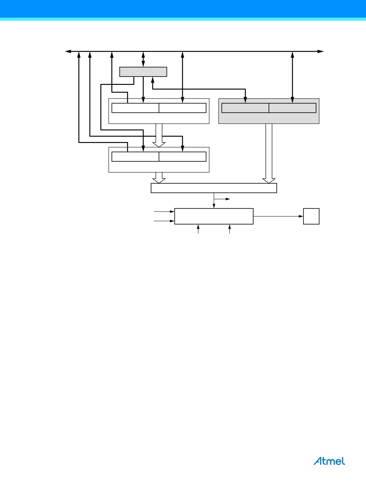
Figure 15-4. Output Compare Unit, Block Diagram
DATA BUS (8-bit)
TEMP (8-bit)
OCRnxH Buf. (8-bit)
OCRnxL Buf. (8-bit)
TCNTnH (8-bit)
TCNTnL (8-bit)
OCRnx Buffer (16-bit Register)
TCNTn (16-bit Counter)
OCRnxH (8-bit)
OCRnxL (8-bit)
OCRnx (16-bit Register)
= (16-bitComparator)
OCFnx (Int. Req.)
TOP
Waveform Generator
OCnx
BOTTOM
WGMn3:0
COMnx1:0
The OCR1x register is double buffered when using any of the twelve pulse width modulation (PWM) modes. For the normal
and clear timer on compare (CTC) modes of operation, the double buffering is disabled. The double buffering synchronizes
the update of the OCR1x compare register to either TOP or BOTTOM of the counting sequence. The synchronization
prevents the occurrence of odd-length, non-symmetrical PWM pulses, thereby making the output glitch-free.
The OCR1x register access may seem complex, but this is not case. When the double buffering is enabled, the CPU has
access to the OCR1x buffer register, and if double buffering is disabled the CPU will access the OCR1x directly. The content
of the OCR1x (buffer or compare) register is only changed by a write operation (the Timer/Counter does not update this
register automatically as the TCNT1 and ICR1 register). Therefore OCR1x is not read via the high byte temporary register
(TEMP). However, it is a good practice to read the low byte first as when accessing other 16-bit registers. Writing the OCR1x
registers must be done via the TEMP register since the compare of all 16 bits is done continuously. The high byte (OCR1xH)
has to be written first. When the high byte I/O location is written by the CPU, the TEMP register will be updated by the value
written. Then when the low byte (OCR1xL) is written to the lower eight bits, the high byte will be copied into the upper 8-bits
of either the OCR1x buffer or OCR1x compare register in the same system clock cycle.
For more information of how to access the 16-bit registers refer to Section 15.3 “Accessing 16-bit Registers” on page 91.
15.7.1
Force Output Compare
In non-PWM waveform generation modes, the match output of the comparator can be forced by writing a one to the force
output compare (FOC1x) bit. Forcing compare match will not set the OCF1x flag or reload/clear the timer, but the OC1x pin
will be updated as if a real compare match had occurred (the COM11:0 bits settings define whether the OC1x pin is set,
cleared or toggled).
15.7.2
Compare Match Blocking by TCNT1 Write
All CPU writes to the TCNT1 register will block any compare match that occurs in the next timer clock cycle, even when the
timer is stopped. This feature allows OCR1x to be initialized to the same value as TCNT1 without triggering an interrupt
when the Timer/Counter clock is enabled.
98
ATmega328P [DATASHEET]
7810D-AVR-01/15
15.7.3
Using the Output Compare Unit
Since writing TCNT1 in any mode of operation will block all compare matches for one timer clock cycle, there are risks
involved when changing TCNT1 when using any of the output compare channels, independent of whether the Timer/Counter
is running or not. If the value written to TCNT1 equals the OCR1x value, the compare match will be missed, resulting in
incorrect waveform generation. Do not write the TCNT1 equal to TOP in PWM modes with variable TOP values. The
compare match for the TOP will be ignored and the counter will continue to 0xFFFF. Similarly, do not write the TCNT1 value
equal to BOTTOM when the counter is downcounting.
The setup of the OC1x should be performed before setting the data direction register for the port pin to output. The easiest
way of setting the OC1x value is to use the force output compare (FOC1x) strobe bits in normal mode. The OC1x register
keeps its value even when changing between waveform generation modes.
Be aware that the COM1x1:0 bits are not double buffered together with the compare value. Changing the COM1x1:0 bits will
take effect immediately.
15.8
Compare Match Output Unit
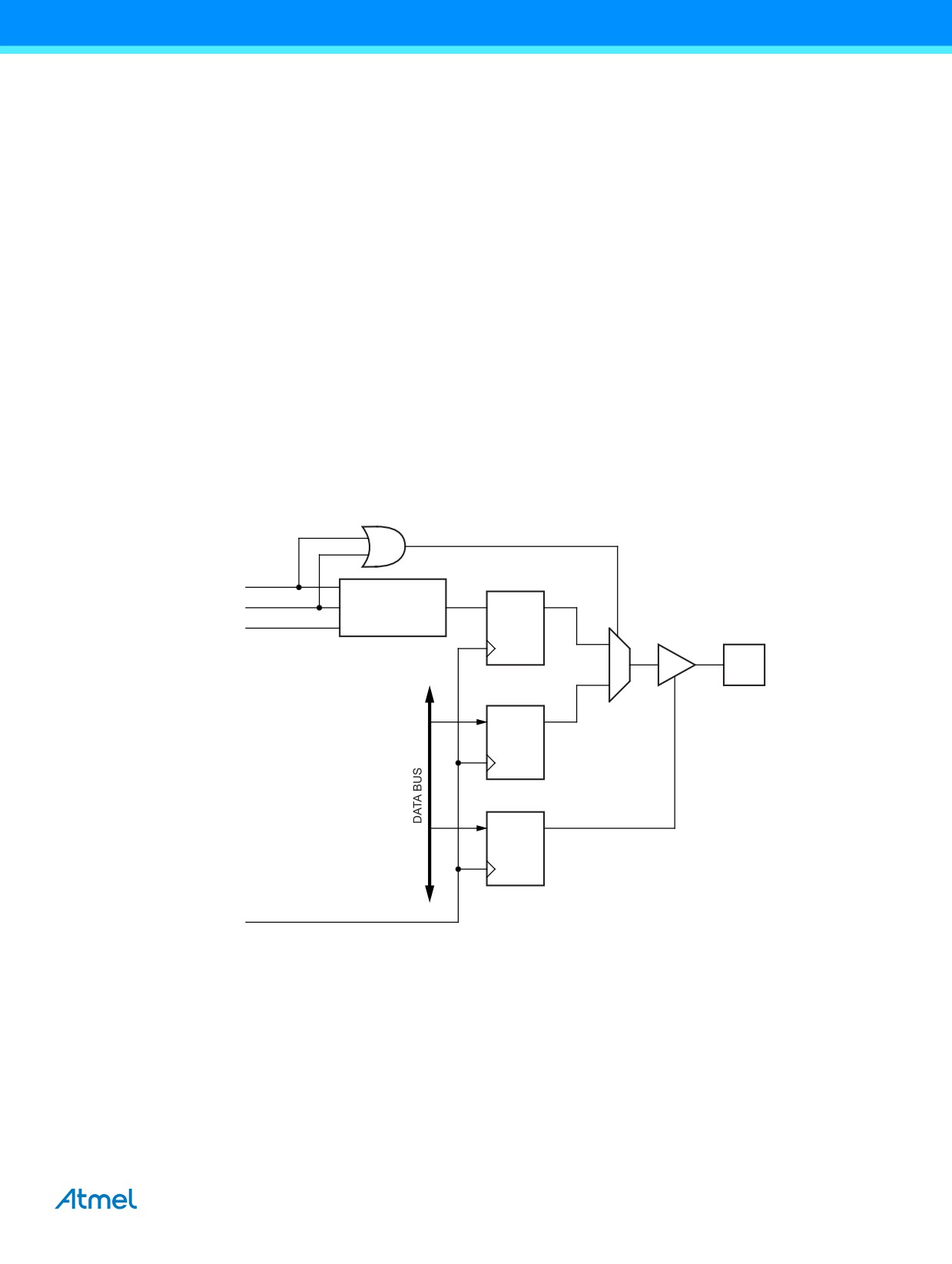
The compare output mode (COM1x1:0) bits have two functions. The waveform generator uses the COM1x1:0 bits for
defining the output compare (OC1x) state at the next compare match. Secondly the COM1x1:0 bits control the OC1x pin
output source. Figure 15-5 shows a simplified schematic of the logic affected by the COM1x1:0 bit setting. The I/O registers,
I/O bits, and I/O pins in the figure are shown in bold. Only the parts of the general I/O port control registers (DDR and PORT)
that are affected by the COM1x1:0 bits are shown. When referring to the OC1x state, the reference is for the internal OC1x
register, not the OC1x pin. If a system reset occur, the OC1x register is reset to “0”.
Figure 15-5. Compare Match Output Unit, Schematic
COMnx1
COMnx0
Waveform
D
Q
Generator
FOCn
1
OCnx
OCnx
Pin
0
D
Q
PORT
D
Q
DDR
clkI/O
The general I/O port function is overridden by the output compare (OC1x) from the waveform generator if either of the
COM1x1:0 bits are set. However, the OC1x pin direction (input or output) is still controlled by the data direction register
(DDR) for the port pin. The data direction register bit for the OC1x pin (DDR_OC1x) must be set as output before the OC1x
value is visible on the pin. The port override function is generally independent of the waveform generation mode, but there
are some exceptions. Refer to Table 15-2 on page 108, Table 15-3 on page 108 and Table 15-4 on page 109 for details.
The design of the output compare pin logic allows initialization of the OC1x state before the output is enabled. Note that
some COM1x1:0 bit settings are reserved for certain modes of operation. See Section 15.11 “Register Description” on page
108. The COM1x1:0 bits have no effect on the input capture unit.
ATmega328P [DATASHEET]
99
7810D-AVR-01/15
15.8.1
Compare Output Mode and Waveform Generation
The waveform generator uses the COM1x1:0 bits differently in normal, CTC, and PWM modes. For all modes, setting the
COM1x1:0 = 0 tells the waveform generator that no action on the OC1x register is to be performed on the next compare
match. For compare output actions in the non-PWM modes refer to Table 15-2 on page 108. For fast PWM mode refer to
Table 15-3 on page 108, and for phase correct and phase and frequency correct PWM refer to Table 15-4 on page 109.
A change of the COM1x1:0 bits state will have effect at the first compare match after the bits are written. For non-PWM
modes, the action can be forced to have immediate effect by using the FOC1x strobe bits.
15.9
Modes of Operation
The mode of operation, i.e., the behavior of the Timer/Counter and the output compare pins, is defined by the combination of
the waveform generation mode (WGM13:0) and compare output mode (COM1x1:0) bits. The compare output mode bits do
not affect the counting sequence, while the waveform generation mode bits do. The COM1x1:0 bits control whether the
PWM output generated should be inverted or not (inverted or non-inverted PWM). For non-PWM modes the COM1x1:0 bits
control whether the output should be set, cleared or toggle at a compare match (see Section 15.8 “Compare Match Output
Unit” on page 99). For detailed timing information refer to Section 15.10 “Timer/Counter Timing Diagrams” on page 106.
15.9.1
Normal Mode
The simplest mode of operation is the normal mode (WGM13:0 = 0). In this mode the counting direction is always up
(incrementing), and no counter clear is performed. The counter simply overruns when it passes its maximum 16-bit value
(MAX = 0xFFFF) and then restarts from the BOTTOM (0x0000). In normal operation the Timer/Counter overflow flag (TOV1)
will be set in the same timer clock cycle as the TCNT1 becomes zero. The TOV1 flag in this case behaves like a 17th bit,
except that it is only set, not cleared. However, combined with the timer overflow interrupt that automatically clears the TOV1
flag, the timer resolution can be increased by software. There are no special cases to consider in the Normal mode, a new
counter value can be written anytime.
The input capture unit is easy to use in normal mode. However, observe that the maximum interval between the external
events must not exceed the resolution of the counter. If the interval between events are too long, the timer overflow interrupt
or the prescaler must be used to extend the resolution for the capture unit.
The output compare units can be used to generate interrupts at some given time. Using the output compare to generate
waveforms in normal mode is not recommended, since this will occupy too much of the CPU time.
15.9.2
Clear Timer on Compare Match (CTC) Mode
In clear timer on compare or CTC mode (WGM13:0 = 4 or 12), the OCR1A or ICR1 register are used to manipulate the
counter resolution. In CTC mode the counter is cleared to zero when the counter value (TCNT1) matches either the OCR1A
(WGM13:0 = 4) or the ICR1 (WGM13:0 = 12). The OCR1A or ICR1 define the top value for the counter, hence also its
resolution. This mode allows greater control of the compare match output frequency. It also simplifies the operation of
counting external events.
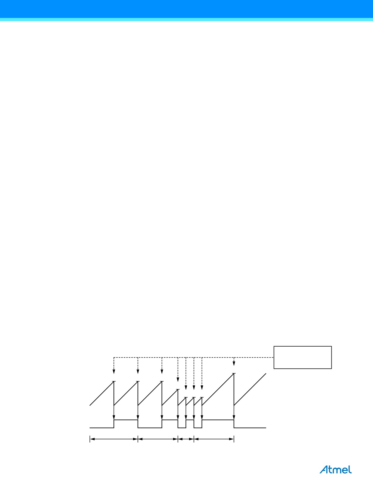
The timing diagram for the CTC mode is shown in Figure 15-6. The counter value (TCNT1) increases until a compare match
occurs with either OCR1A or ICR1, and then counter (TCNT1) is cleared.
Figure 15-6. CTC Mode, Timing Diagram
OCnA Interrupt Flag Set
or ICFn Interrupt Flag Set
(Interrupt on TOP)
TCNTn
OCnA
(COMnA1:0 = 1)
(Toggle)
1
2
3
4
Period
100
ATmega328P [DATASHEET]
7810D-AVR-01/15
An interrupt can be generated at each time the counter value reaches the TOP value by either using the OCF1A or ICF1 flag
according to the register used to define the TOP value. If the interrupt is enabled, the interrupt handler routine can be used
for updating the TOP value. However, changing the TOP to a value close to BOTTOM when the counter is running with none
or a low prescaler value must be done with care since the CTC mode does not have the double buffering feature. If the new
value written to OCR1A or ICR1 is lower than the current value of TCNT1, the counter will miss the compare match. The
counter will then have to count to its maximum value (0xFFFF) and wrap around starting at 0x0000 before the compare
match can occur. In many cases this feature is not desirable. An alternative will then be to use the fast PWM mode using
OCR1A for defining TOP (WGM13:0 = 15) since the OCR1A then will be double buffered.
For generating a waveform output in CTC mode, the OC1A output can be set to toggle its logical level on each compare
match by setting the compare output mode bits to toggle mode (COM1A1:0 = 1). The OC1A value will not be visible on the
port pin unless the data direction for the pin is set to output (DDR_OC1A = 1). The waveform generated will have a
maximum frequency of fOC1A = fclk_I/O/2 when OCR1A is set to zero (0x0000). The waveform frequency is defined by the
following equation:
fclk_I/O
fOCnA
= -----------------------------------------------------
2 N 1 + OCRnA
The N variable represents the prescaler factor (1, 8, 64, 256, or 1024).
As for the normal mode of operation, the TOV1 flag is set in the same timer clock cycle that the counter counts from MAX to
0x0000.
15.9.3
Fast PWM Mode
The fast pulse width modulation or fast PWM mode (WGM13:0 = 5, 6, 7, 14, or 15) provides a high frequency PWM
waveform generation option. The fast PWM differs from the other PWM options by its single-slope operation. The counter
counts from BOTTOM to TOP then restarts from BOTTOM. In non-inverting compare output mode, the output compare
(OC1x) is cleared on the compare match between TCNT1 and OCR1x, and set at BOTTOM. In inverting compare output
mode output is set on compare match and cleared at BOTTOM. Due to the single-slope operation, the operating frequency
of the fast PWM mode can be twice as high as the phase correct and phase and frequency correct PWM modes that use
dual-slope operation. This high frequency makes the fast PWM mode well suited for power regulation, rectification, and DAC
applications. High frequency allows physically small sized external components (coils, capacitors), hence reduces total
system cost.
The PWM resolution for fast PWM can be fixed to 8-, 9-, or 10-bit, or defined by either ICR1 or OCR1A. The minimum
resolution allowed is 2-bit (ICR1 or OCR1A set to 0x0003), and the maximum resolution is 16-bit (ICR1 or OCR1A set to
MAX). The PWM resolution in bits can be calculated by using the following equation:
RFPWM
= ---------------------------------
log2
In fast PWM mode the counter is incremented until the counter value matches either one of the fixed values 0x00FF,
0x01FF, or 0x03FF (WGM13:0 = 5, 6, or 7), the value in ICR1 (WGM13:0 = 14), or the value in OCR1A (WGM13:0 = 15).
The counter is then cleared at the following timer clock cycle. The timing diagram for the fast PWM mode is shown in
Figure 15-7 on page 102. The figure shows fast PWM mode when OCR1A or ICR1 is used to define TOP. The TCNT1 value
is in the timing diagram shown as a histogram for illustrating the single-slope operation. The diagram includes non-inverted
and inverted PWM outputs. The small horizontal line marks on the TCNT1 slopes represent compare matches between
OCR1x and TCNT1. The OC1x interrupt flag will be set when a compare match occurs.
ATmega328P [DATASHEET]
101
7810D-AVR-01/15
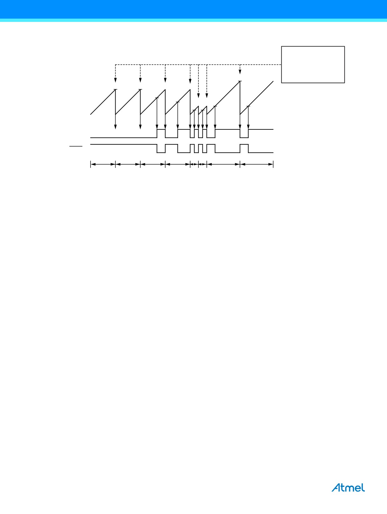
Figure 15-7. Fast PWM Mode, Timing Diagram
OCRnx/ TOP Update and
TOVn Interrupt Flag Set and
OCnA Interrupt Flag Set
or ICFn Interrupt Flag Set
(Interrupt on TOP)
TCNTn
OCnx
(COMnx1:0 = 2)
OCnx
(COMnx1:0 = 3)
1
2
3
4
5
6
7
8
Period
The Timer/Counter overflow flag (TOV1) is set each time the counter reaches TOP. In addition the OC1A or ICF1 flag is set
at the same timer clock cycle as TOV1 is set when either OCR1A or ICR1 is used for defining the TOP value. If one of the
interrupts are enabled, the interrupt handler routine can be used for updating the TOP and compare values.
When changing the TOP value the program must ensure that the new TOP value is higher or equal to the value of all of the
compare registers. If the TOP value is lower than any of the compare registers, a compare match will never occur between
the TCNT1 and the OCR1x. Note that when using fixed TOP values the unused bits are masked to zero when any of the
OCR1x registers are written.
The procedure for updating ICR1 differs from updating OCR1A when used for defining the TOP value. The ICR1 register is
not double buffered. This means that if ICR1 is changed to a low value when the counter is running with none or a low
prescaler value, there is a risk that the new ICR1 value written is lower than the current value of TCNT1. The result will then
be that the counter will miss the compare match at the TOP value. The counter will then have to count to the MAX value
(0xFFFF) and wrap around starting at 0x0000 before the compare match can occur. The OCR1A register however, is double
buffered. This feature allows the OCR1A I/O location to be written anytime. When the OCR1A I/O location is written the
value written will be put into the OCR1A buffer register. The OCR1A compare register will then be updated with the value in
the buffer register at the next timer clock cycle the TCNT1 matches TOP. The update is done at the same timer clock cycle
as the TCNT1 is cleared and the TOV1 flag is set.
Using the ICR1 register for defining TOP works well when using fixed TOP values. By using ICR1, the OCR1A register is
free to be used for generating a PWM output on OC1A. However, if the base PWM frequency is actively changed (by
changing the TOP value), using the OCR1A as TOP is clearly a better choice due to its double buffer feature.
In fast PWM mode, the compare units allow generation of PWM waveforms on the OC1x pins. Setting the COM1x1:0 bits to
two will produce a inverted PWM and an non-inverted PWM output can be generated by setting the COM1x1:0 to three (see
Table on page 108). The actual OC1x value will only be visible on the port pin if the data direction for the port pin is set as
output (DDR_OC1x). The PWM waveform is generated by setting (or clearing) the OC1x register at the compare match
between OCR1x and TCNT1, and clearing (or setting) the OC1x register at the timer clock cycle the counter is cleared
(changes from TOP to BOTTOM).
The PWM frequency for the output can be calculated by the following equation:
fclk_I/O
fOCnxPWM
= -----------------------------------
N 1 + TOP
The N variable represents the prescaler divider (1, 8, 64, 256, or 1024).
The extreme values for the OCR1x register represents special cases when generating a PWM waveform output in the fast
PWM mode. If the OCR1x is set equal to BOTTOM (0x0000) the output will be a narrow spike for each TOP+1 timer clock
cycle. Setting the OCR1x equal to TOP will result in a constant high or low output (depending on the polarity of the output set
by the COM1x1:0 bits.)
102
ATmega328P [DATASHEET]
7810D-AVR-01/15
A frequency (with 50% duty cycle) waveform output in fast PWM mode can be achieved by setting OC1A to toggle its logical
level on each compare match (COM1A1:0 = 1). This applies only if OCR1A is used to define the TOP value
(WGM13:0 = 15). The waveform generated will have a maximum frequency of fOC1A = fclk_I/O/2 when OCR1A is set to zero
(0x0000). This feature is similar to the OC1A toggle in CTC mode, except the double buffer feature of the output compare
unit is enabled in the fast PWM mode.
15.9.4
Phase Correct PWM Mode
The phase correct pulse width modulation or phase correct PWM mode (WGM13:0 = 1, 2, 3, 10, or 11) provides a high
resolution phase correct PWM waveform generation option. The phase correct PWM mode is, like the phase and frequency
correct PWM mode, based on a dual-slope operation. The counter counts repeatedly from BOTTOM (0x0000) to TOP and
then from TOP to BOTTOM. In non-inverting compare output mode, the output compare (OC1x) is cleared on the compare
match between TCNT1 and OCR1x while upcounting, and set on the compare match while downcounting. In inverting output
compare mode, the operation is inverted. The dual-slope operation has lower maximum operation frequency than single
slope operation. However, due to the symmetric feature of the dual-slope PWM modes, these modes are preferred for motor
control applications.
The PWM resolution for the phase correct PWM mode can be fixed to 8-, 9-, or 10-bit, or defined by either ICR1 or OCR1A.
The minimum resolution allowed is 2-bit (ICR1 or OCR1A set to 0x0003), and the maximum resolution is 16-bit (ICR1 or
OCR1A set to MAX). The PWM resolution in bits can be calculated by using the following equation:
RPCPWM
= ---------------------------------
log2
In phase correct PWM mode the counter is incremented until the counter value matches either one of the fixed values
0x00FF, 0x01FF, or 0x03FF (WGM13:0 = 1, 2, or 3), the value in ICR1 (WGM13:0 = 10), or the value in OCR1A
(WGM13:0 = 11). The counter has then reached the TOP and changes the count direction. The TCNT1 value will be equal to
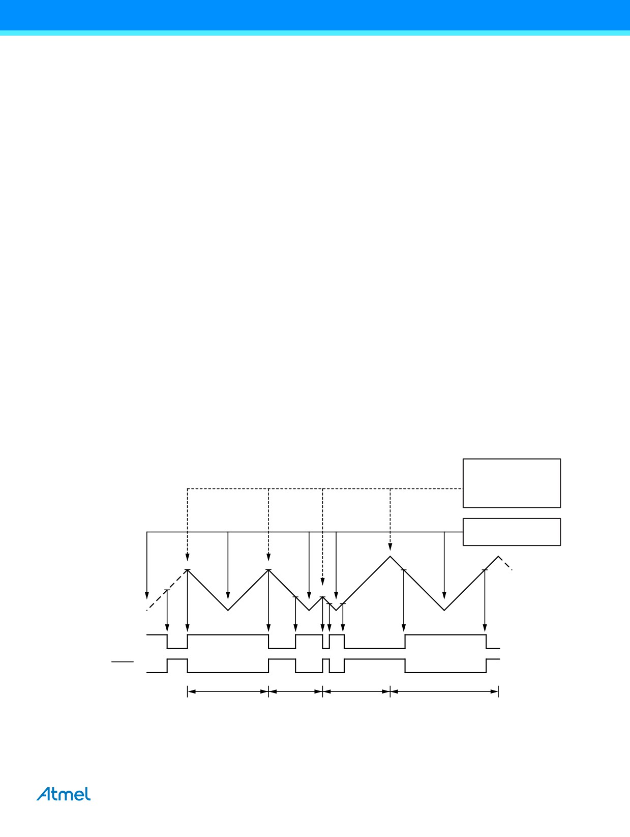
TOP for one timer clock cycle. The timing diagram for the phase correct PWM mode is shown on Figure 15-8. The figure
shows phase correct PWM mode when OCR1A or ICR1 is used to define TOP. The TCNT1 value is in the timing diagram
shown as a histogram for illustrating the dual-slope operation. The diagram includes non-inverted and inverted PWM
outputs. The small horizontal line marks on the TCNT1 slopes represent compare matches between OCR1x and TCNT1.
The OC1x interrupt flag will be set when a compare match occurs.
Figure 15-8. Phase Correct PWM Mode, Timing Diagram
OCRnx/ TOP Update and
OCnA Interrupt Flag Set
or ICFn Interrupt Flag Set
(Interrupt on TOP)
TOVn Interrupt Flag Set
(Interrupt on Bottom)
TCNTn
OCnx
(COMnx1:0 = 2)
OCnx
(COMnx1:0 = 3)
1
2
3
4
Period
The Timer/Counter overflow flag (TOV1) is set each time the counter reaches BOTTOM. When either OCR1A or ICR1 is
used for defining the TOP value, the OC1A or ICF1 flag is set accordingly at the same timer clock cycle as the OCR1x
registers are updated with the double buffer value (at TOP). The interrupt flags can be used to generate an interrupt each
time the counter reaches the TOP or BOTTOM value.
ATmega328P [DATASHEET]
103
7810D-AVR-01/15
When changing the TOP value the program must ensure that the new TOP value is higher or equal to the value of all of the
compare registers. If the TOP value is lower than any of the compare registers, a compare match will never occur between
the TCNT1 and the OCR1x. Note that when using fixed TOP values, the unused bits are masked to zero when any of the
OCR1x registers are written. As the third period shown in Figure 15-8 on page 103 illustrates, changing the TOP actively
while the Timer/Counter is running in the phase correct mode can result in an unsymmetrical output. The reason for this can
be found in the time of update of the OCR1x register. Since the OCR1x update occurs at TOP, the PWM period starts and
ends at TOP. This implies that the length of the falling slope is determined by the previous TOP value, while the length of the
rising slope is determined by the new TOP value. When these two values differ the two slopes of the period will differ in
length. The difference in length gives the unsymmetrical result on the output.
It is recommended to use the phase and frequency correct mode instead of the phase correct mode when changing the TOP
value while the Timer/Counter is running. When using a static TOP value there are practically no differences between the
two modes of operation.
In phase correct PWM mode, the compare units allow generation of PWM waveforms on the OC1x pins. Setting the
COM1x1:0 bits to two will produce a non-inverted PWM and an inverted PWM output can be generated by setting the
COM1x1:0 to three (See Table on page 109). The actual OC1x value will only be visible on the port pin if the data direction
for the port pin is set as output (DDR_OC1x). The PWM waveform is generated by setting (or clearing) the OC1x register at
the compare match between OCR1x and TCNT1 when the counter increments, and clearing (or setting) the OC1x register at
compare match between OCR1x and TCNT1 when the counter decrements. The PWM frequency for the output when using
phase correct PWM can be calculated by the following equation:
fclk_I/O
fOCnxPCPWM
= ------------------------------
2 N TOP
The N variable represents the prescaler divider (1, 8, 64, 256, or 1024).
The extreme values for the OCR1x register represent special cases when generating a PWM waveform output in the phase
correct PWM mode. If the OCR1x is set equal to BOTTOM the output will be continuously low and if set equal to TOP the
output will be continuously high for non-inverted PWM mode. For inverted PWM the output will have the opposite logic
values. If OCR1A is used to define the TOP value (WGM13:0 = 11) and COM1A1:0 = 1, the OC1A output will toggle with a
50% duty cycle.
15.9.5
Phase and Frequency Correct PWM Mode
The phase and frequency correct pulse width modulation, or phase and frequency correct PWM mode (WGM13:0 = 8 or 9)
provides a high resolution phase and frequency correct PWM waveform generation option. The phase and frequency correct
PWM mode is, like the phase correct PWM mode, based on a dual-slope operation. The counter counts repeatedly from
BOTTOM (0x0000) to TOP and then from TOP to BOTTOM. In non-inverting compare output mode, the output compare
(OC1x) is cleared on the compare match between TCNT1 and OCR1x while upcounting, and set on the compare match
while downcounting. In inverting compare output mode, the operation is inverted. The dual-slope operation gives a lower
maximum operation frequency compared to the single-slope operation. However, due to the symmetric feature of the
dual-slope PWM modes, these modes are preferred for motor control applications.
The main difference between the phase correct, and the phase and frequency correct PWM mode is the time the OCR1x
register is updated by the OCR1x buffer register, (see Figure 15-8 on page 103 and Figure 15-9 on page 105).
The PWM resolution for the phase and frequency correct PWM mode can be defined by either ICR1 or OCR1A. The
minimum resolution allowed is 2-bit (ICR1 or OCR1A set to 0x0003), and the maximum resolution is 16-bit (ICR1 or OCR1A
set to MAX). The PWM resolution in bits can be calculated using the following equation:
RPFCPWM
= ---------------------------------
log2
In phase and frequency correct PWM mode the counter is incremented until the counter value matches either the value in
ICR1 (WGM13:0 = 8), or the value in OCR1A (WGM13:0 = 9). The counter has then reached the TOP and changes the
count direction. The TCNT1 value will be equal to TOP for one timer clock cycle. The timing diagram for the phase correct
and frequency correct PWM mode is shown on Figure 15-9 on page 105. The figure shows phase and frequency correct
PWM mode when OCR1A or ICR1 is used to define TOP. The TCNT1 value is in the timing diagram shown as a histogram
for illustrating the dual-slope operation. The diagram includes non-inverted and inverted PWM outputs. The small horizontal
line marks on the TCNT1 slopes represent compare matches between OCR1x and TCNT1. The OC1x interrupt flag will be
set when a compare match occurs.
104
ATmega328P [DATASHEET]
7810D-AVR-01/15
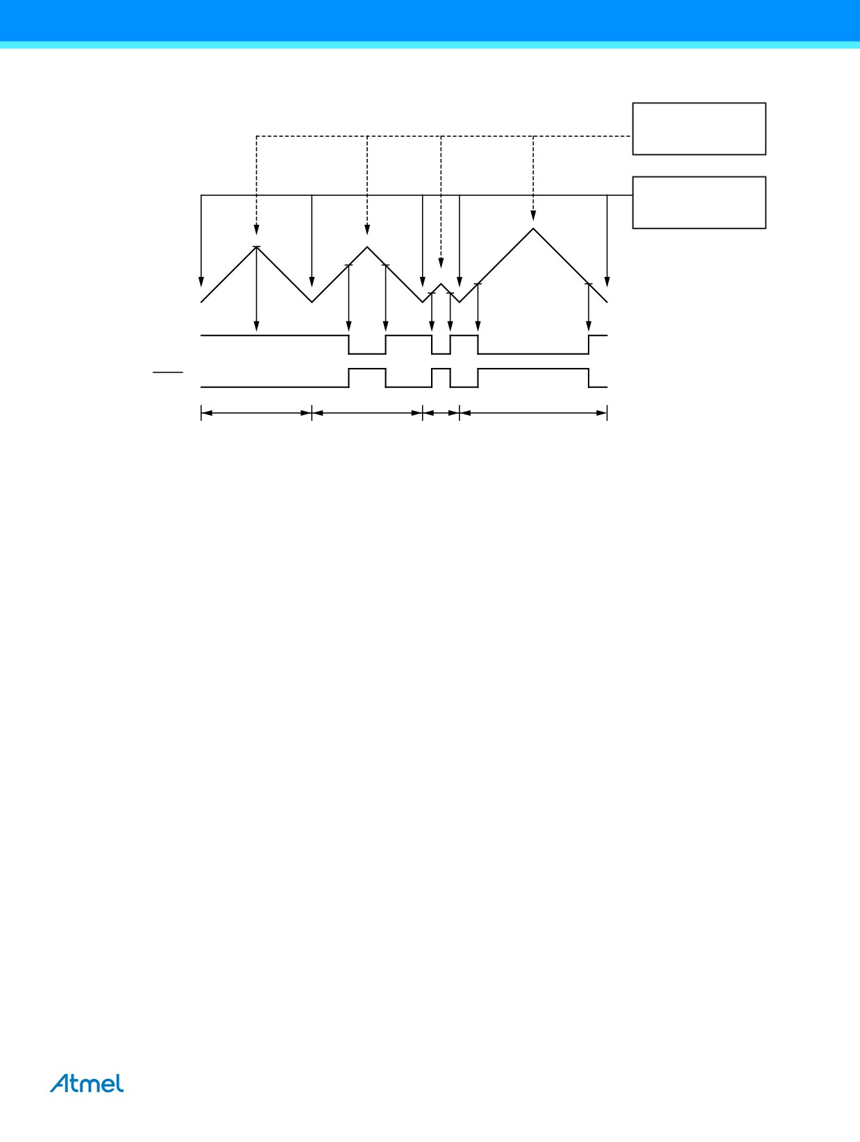
Figure 15-9. Phase and Frequency Correct PWM Mode, Timing Diagram
OCnA Interrupt Flag Set
or ICFn Interrupt Flag Set
(Interrupt on TOP)
OCRnx/ TOP Update and
TOVn Interrupt Flag Set
(Interrupt on Bottom)
TCNTn
(COMnx1:0 = 2)
OCnx
OCnx
(COMnx1:0 = 3)
1
2
3
4
Period
The Timer/Counter overflow flag (TOV1) is set at the same timer clock cycle as the OCR1x registers are updated with the
double buffer value (at BOTTOM). When either OCR1A or ICR1 is used for defining the TOP value, the OC1A or ICF1 flag
set when TCNT1 has reached TOP. The interrupt flags can then be used to generate an interrupt each time the counter
reaches the TOP or BOTTOM value.
When changing the TOP value the program must ensure that the new TOP value is higher or equal to the value of all of the
compare registers. If the TOP value is lower than any of the compare registers, a compare match will never occur between
the TCNT1 and the OCR1x.
As Figure 15-9 shows the output generated is, in contrast to the phase correct mode, symmetrical in all periods. Since the
OCR1x registers are updated at BOTTOM, the length of the rising and the falling slopes will always be equal. This gives
symmetrical output pulses and is therefore frequency correct.
Using the ICR1 register for defining TOP works well when using fixed TOP values. By using ICR1, the OCR1A register is
free to be used for generating a PWM output on OC1A. However, if the base PWM frequency is actively changed by
changing the TOP value, using the OCR1A as TOP is clearly a better choice due to its double buffer feature.
In phase and frequency correct PWM mode, the compare units allow generation of PWM waveforms on the OC1x pins.
Setting the COM1x1:0 bits to two will produce a non-inverted PWM and an inverted PWM output can be generated by setting
the COM1x1:0 to three (See Table on page 109). The actual OC1x value will only be visible on the port pin if the data
direction for the port pin is set as output (DDR_OC1x). The PWM waveform is generated by setting (or clearing) the OC1x
register at the compare match between OCR1x and TCNT1 when the counter increments, and clearing (or setting) the OC1x
register at compare match between OCR1x and TCNT1 when the counter decrements. The PWM frequency for the output
when using phase and frequency correct PWM can be calculated by the following equation:
fclk_I/O
fOCnxPFCPWM
= ------------------------------
2 N TOP
The N variable represents the prescaler divider (1, 8, 64, 256, or 1024).
The extreme values for the OCR1x register represents special cases when generating a PWM waveform output in the phase
correct PWM mode. If the OCR1x is set equal to BOTTOM the output will be continuously low and if set equal to TOP the
output will be set to high for non-inverted PWM mode. For inverted PWM the output will have the opposite logic values. If
OCR1A is used to define the TOP value (WGM13:0 = 9) and COM1A1:0 = 1, the OC1A output will toggle with a 50% duty
cycle.
ATmega328P [DATASHEET]
105
7810D-AVR-01/15
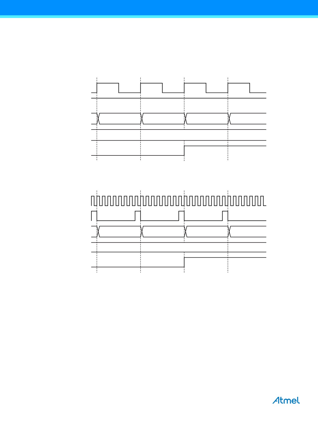
15.10
Timer/Counter Timing Diagrams
The Timer/Counter is a synchronous design and the timer clock (clkT1) is therefore shown as a clock enable signal in the
following figures. The figures include information on when interrupt flags are set, and when the OCR1x register is updated
with the OCR1x buffer value (only for modes utilizing double buffering). Figure 15-10 shows a timing diagram for the setting
of OCF1x.
Figure 15-10. Timer/Counter Timing Diagram, Setting of OCF1x, no Prescaling
clkI/O
clkTn
(clkI/O/1)
TCNTn
OCRnx - 1
OCRnx
OCRnx + 1
OCRnx + 2
OCRnx
OCRnx Value
OCFnx
Figure 15-11 shows the same timing data, but with the prescaler enabled.
Figure 15-11. Timer/Counter Timing Diagram, Setting of OCF1x, with Prescaler (fclk_I/O/8)
clkI/O
clkTn
(clkI/O/8)
TCNTn
OCRnx - 1
OCRnx
OCRnx + 1
OCRnx + 2
OCRnx
OCRnx Value
OCFnx
106
ATmega328P [DATASHEET]
7810D-AVR-01/15
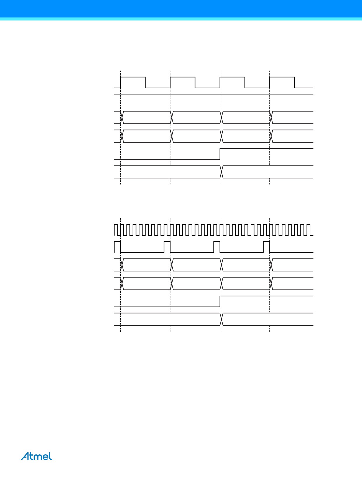
Figure 15-12 shows the count sequence close to TOP in various modes. When using phase and frequency correct PWM
mode the OCR1x register is updated at BOTTOM. The timing diagrams will be the same, but TOP should be replaced by
BOTTOM, TOP-1 by BOTTOM+1 and so on. The same renaming applies for modes that set the TOV1 flag at BOTTOM.
Figure 15-12. Timer/Counter Timing Diagram, no Prescaling
clkI/O
clkTn
(clkI/O/1)
TCNTn
TOP - 1
TOP
BOTTOM
BOTTOM + 1
(CTC and FPWM)
TCNTn
TOP - 1
TOP
TOP -1
TOP -2
(PC and PFC PWM)
TOVn (FPWM)
and ICFn
(if used as TOP)
OCRnx
Old OCRnx Value
New OCRnx Value
(Update at TOP)
Figure 15-13 shows the same timing data, but with the prescaler enabled.
Figure 15-13. Timer/Counter Timing Diagram, with Prescaler (fclk_I/O/8)
clkI/O
clkTn
(clkI/O/8)
TCNTn
TOP - 1
TOP
BOTTOM
BOTTOM + 1
(CTC and FPWM)
TCNTn
(PC and PFC PWM)
TOP - 1
TOP
TOP - 1
TOP - 2
TOVn (FPWM)
and ICFn
(if used as TOP)
OCRnx
Old OCRnx Value
New OCRnx Value
(Update at TOP)
ATmega328P [DATASHEET]
107
7810D-AVR-01/15

15.11
Register Description
15.11.1 TCCR1A - Timer/Counter1 Control Register A
Bit
7
6
5
4
3
2
1
0
(0x80)
COM1A1
COM1A0
COM1B1
COM1B0
-
-
WGM11
WGM10
TCCR1A
Read/Write
R/W
R/W
R/W
R/W
R
R
R/W
R/W
Initial Value
0
0
0
0
0
0
0
0
• Bit 7:6 - COM1A1:0: Compare Output Mode for Channel A
• Bit 5:4 - COM1B1:0: Compare Output Mode for Channel B
The COM1A1:0 and COM1B1:0 control the output compare pins (OC1A and OC1B respectively) behavior. If one or both of
the COM1A1:0 bits are written to one, the OC1A output overrides the normal port functionality of the I/O pin it is connected
to. If one or both of the COM1B1:0 bit are written to one, the OC1B output overrides the normal port functionality of the I/O
pin it is connected to. However, note that the data direction register (DDR) bit corresponding to the OC1A or OC1B pin must
be set in order to enable the output driver.
When the OC1A or OC1B is connected to the pin, the function of the COM1x1:0 bits is dependent of the WGM13:0 bits
setting. Table 15-2 shows the COM1x1:0 bit functionality when the WGM13:0 bits are set to a normal or a CTC mode
(non-PWM).
Table 15-2. Compare Output Mode, non-PWM
COM1A1/COM1B1
COM1A0/COM1B0
Description
0
0
Normal port operation, OC1A/OC1B disconnected.
0
1
Toggle OC1A/OC1B on compare match.
1
0
Clear OC1A/OC1B on compare match (set output to low level).
1
1
Set OC1A/OC1B on compare match (set output to high level).
Table 15-3 shows the COM1x1:0 bit functionality when the WGM13:0 bits are set to the fast PWM mode.
Table 15-3. Compare Output Mode, Fast PWM(1)
COM1A1/COM1B1
COM1A0/COM1B0
Description
0
0
Normal port operation, OC1A/OC1B disconnected.
WGM13:0 = 14 or 15: Toggle OC1A on compare match, OC1B
0
1
disconnected (normal port operation). For all other WGM1
settings, normal port operation, OC1A/OC1B disconnected.
Clear OC1A/OC1B on compare match, set OC1A/OC1B at
1
0
BOTTOM (non-inverting mode)
Set OC1A/OC1B on compare match, clear OC1A/OC1B at
1
1
BOTTOM (inverting mode)
Note:
1.
A special case occurs when OCR1A/OCR1B equals TOP and COM1A1/COM1B1 is set. In this case the
compare match is ignored, but the set or clear is done at BOTTOM. See Section 15.9.3 “Fast PWM Mode” on
page 101 for more details.
108
ATmega328P [DATASHEET]
7810D-AVR-01/15

Table 15-4 shows the COM1x1:0 bit functionality when the WGM13:0 bits are set to the phase correct or the phase and
frequency correct, PWM mode.
Table 15-4. Compare Output Mode, Phase Correct and Phase and Frequency Correct PWM(1)
COM1A1/COM1B1
COM1A0/COM1B0
Description
0
0
Normal port operation, OC1A/OC1B disconnected.
WGM13:0 = 9 or 11: Toggle OC1A on compare match, OC1B
0
1
disconnected (normal port operation). For all other WGM1
settings, normal port operation, OC1A/OC1B disconnected.
Clear OC1A/OC1B on compare match when up-counting. Set
1
0
OC1A/OC1B on compare match when down counting.
Set OC1A/OC1B on compare match when up-counting. Clear
1
1
OC1A/OC1B on compare match when down counting.
Note:
1.
A special case occurs when OCR1A/OCR1B equals TOP and COM1A1/COM1B1 is set. See Section 15.9.4
“Phase Correct PWM Mode” on page 103 for more details.
• Bit 1:0 - WGM11:0: Waveform Generation Mode
Combined with the WGM13:2 bits found in the TCCR1B register, these bits control the counting sequence of the counter, the
source for maximum (TOP) counter value, and what type of waveform generation to be used, see Table 15-5. Modes of
operation supported by the Timer/Counter unit are: Normal mode (counter), clear timer on compare match (CTC) mode, and
three types of pulse width modulation (PWM) modes. See (Section 15.9 “Modes of Operation” on page 100).
Table 15-5. Waveform Generation Mode Bit Description(1)
WGM12
WGM11
WGM10
Timer/Counter Mode of
Update of
TOV1 Flag
Mode
WGM13
(CTC1)
(PWM11)
(PWM10)
Operation
TOP
OCR1x at
Set on
0
0
0
0
0
Normal
0xFFFF
Immediate
MAX
1
0
0
0
1
PWM, phase correct, 8-bit
0x00FF
TOP
BOTTOM
2
0
0
1
0
PWM, phase correct, 9-bit
0x01FF
TOP
BOTTOM
3
0
0
1
1
PWM, phase correct, 10-bit
0x03FF
TOP
BOTTOM
4
0
1
0
0
CTC
OCR1A
Immediate
MAX
5
0
1
0
1
Fast PWM, 8-bit
0x00FF
BOTTOM
TOP
6
0
1
1
0
Fast PWM, 9-bit
0x01FF
BOTTOM
TOP
7
0
1
1
1
Fast PWM, 10-bit
0x03FF
BOTTOM
TOP
PWM, phase and frequency
8
1
0
0
0
ICR1
BOTTOM
BOTTOM
correct
PWM, phase and frequency
9
1
0
0
1
OCR1A
BOTTOM
BOTTOM
correct
10
1
0
1
0
PWM, phase correct
ICR1
TOP
BOTTOM
11
1
0
1
1
PWM, phase correct
OCR1A
TOP
BOTTOM
12
1
1
0
0
CTC
ICR1
Immediate
MAX
13
1
1
0
1
(Reserved)
-
-
-
14
1
1
1
0
Fast PWM
ICR1
BOTTOM
TOP
15
1
1
1
1
Fast PWM
OCR1A
BOTTOM
TOP
Note:
1.
The CTC1 and PWM11:0 bit definition names are obsolete. Use the WGM12:0 definitions. However, the
functionality and location of these bits are compatible with previous versions of the timer.
ATmega328P [DATASHEET]
109
7810D-AVR-01/15
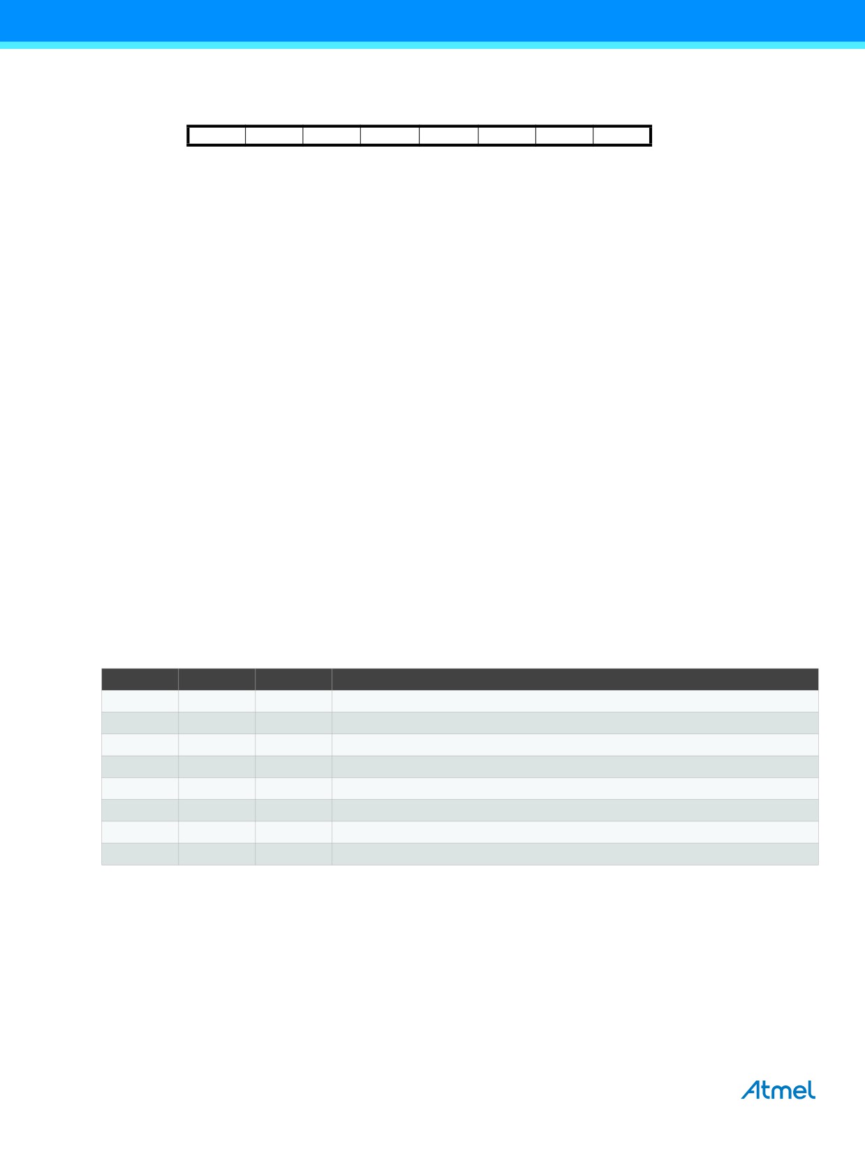
15.11.2 TCCR1B - Timer/Counter1 Control Register B
Bit
7
6
5
4
3
2
1
0
(0x81)
ICNC1
ICES1
-
WGM13
WGM12
CS12
CS11
CS10
TCCR1B
Read/Write
R/W
R/W
R
R/W
R/W
R/W
R/W
R/W
Initial Value
0
0
0
0
0
0
0
0
• Bit 7 - ICNC1: Input Capture Noise Canceler
Setting this bit (to one) activates the input capture noise canceler. When the noise canceler is activated, the input from the
input capture pin (ICP1) is filtered. The filter function requires four successive equal valued samples of the ICP1 pin for
changing its output. The input capture is therefore delayed by four oscillator cycles when the noise canceler is enabled.
• Bit 6 - ICES1: Input Capture Edge Select
This bit selects which edge on the input capture pin (ICP1) that is used to trigger a capture event. When the ICES1 bit is
written to zero, a falling (negative) edge is used as trigger, and when the ICES1 bit is written to one, a rising (positive) edge
will trigger the capture.
When a capture is triggered according to the ICES1 setting, the counter value is copied into the input capture register
(ICR1). The event will also set the input capture flag (ICF1), and this can be used to cause an input capture interrupt, if this
interrupt is enabled.
When the ICR1 is used as TOP value (see description of the WGM13:0 bits located in the TCCR1A and the TCCR1B
register), the ICP1 is disconnected and consequently the input capture function is disabled.
• Bit 5 - Reserved Bit
This bit is reserved for future use. For ensuring compatibility with future devices, this bit must be written to zero when
TCCR1B is written.
• Bit 4:3 - WGM13:2: Waveform Generation Mode
See TCCR1A register description.
• Bit 2:0 - CS12:0: Clock Select
The three clock select bits select the clock source to be used by the Timer/Counter, see Figure 15-10 on page 106 and
Figure 15-11 on page 106.
Table 15-6. Clock Select Bit Description
CS12
CS11
CS10
Description
0
0
0
No clock source (Timer/Counter stopped).
0
0
1
clkI/O/1 (no prescaling)
0
1
0
clkI/O/8 (from prescaler)
0
1
1
clkI/O/64 (from prescaler)
1
0
0
clkI/O/256 (from prescaler)
1
0
1
clkI/O/1024 (from prescaler)
1
1
0
External clock source on T1 pin. Clock on falling edge.
1
1
1
External clock source on T1 pin. Clock on rising edge.
If external pin modes are used for the Timer/Counter1, transitions on the T1 pin will clock the counter even if the pin is
configured as an output. This feature allows software control of the counting.
110
ATmega328P [DATASHEET]
7810D-AVR-01/15
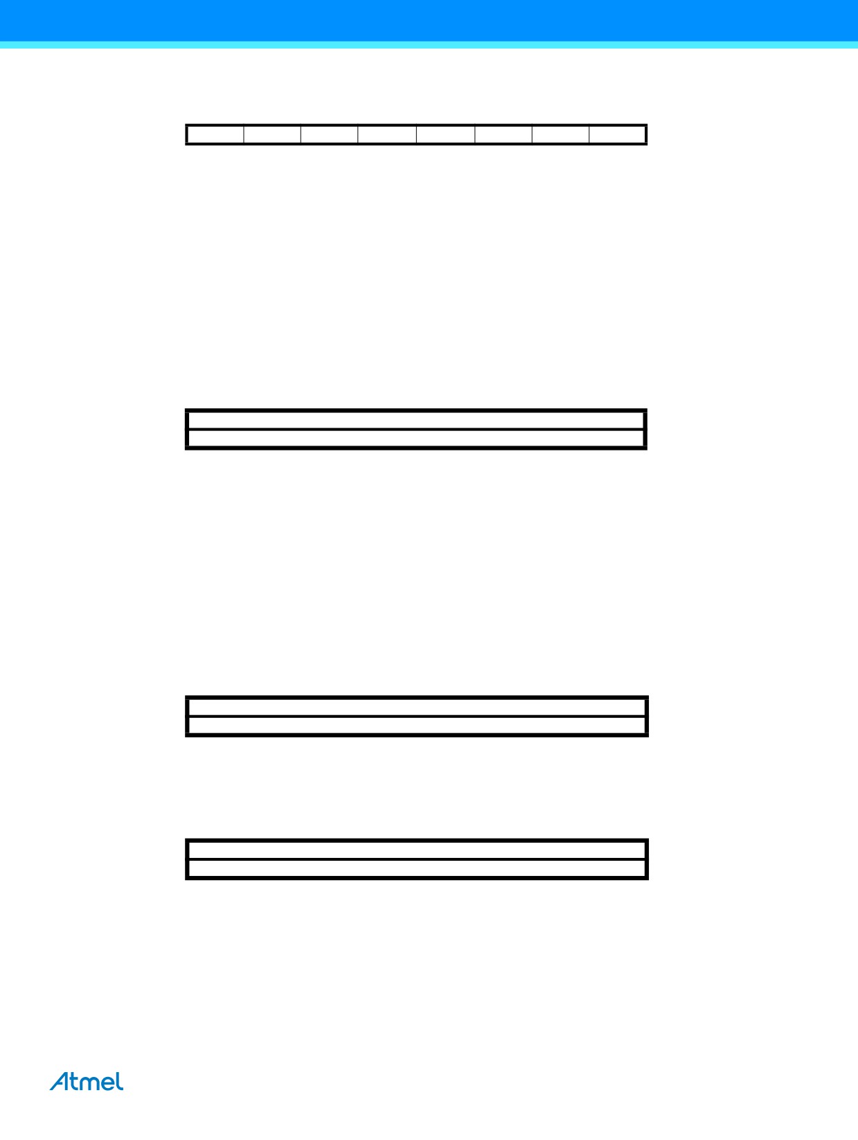
15.11.3 TCCR1C - Timer/Counter1 Control Register C
Bit
7
6
5
4
3
2
1
0
(0x82)
FOC1A
FOC1B
-
-
-
-
-
-
TCCR1C
Read/Write
R/W
R/W
R
R
R
R
R
R
Initial Value
0
0
0
0
0
0
0
0
• Bit 7 - FOC1A: Force Output Compare for Channel A
• Bit 6 - FOC1B: Force Output Compare for Channel B
The FOC1A/FOC1B bits are only active when the WGM13:0 bits specifies a non-PWM mode. When writing a logical one to
the FOC1A/FOC1B bit, an immediate compare match is forced on the waveform generation unit. The OC1A/OC1B output is
changed according to its COM1x1:0 bits setting. Note that the FOC1A/FOC1B bits are implemented as strobes. Therefore it
is the value present in the COM1x1:0 bits that determine the effect of the forced compare.
A FOC1A/FOC1B strobe will not generate any interrupt nor will it clear the timer in clear timer on compare match (CTC)
mode using OCR1A as TOP. The FOC1A/FOC1B bits are always read as zero.
15.11.4 TCNT1H and TCNT1L - Timer/Counter1
Bit
7
6
5
4
3
2
1
0
(0x85)
TCNT1[15:8]
TCNT1H
(0x84)
TCNT1[7:0]
TCNT1L
Read/Write
R/W
R/W
R/W
R/W
R/W
R/W
R/W
R/W
Initial Value
0
0
0
0
0
0
0
0
The two Timer/Counter I/O locations (TCNT1H and TCNT1L, combined TCNT1) give direct access, both for read and for
write operations, to the Timer/Counter unit 16-bit counter. To ensure that both the high and low bytes are read and written
simultaneously when the CPU accesses these registers, the access is performed using an 8-bit temporary high byte register
(TEMP). This temporary register is shared by all the other 16-bit registers. See Section 15.3 “Accessing 16-bit Registers” on
page 91.
Modifying the counter (TCNT1) while the counter is running introduces a risk of missing a compare match between TCNT1
and one of the OCR1x registers.
Writing to the TCNT1 register blocks (removes) the compare match on the following timer clock for all compare units.
15.11.5 OCR1AH and OCR1AL - Output Compare Register 1 A
Bit
7
6
5
4
3
2
1
0
(0x89)
OCR1A[15:8]
OCR1AH
(0x88)
OCR1A[7:0]
OCR1AL
Read/Write
R/W
R/W
R/W
R/W
R/W
R/W
R/W
R/W
Initial Value
0
0
0
0
0
0
0
0
15.11.6 OCR1BH and OCR1BL - Output Compare Register 1 B
Bit
7
6
5
4
3
2
1
0
(0x8B)
OCR1B[15:8]
OCR1BH
(0x8A)
OCR1B[7:0]
OCR1BL
Read/Write
R/W
R/W
R/W
R/W
R/W
R/W
R/W
R/W
Initial Value
0
0
0
0
0
0
0
0
The output compare registers contain a 16-bit value that is continuously compared with the counter value (TCNT1). A match
can be used to generate an output compare interrupt, or to generate a waveform output on the OC1x pin.
The output compare registers are 16-bit in size. To ensure that both the high and low bytes are written simultaneously when
the CPU writes to these registers, the access is performed using an 8-bit temporary high byte register (TEMP). This
temporary register is shared by all the other 16-bit registers. See Section 15.3 “Accessing 16-bit Registers” on page 91.
ATmega328P [DATASHEET]
111
7810D-AVR-01/15
15.11.7 ICR1H and ICR1L - Input Capture Register 1
Bit
7
6
5
4
3
2
1
0
(0x87)
ICR1[15:8]
ICR1H
(0x86)
ICR1[7:0]
ICR1L
Read/Write
R/W
R/W
R/W
R/W
R/W
R/W
R/W
R/W
Initial Value
0
0
0
0
0
0
0
0
The input capture is updated with the counter (TCNT1) value each time an event occurs on the ICP1 pin (or optionally on the
analog comparator output for Timer/Counter1). The input capture can be used for defining the counter TOP value.
The input capture register is 16-bit in size. To ensure that both the high and low bytes are read simultaneously when the
CPU accesses these registers, the access is performed using an 8-bit temporary high byte register (TEMP). This temporary
register is shared by all the other 16-bit registers. See Section 15.3 “Accessing 16-bit Registers” on page 91.
15.11.8 TIMSK1 - Timer/Counter1 Interrupt Mask Register
Bit
7
6
5
4
3
2
1
0
(0x6F)
-
-
ICIE1
-
-
OCIE1B
OCIE1A
TOIE1
TIMSK1
Read/Write
R
R
R/W
R
R
R/W
R/W
R/W
Initial Value
0
0
0
0
0
0
0
0
• Bit 7, 6 - Res: Reserved Bits
These bits are unused bits in the Atmel® ATmega328P, and will always read as zero.
• Bit 5 - ICIE1: Timer/Counter1, Input Capture Interrupt Enable
When this bit is written to one, and the I-flag in the status register is set (interrupts globally enabled), the Timer/Counter1
input capture interrupt is enabled. The corresponding interrupt vector (see Section 11. “Interrupts” on page 49) is executed
when the ICF1 flag, located in TIFR1, is set.
• Bit 4, 3 - Res: Reserved Bits
These bits are unused bits in the Atmel ATmega328P, and will always read as zero.
• Bit 2 - OCIE1B: Timer/Counter1, Output Compare B Match Interrupt Enable
When this bit is written to one, and the I-flag in the status register is set (interrupts globally enabled), the Timer/Counter1
output compare B match interrupt is enabled. The corresponding interrupt vector (see Section 11. “Interrupts” on page 49) is
executed when the OCF1B flag, located in TIFR1, is set.
• Bit 1 - OCIE1A: Timer/Counter1, Output Compare A Match Interrupt Enable
When this bit is written to one, and the I-flag in the status register is set (interrupts globally enabled), the Timer/Counter1
output compare A match interrupt is enabled. The corresponding interrupt vector (see Section 11. “Interrupts” on page 49) is
executed when the OCF1A flag, located in TIFR1, is set.
• Bit 0 - TOIE1: Timer/Counter1, Overflow Interrupt Enable
When this bit is written to one, and the I-flag in the status register is set (interrupts globally enabled), the Timer/Counter1
overflow interrupt is enabled. The corresponding interrupt vector (see Section 11. “Interrupts” on page 49) is executed when
the TOV1 flag, located in TIFR1, is set.
112
ATmega328P [DATASHEET]
7810D-AVR-01/15
15.11.9 TIFR1 - Timer/Counter1 Interrupt Flag Register
Bit
7
6
5
4
3
2
1
0
0x16 (0x36)
-
-
ICF1
-
-
OCF1B
OCF1A
TOV1
TIFR1
Read/Write
R
R
R/W
R
R
R/W
R/W
R/W
Initial Value
0
0
0
0
0
0
0
0
• Bit 7, 6 - Res: Reserved Bits
These bits are unused bits in the Atmel® ATmega328P, and will always read as zero.
• Bit 5 - ICF1: Timer/Counter1, Input Capture Flag
This flag is set when a capture event occurs on the ICP1 pin. When the input capture register (ICR1) is set by the WGM13:0
to be used as the TOP value, the ICF1 flag is set when the counter reaches the TOP value.
ICF1 is automatically cleared when the input capture interrupt vector is executed. Alternatively, ICF1 can be cleared by
writing a logic one to its bit location.
• Bit 4, 3 - Res: Reserved Bits
These bits are unused bits in the Atmel ATmega328P, and will always read as zero.
• Bit 2 - OCF1B: Timer/Counter1, Output Compare B Match Flag
This flag is set in the timer clock cycle after the counter (TCNT1) value matches the output compare register B (OCR1B).
Note that a forced output compare (FOC1B) strobe will not set the OCF1B flag.
OCF1B is automatically cleared when the output compare match B interrupt vector is executed. Alternatively, OCF1B can be
cleared by writing a logic one to its bit location.
• Bit 1 - OCF1A: Timer/Counter1, Output Compare A Match Flag
This flag is set in the timer clock cycle after the counter (TCNT1) value matches the output compare register A (OCR1A).
Note that a forced output compare (FOC1A) strobe will not set the OCF1A flag.
OCF1A is automatically cleared when the output compare match A interrupt vector is executed. Alternatively, OCF1A can be
cleared by writing a logic one to its bit location.
• Bit 0 - TOV1: Timer/Counter1, Overflow Flag
The setting of this flag is dependent of the WGM13:0 bits setting. In normal and CTC modes, the TOV1 flag is set when the
timer overflows. Refer to Table 15-5 on page 109 for the TOV1 flag behavior when using another WGM13:0 bit setting.
TOV1 is automatically cleared when the Timer/Counter1 overflow interrupt vector is executed. Alternatively, TOV1 can be
cleared by writing a logic one to its bit location.
ATmega328P [DATASHEET]
113
7810D-AVR-01/15
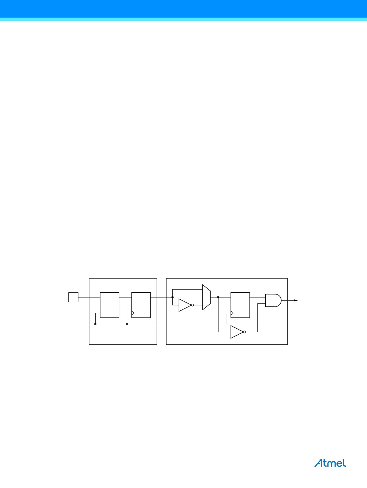
16.
Timer/Counter0 and Timer/Counter1 Prescalers
Section 14. “8-bit Timer/Counter0 with PWM” on page 74 and Section 15. “16-bit Timer/Counter1 with PWM” on page 89
share the same prescaler module, but the Timer/Counters can have different prescaler settings. The description below
applies to both Timer/Counter1 and Timer/Counter0.
16.1
Internal Clock Source
The Timer/Counter can be clocked directly by the system clock (by setting the CSn2:0 = 1). This provides the fastest
operation, with a maximum Timer/Counter clock frequency equal to system clock frequency (fCLK_I/O). Alternatively, one of
four taps from the prescaler can be used as a clock source. The prescaled clock has a frequency of either fCLK_I/O/8,
fCLK_I/O/64, fCLK_I/O/256, or fCLK_I/O/1024.
16.2
Prescaler Reset
The prescaler is free running, i.e., operates independently of the clock select logic of the Timer/Counter, and it is shared by
Timer/Counter1 and Timer/Counter0. Since the prescaler is not affected by the Timer/Counter’s clock select, the state of the
prescaler will have implications for situations where a prescaled clock is used. One example of prescaling artifacts occurs
when the timer is enabled and clocked by the prescaler (6 > CSn2:0 > 1). The number of system clock cycles from when the
timer is enabled to the first count occurs can be from 1 to N+1 system clock cycles, where N equals the prescaler divisor (8,
64, 256, or 1024).
It is possible to use the prescaler reset for synchronizing the Timer/Counter to program execution. However, care must be
taken if the other Timer/Counter that shares the same prescaler also uses prescaling. A prescaler reset will affect the
prescaler period for all Timer/Counters it is connected to.
16.3
External Clock Source
An external clock source applied to the T1/T0 pin can be used as Timer/Counter clock (clkT1/clkT0). The T1/T0 pin is sampled
once every system clock cycle by the pin synchronization logic. The synchronized (sampled) signal is then passed through
the edge detector. Figure 16-1 shows a functional equivalent block diagram of the T1/T0 synchronization and edge detector
logic. The registers are clocked at the positive edge of the internal system clock (clkI/O). The latch is transparent in the high
period of the internal system clock.
The edge detector generates one clkT1/clkT0 pulse for each positive (CSn2:0 = 7) or negative (CSn2:0 = 6) edge it detects.
Figure 16-1. T1/T0 Pin Sampling
Tn_sync
Tn
D
Q
D Q
D Q
(to Clock
Select Logic)
LE
clkI/O
Synchronization
Edge Detector
The synchronization and edge detector logic introduces a delay of 2.5 to 3.5 system clock cycles from an edge has been
applied to the T1/T0 pin to the counter is updated.
Enabling and disabling of the clock input must be done when T1/T0 has been stable for at least one system clock cycle,
otherwise it is a risk that a false Timer/Counter clock pulse is generated.
Each half period of the external clock applied must be longer than one system clock cycle to ensure correct sampling. The
external clock must be guaranteed to have less than half the system clock frequency (fExtClk < fclk_I/O/2) given a 50/50% duty
cycle. Since the edge detector uses sampling, the maximum frequency of an external clock it can detect is half the sampling
frequency (nyquist sampling theorem). However, due to variation of the system clock frequency and duty cycle caused by
oscillator source (crystal, resonator, and capacitors) tolerances, it is recommended that maximum frequency of an external
clock source is less than fclk_I/O/2.5.
An external clock source can not be prescaled.
114
ATmega328P [DATASHEET]
7810D-AVR-01/15
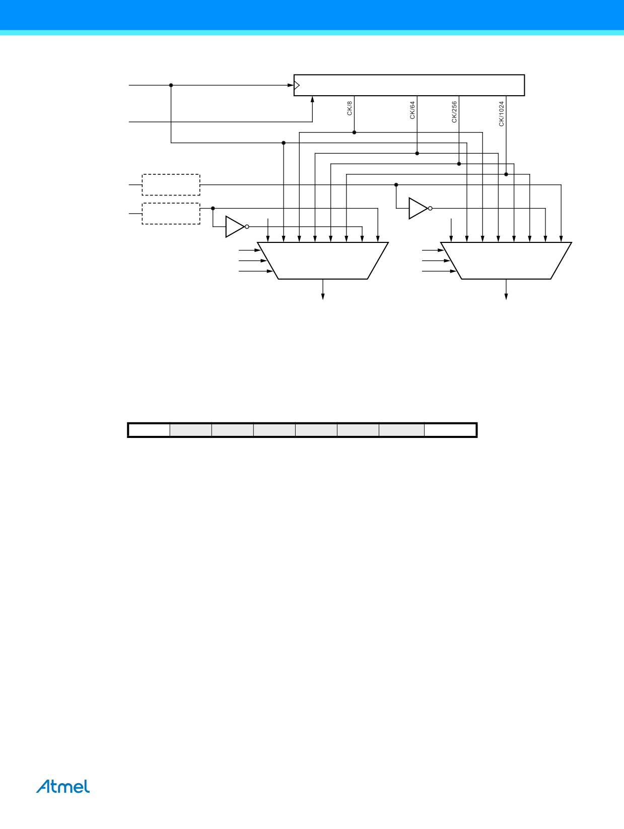
Figure 16-2. Prescaler for Timer/Counter0 and Timer/Counter1(1)
clkI/O
10-bit T/C Prescaler
Clear
PSRSYNC
T0
Synchronization
T1
Synchronization
0
0
CS10
CS00
CS11
CS01
CS12
CS02
Timer/Counter 1Clock Source
Timer/Counter 0 Clock Source
clkT1
clkT0
Note:
1.
The synchronization logic on the input pins (T1/T0) is shown in Figure 16-1.
16.4
Register Description
16.4.1
GTCCR - General Timer/Counter Control Register
Bit
7
6
5
4
3
2
1
0
0x23 (0x43)
TSM
-
-
-
-
-
PSRASY
PSRSYNC
GTCCR
Read/Write
R/W
R
R
R
R
R
R/W
R/W
Initial Value
0
0
0
0
0
0
0
0
• Bit 7 - TSM: Timer/Counter Synchronization Mode
Writing the TSM bit to one activates the Timer/Counter synchronization mode. In this mode, the value that is written to the
PSRASY and PSRSYNC bits is kept, hence keeping the corresponding prescaler reset signals asserted. This ensures that
the corresponding Timer/Counters are halted and can be configured to the same value without the risk of one of them
advancing during configuration. When the TSM bit is written to zero, the PSRASY and PSRSYNC bits are cleared by
hardware, and the Timer/Counters start counting simultaneously.
• Bit 0 - PSRSYNC: Prescaler Reset
When this bit is one, Timer/Counter1 and Timer/Counter0 prescaler will be reset. This bit is normally cleared immediately by
hardware, except if the TSM bit is set. Note that Timer/Counter1 and Timer/Counter0 share the same prescaler and a reset
of this prescaler will affect both timers.
ATmega328P [DATASHEET]
115
7810D-AVR-01/15
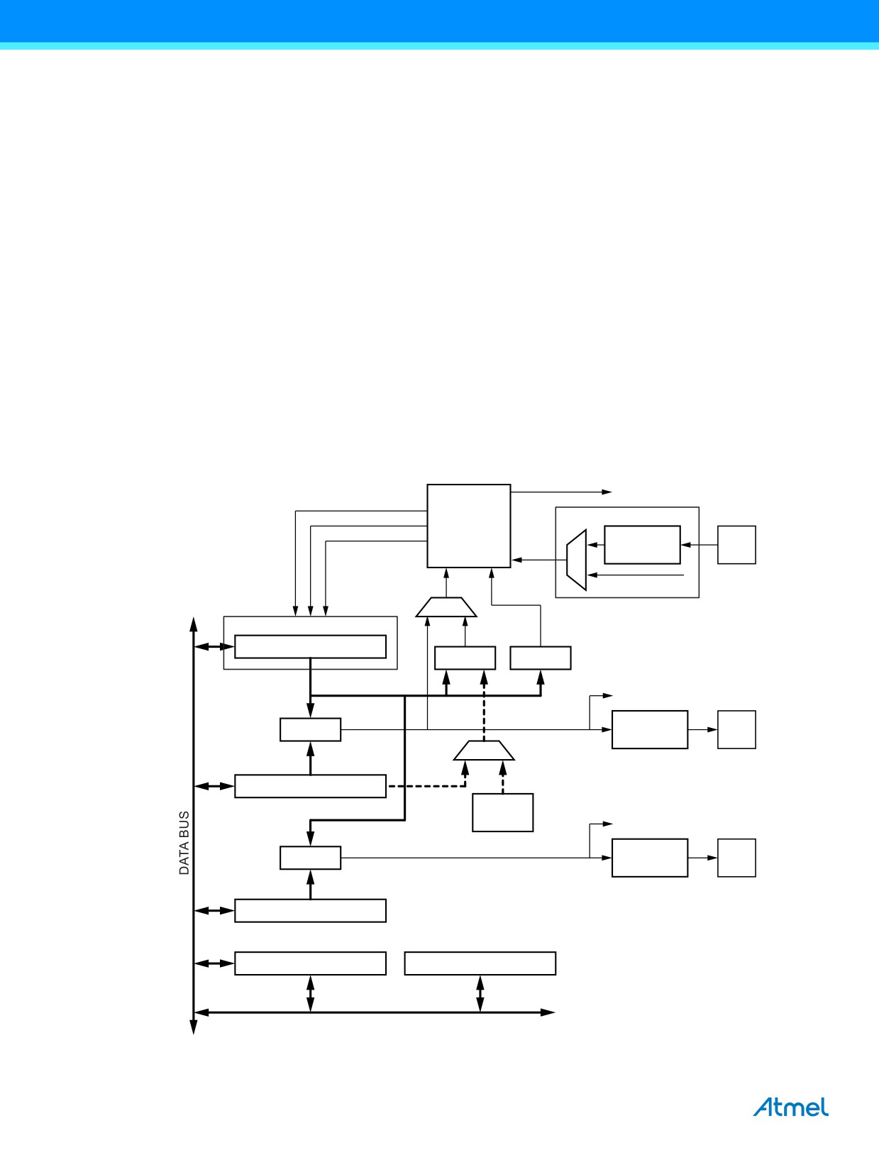
17.
8-bit Timer/Counter2 with PWM and Asynchronous Operation
17.1
Features
● Single channel counter
● Clear timer on compare match (auto reload)
● Glitch-free, phase correct pulse width modulator (PWM)
● Frequency generator
●
10-bit Clock prescaler
● Overflow and compare match interrupt sources (TOV2, OCF2A and OCF2B)
● Allows clocking from external 32kHz watch crystal independent of the I/O clock
17.2
Overview
Timer/Counter2 is a general purpose, single channel, 8-bit Timer/Counter module. A simplified block diagram of the 8-bit
Timer/Counter is shown in Figure 17-1. For the actual placement of I/O pins, refer to Section 1-1 “Pinout” on page 3. CPU
accessible I/O registers, including I/O bits and I/O pins, are shown in bold. The device-specific I/O register and bit locations
are listed in the Section 17.11 “Register Description” on page 127.
The PRTIM2 bit in Section 9.10 “Minimizing Power Consumption” on page 36 must be written to zero to enable
Timer/Counter2 module.
Figure 17-1.
8-bit Timer/Counter Block Diagram
TOVn (Int. Req.)
Count
Clear
Clock Select
Control Logic
Direction
Edge
Tn
clkTn
Detector
(from Prescaler)
TOP
BOTTOM
Timer/Counter
TCNTn
=
= 0
OCnA (Int. Req.)
Waveform
=
OCnA
Generation
OCRnA
Fixed
TOP
Value
OCnB (Int. Req.)
Waveform
OCnB
=
Generation
OCRnB
TCCRnA
TCCRnB
116
ATmega328P [DATASHEET]
7810D-AVR-01/15
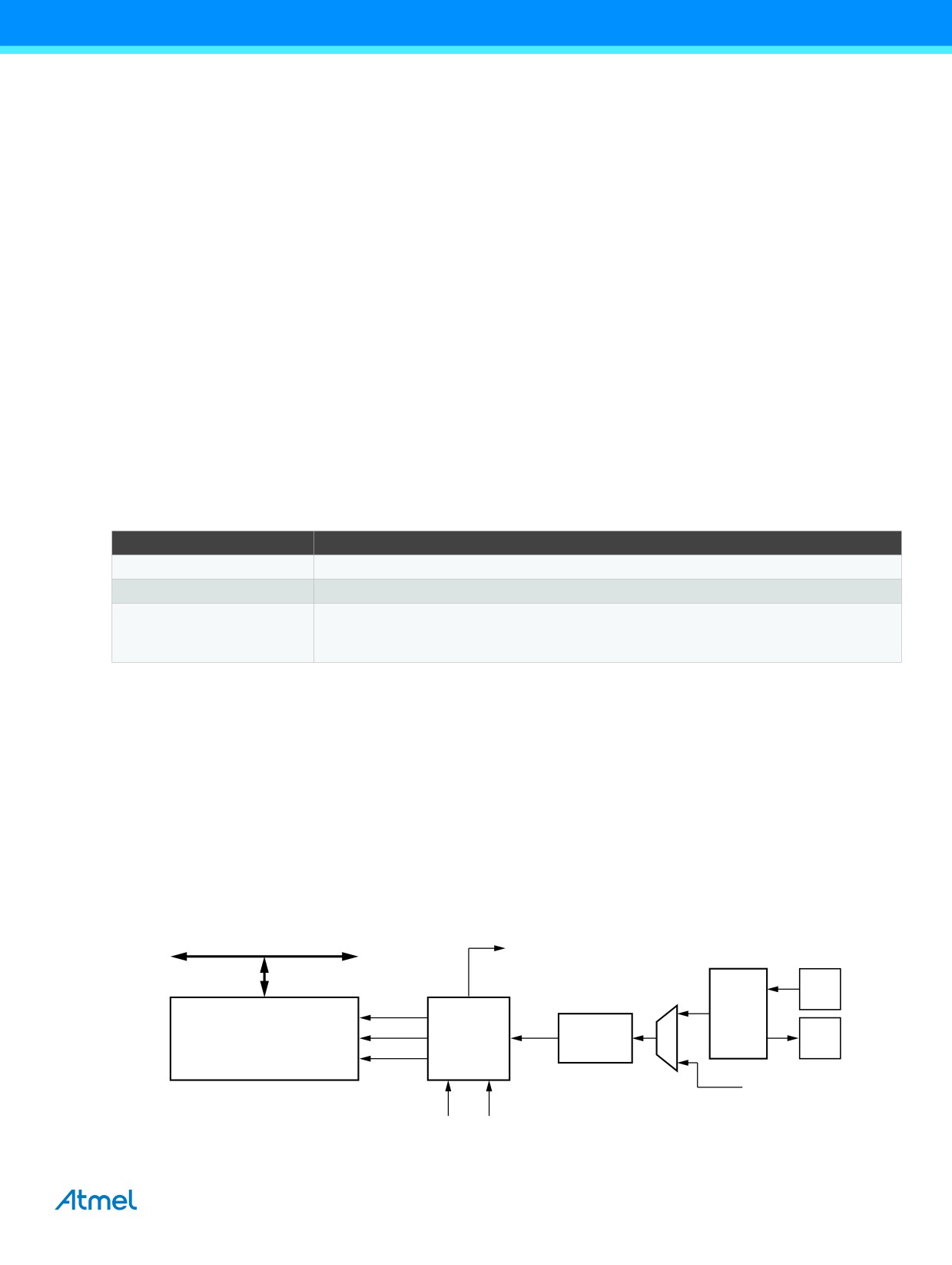
17.2.1
Registers
The Timer/Counter (TCNT2) and output compare register (OCR2A and OCR2B) are 8-bit registers. Interrupt request
(shorten as int.Req.) signals are all visible in the timer interrupt flag register (TIFR2). All interrupts are individually masked
with the timer interrupt mask register (TIMSK2). TIFR2 and TIMSK2 are not shown in the figure.
The Timer/Counter can be clocked internally, via the prescaler, or asynchronously clocked from the TOSC1/2 pins, as
detailed later in this section. The asynchronous operation is controlled by the asynchronous status register (ASSR). The
clock select logic block controls which clock source he Timer/Counter uses to increment (or decrement) its value. The
Timer/Counter is inactive when no clock source is selected. The output from the clock select logic is referred to as the timer
clock (clkT2).
The double buffered output compare register (OCR2A and OCR2B) are compared with the Timer/Counter value at all times.
The result of the compare can be used by the waveform generator to generate a PWM or variable frequency output on the
output compare pins (OC2A and OC2B). See Section 17.5 “Output Compare Unit” on page 118 for details. The compare
match event will also set the compare flag (OCF2A or OCF2B) which can be used to generate an output compare interrupt
request.
17.2.2
Definitions
Many register and bit references in this document are written in general form. A lower case “n” replaces the Timer/Counter
number, in this case 2. However, when using the register or bit defines in a program, the precise form must be used, i.e.,
TCNT2 for accessing Timer/Counter2 counter value and so on.
The definitions in Table 17-1 are also used extensively throughout the section.
Table 17-1. Definitions
Parameter
Definition
BOTTOM
The counter reaches the BOTTOM when it becomes zero (0x00).
MAX
The counter reaches its MAXimum when it becomes 0xFF (decimal 255).
The counter reaches the TOP when it becomes equal to the highest value in the count
TOP
sequence. The TOP value can be assigned to be the fixed value 0xFF (MAX) or the value
stored in the OCR2A register. The assignment is dependent on the mode of operation.
17.3
Timer/Counter Clock Sources
The Timer/Counter can be clocked by an internal synchronous or an external asynchronous clock source. The clock source
clkT2 is by default equal to the MCU clock, clkI/O. When the AS2 bit in the ASSR register is written to logic one, the clock
source is taken from the Timer/Counter oscillator connected to TOSC1 and TOSC2. For details on asynchronous operation,
see Section 17.11.8 “ASSR - Asynchronous Status Register” on page 133. For details on clock sources and prescaler, see
Section 17.10 “Timer/Counter Prescaler” on page 127.
17.4
Counter Unit
The main part of the 8-bit Timer/Counter is the programmable bi-directional counter unit. Figure 17-2 on page 117 shows a
block diagram of the counter and its surrounding environment.
Figure 17-2. Counter Unit Block Diagram
TOVn
DATA BUS
(Int. Req.)
TOSC1
count
T/C
Oscillator
clear
clk
Tn
TCNTn
Control Logic
Prescaler
TOSC2
direction
clkI/O
bottom
top
ATmega328P [DATASHEET]
117
7810D-AVR-01/15
Signal description (internal signals):
count
Increment or decrement TCNT2 by 1.
direction
Selects between increment and decrement.
clear
Clear TCNT2 (set all bits to zero).
clTn
Timer/Counter clock, referred to as clkT2 in the following.
top
Signalizes that TCNT2 has reached maximum value.
bottom
Signalizes that TCNT2 has reached minimum value (zero).
Depending on the mode of operation used, the counter is cleared, incremented, or decremented at each timer clock (clkT2).
clkT2 can be generated from an external or internal clock source, selected by the clock select bits (CS22:0). When no clock
source is selected (CS22:0 = 0) the timer is stopped. However, the TCNT2 value can be accessed by the CPU, regardless of
whether clkT2 is present or not. A CPU write overrides (has priority over) all counter clear or count operations.
The counting sequence is determined by the setting of the WGM21 and WGM20 bits located in the Timer/Counter control
register (TCCR2A) and the WGM22 located in the Timer/Counter control register B (TCCR2B). There are close connections
between how the counter behaves (counts) and how waveforms are generated on the output compare outputs OC2A and
OC2B. For more details about advanced counting sequences and waveform generation, see Section 17.7 “Modes of
Operation” on page 120.
The Timer/Counter overflow flag (TOV2) is set according to the mode of operation selected by the WGM22:0 bits. TOV2 can
be used for generating a CPU interrupt.
17.5
Output Compare Unit
The 8-bit comparator continuously compares TCNT2 with the output compare register (OCR2A and OCR2B). Whenever
TCNT2 equals OCR2A or OCR2B, the comparator signals a match. A match will set the output compare flag (OCF2A or
OCF2B) at the next timer clock cycle. If the corresponding interrupt is enabled, the output compare flag generates an output
compare interrupt. The output compare flag is automatically cleared when the interrupt is executed. Alternatively, the output
compare flag can be cleared by software by writing a logical one to its I/O bit location. The waveform generator uses the
match signal to generate an output according to operating mode set by the WGM22:0 bits and compare output mode
(COM2x1:0) bits. The max and bottom signals are used by the Waveform Generator for handling the special cases of the
extreme values in some modes of operation (Section 17.7 “Modes of Operation” on page 120).
Figure 17-3 shows a block diagram of the output compare unit.
Figure 17-3. Output Compare Unit, Block Diagram
DATA BUS
OCRnx
TCNTn
= (8-bit Comparator)
OCFnx (Int. Req.)
top
bottom
Waveform Generator
OCnx
FOCn
WGMn1:0
COMnx1:0
118
ATmega328P [DATASHEET]
7810D-AVR-01/15
The OCR2x register is double buffered when using any of the pulse width modulation (PWM) modes. For the normal and
clear timer on compare (CTC) modes of operation, the double buffering is disabled. The double buffering synchronizes the
update of the OCR2x compare register to either top or bottom of the counting sequence. The synchronization prevents the
occurrence of odd-length, non-symmetrical PWM pulses, thereby making the output glitch-free.
The OCR2x register access may seem complex, but this is not case. When the double buffering is enabled, the CPU has
access to the OCR2x buffer register, and if double buffering is disabled the CPU will access the OCR2x directly.
17.5.1
Force Output Compare
In non-PWM waveform generation modes, the match output of the comparator can be forced by writing a one to the force
output compare (FOC2x) bit. Forcing compare match will not set the OCF2x flag or reload/clear the timer, but the OC2x pin
will be updated as if a real compare match had occurred (the COM2x1:0 bits settings define whether the OC2x pin is set,
cleared or toggled).
17.5.2
Compare Match Blocking by TCNT2 Write
All CPU write operations to the TCNT2 register will block any compare match that occurs in the next timer clock cycle, even
when the timer is stopped. This feature allows OCR2x to be initialized to the same value as TCNT2 without triggering an
interrupt when the Timer/Counter clock is enabled.
17.5.3
Using the Output Compare Unit
Since writing TCNT2 in any mode of operation will block all compare matches for one timer clock cycle, there are risks
involved when changing TCNT2 when using the output compare channel, independently of whether the Timer/Counter is
running or not. If the value written to TCNT2 equals the OCR2x value, the compare match will be missed, resulting in
incorrect waveform generation. Similarly, do not write the TCNT2 value equal to BOTTOM when the counter is
downcounting.
The setup of the OC2x should be performed before setting the data direction register for the port pin to output. The easiest
way of setting the OC2x value is to use the force output compare (FOC2x) strobe bit in normal mode. The OC2x register
keeps its value even when changing between waveform generation modes.
Be aware that the COM2x1:0 bits are not double buffered together with the compare value. Changing the COM2x1:0 bits will
take effect immediately.
17.6
Compare Match Output Unit
The compare output mode (COM2x1:0) bits have two functions. The waveform generator uses the COM2x1:0 bits for
defining the output compare (OC2x) state at the next compare match. Also, the COM2x1:0 bits control the OC2x pin output
source. Figure 17-4 shows a simplified schematic of the logic affected by the COM2x1:0 bit setting. The I/O registers, I/O
bits, and I/O pins in the figure are shown in bold. Only the parts of the general I/O port control registers (DDR and PORT)
that are affected by the COM2x1:0 bits are shown. When referring to the OC2x state, the reference is for the internal OC2x
register, not the OC2x pin.
ATmega328P [DATASHEET]
119
7810D-AVR-01/15