Atmel ATmega328P 8-bit AVR Microcontroller. DATASHEET (2015) - page 2
10.
System Control and Reset
10.1
Resetting the AVR
During reset, all I/O registers are set to their initial values, and the program starts execution from the reset vector. For the
Atmel® ATmega328P, the instruction placed at the reset vector must be an RJMP - relative jump - instruction to the reset
handling routine. If the program never enables an interrupt source, the interrupt vectors are not used, and regular program
code can be placed at these locations. This is also the case if the reset vector is in the application section while the interrupt
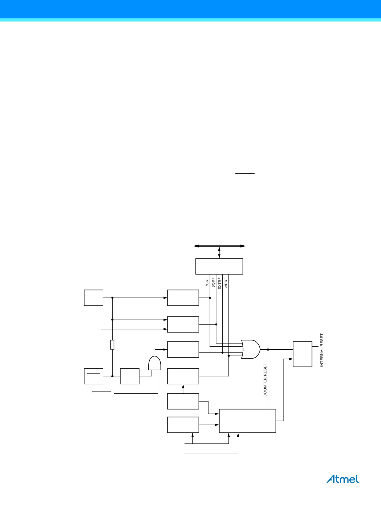
vectors are in the boot section. The circuit diagram in Figure 10-1 shows the reset logic. Table 28-4 on page 261 defines the
electrical parameters of the reset circuitry. The I/O ports of the AVR® are immediately reset to their initial state when a reset
source goes active. This does not require any clock source to be running. After all reset sources have gone inactive, a delay
counter is invoked, stretching the internal reset. This allows the power to reach a stable level before normal operation starts.
The time-out period of the delay counter is defined by the user through the SUT and CKSEL fuses. The different selections
for the delay period are presented in Section 8.2 “Clock Sources” on page 25.
10.2
Reset Sources
The Atmel ATmega328P has four sources of reset:
● Power-on reset. The MCU is reset when the supply voltage is below the power-on reset threshold (VPOT).
● External reset. The MCU is reset when a low level is present on the RESET pin for longer than the minimum pulse
length.
● Watchdog system reset. The MCU is reset when the watchdog timer period expires and the watchdog system reset
mode is enabled.
● Brown-out reset. The MCU is reset when the supply voltage VCC is below the brown-out reset threshold (VBOT) and the
brown-out detector is enabled.
Figure 10-1. Reset Logic
DATA BUS
MCU Status
Register (MCUSR)
Power-on Reset
VCC
Circuit
Brown-out
BODLEVEL [2..0]
Reset Circuit
Pull-up Resistor
Q
Reset Circuit
S
R
SPIKE
Watchdog
RESET
FILTER
Timer
RSTDISBL
Watchdog
Oscillator
Clock
CK
Delay Counters
TIMEOUT
Generator
CKSEL[3:0]
SUT[1:0]
40
ATmega328P [DATASHEET]
7810D-AVR-01/15
10.3
Power-on Reset
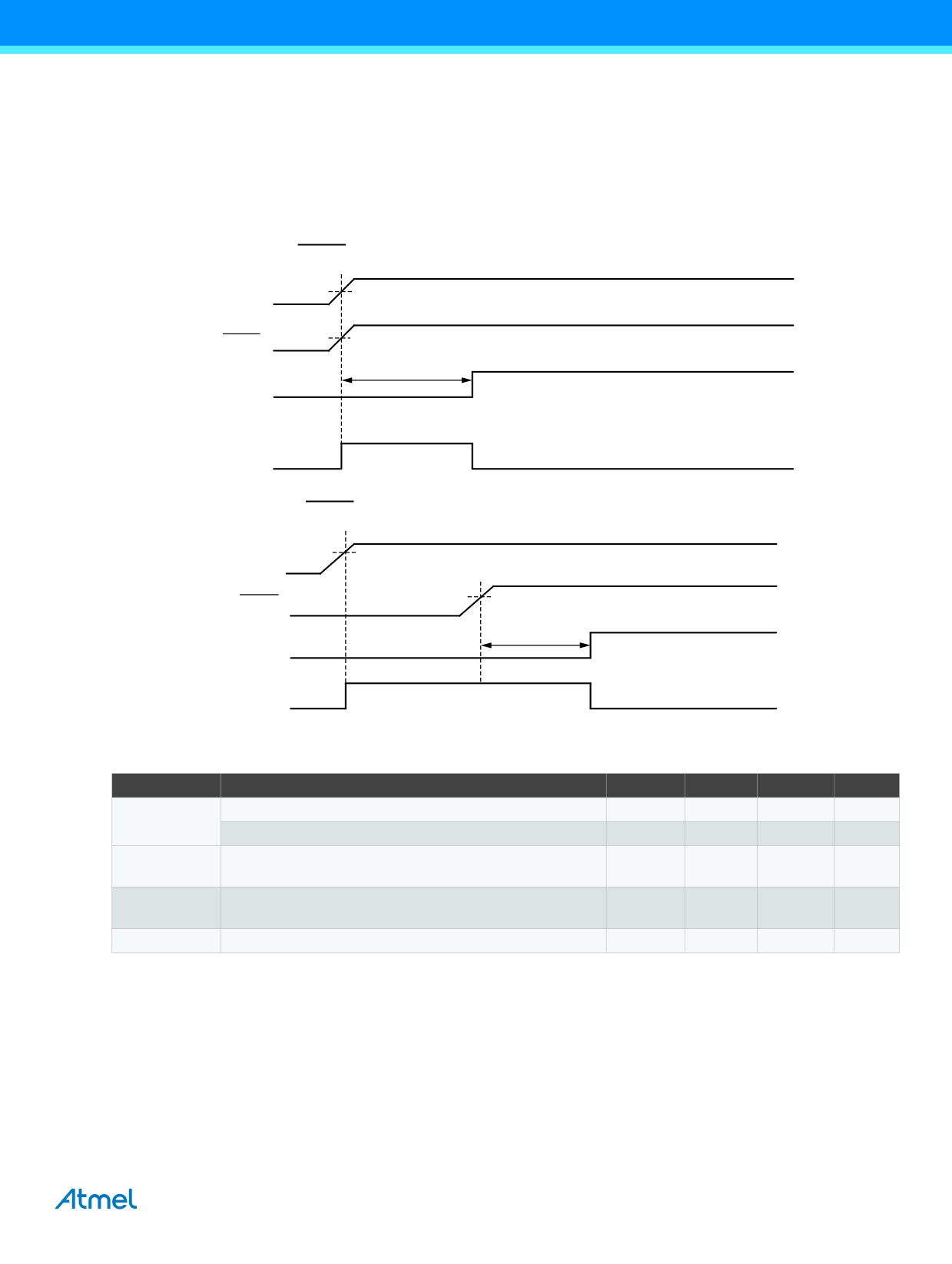
A power-on reset (POR) pulse is generated by an on-chip detection circuit. The detection level is defined in Section 28.6
“System and Reset Characteristics” on page 261. The POR is activated whenever VCC is below the detection level. The POR
circuit can be used to trigger the start-up reset, as well as to detect a failure in supply voltage.
A power-on reset (POR) circuit ensures that the device is reset from power-on. Reaching the power-on reset threshold
voltage invokes the delay counter, which determines how long the device is kept in RESET after VCC rise. The RESET signal
is activated again, without any delay, when VCC decreases below the detection level.
Figure 10-2. MCU Start-up, RESET Tied to VCC
VPOT
VCC
VRST
RESET
tTOUT
Time-out
Internal
Reset
Figure 10-3. . MCU Start-up, RESET Extended Externally
VPOT
VCC
VRST
RESET
t
TOUT
Time-out
Internal
Reset
Table 10-1.
Power On Reset Specifications
Symbol
Parameter
Min
Typ
Max
Units
Power-on reset threshold voltage (rising)
1.4
V
VPOT
Power-on reset threshold voltage (falling)(1)
1.0
1.3
1.6
V
VCC Max. start voltage to ensure internal power-on reset
VPORMAX
0.4
V
signal
VCC Min. start voltage to ensure internal power-on reset
VPORMIN
-0.1
V
signal
VCCRR
VCC rise rate to ensure power-on reset
0.01
V/ms
Note:
1.
Before rising, the supply has to be between VPORMIN and VPORMAX to ensure a reset
ATmega328P [DATASHEET]
41
7810D-AVR-01/15
10.4
External Reset
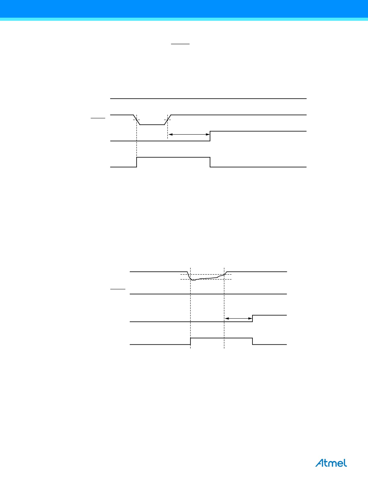
An external reset is generated by a low level on the RESET pin. Reset pulses longer than the minimum pulse width (see
Section 28.6 “System and Reset Characteristics” on page 261) will generate a reset, even if the clock is not running. Shorter
pulses are not guaranteed to generate a reset. When the applied signal reaches the reset threshold voltage - VRST - on its
positive edge, the delay counter starts the MCU after the time-out period - tTOUT - has expired. The external reset can be
disabled by the RSTDISBL fuse, see Table 27-7 on page 244.
Figure 10-4. External Reset During Operation
VCC
VRST
RESET
tTOUT
TIME-OUT
INTERNAL
RESET
10.5
Brown-out Detection
Atmel® ATmega328P has an on-chip brown-out detection (BOD) circuit for monitoring the VCC level during operation by
comparing it to a fixed trigger level. The trigger level for the BOD can be selected by the BODLEVEL fuses. The trigger level
has a hysteresis to ensure spike free brown-out detection. The hysteresis on the detection level should be interpreted as
VBOT+ = VBOT + VHYST/2 and VBOT- = VBOT - VHYST/2.When the BOD is enabled, and VCC decreases to a value below the
trigger level (VBOT- in Figure 10-5), the brown-out reset is immediately activated. When VCC increases above the trigger level
(VBOT+ in Figure 10-5), the delay counter starts the MCU after the time-out period tTOUT has expired.
The BOD circuit will only detect a drop in VCC if the voltage stays below the trigger level for longer than tBOD given in Section
28.6 “System and Reset Characteristics” on page 261.
Figure 10-5. Brown-out Reset During Operation
VCC
VBOT+
VBOT-
RESET
tTOUT
TIME-OUT
INTERNAL
RESET
42
ATmega328P [DATASHEET]
7810D-AVR-01/15
10.6
Watchdog System Reset
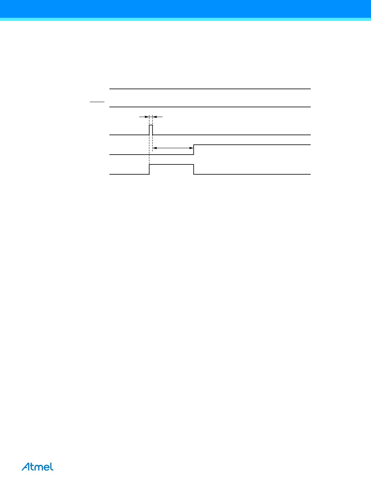
When the watchdog times out, it will generate a short reset pulse of one CK cycle duration. On the falling edge of this pulse,
the delay timer starts counting the time-out period tTOUT. Refer to Section 10.8 “Watchdog Timer” on page 43 for details on
operation of the watchdog timer.
Figure 10-6. Watchdog System Reset During Operation
VCC
RESET
1 CK Cycle
WDT
TIME-OUT
tTOUT
RESET
Time-OUT
INTERNAL
RESET
10.7
Internal Voltage Reference
Atmel® ATmega328P features an internal bandgap reference. This reference is used for brown-out detection, and it can be
used as an input to the analog comparator or the ADC.
10.7.1
Voltage Reference Enable Signals and Start-up Time
The voltage reference has a start-up time that may influence the way it should be used. The start-up time is given in Section
28.6 “System and Reset Characteristics” on page 261. To save power, the reference is not always turned on. The reference
is on during the following situations:
1.
When the BOD is enabled (by programming the BODLEVEL [2:0] Fuses).
2.
When the bandgap reference is connected to the analog comparator (by setting the ACBG bit in ACSR).
3.
When the ADC is enabled.
Thus, when the BOD is not enabled, after setting the ACBG bit or enabling the ADC, the user must always allow the
reference to start up before the output from the analog comparator or ADC is used. To reduce power consumption in
power-down mode, the user can avoid the three conditions above to ensure that the reference is turned off before entering
power-down mode.
10.8
Watchdog Timer
10.8.1
Features
● Clocked from separate on-chip oscillator
●
3 operating modes
● Interrupt
● System reset
● Interrupt and system reset
● Selectable time-out period from 16ms to 8s
● Possible hardware fuse watchdog always on (WDTON) for fail-safe mode
ATmega328P [DATASHEET]
43
7810D-AVR-01/15
10.8.2
Overview
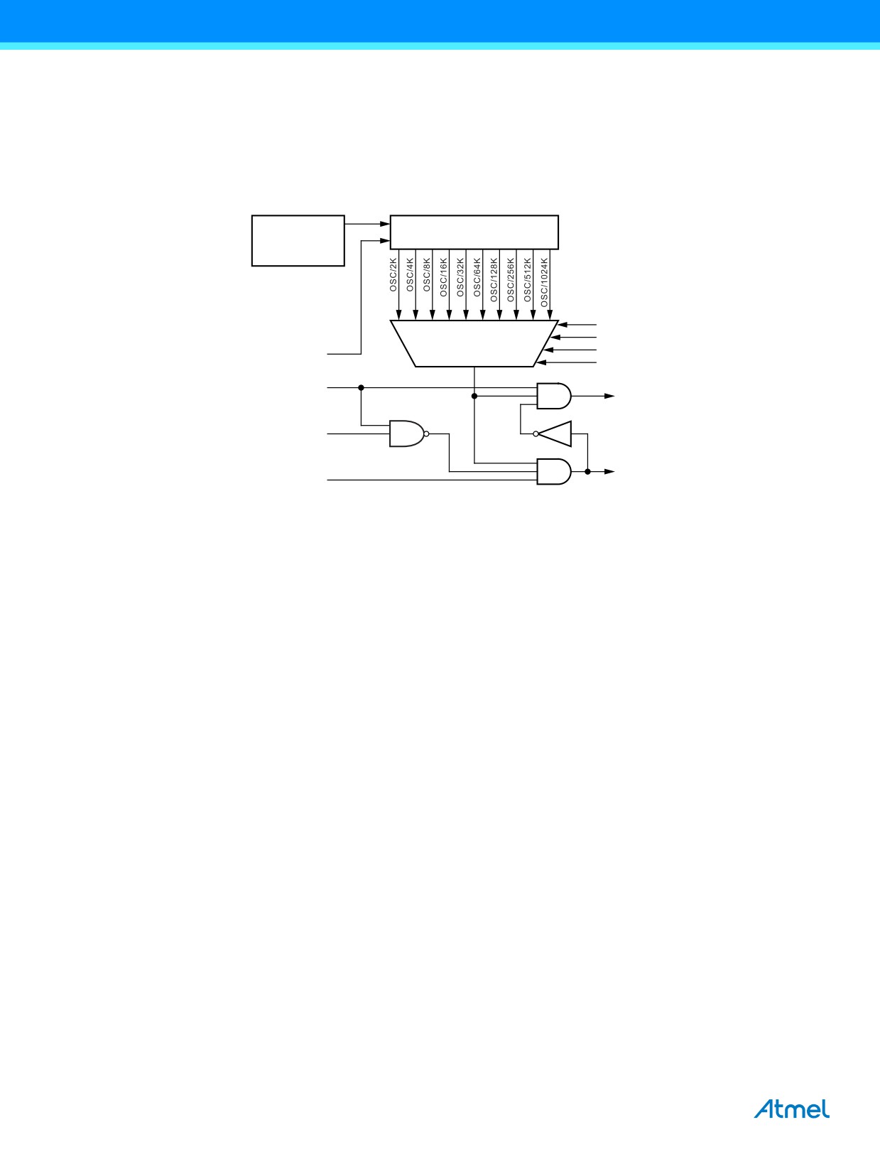
Atmel® ATmega328P has an enhanced watchdog timer (WDT). The WDT is a timer counting cycles of a separate on-chip
128kHz oscillator. The WDT gives an interrupt or a system reset when the counter reaches a given time-out value. In normal
operation mode, it is required that the system uses the WDR - watchdog timer reset - instruction to restart the counter before
the time-out value is reached. If the system doesn't restart the counter, an interrupt or system reset will be issued.
Figure 10-7. Watchdog Timer
Watchdog
128kHz
Prescaler
Oscillator
WDP0
WDP1
WATCHDOG
WDP2
RESET
WDP3
WDE
MCU RESET
WDIF
INTERRUPT
WDIE
In interrupt mode, the WDT gives an interrupt when the timer expires. This interrupt can be used to wake the device from
sleep-modes, and also as a general system timer. One example is to limit the maximum time allowed for certain operations,
giving an interrupt when the operation has run longer than expected. In system reset mode, the WDT gives a reset when the
timer expires. This is typically used to prevent system hang-up in case of runaway code. The third mode, Interrupt and
system reset mode, combines the other two modes by first giving an interrupt and then switch to system reset mode. This
mode will for instance allow a safe shutdown by saving critical parameters before a system reset.
The watchdog always on (WDTON) fuse, if programmed, will force the watchdog timer to system reset mode. With the fuse
programmed the system reset mode bit (WDE) and interrupt mode bit (WDIE) are locked to 1 and 0 respectively. To further
ensure program security, alterations to the watchdog set-up must follow timed sequences.
The sequence for clearing WDE and changing time-out configuration is as follows:
1.
In the same operation, write a logic one to the watchdog change enable bit (WDCE) and WDE. A logic one must
be written to WDE regardless of the previous value of the WDE bit.
2.
Within the next four clock cycles, write the WDE and watchdog prescaler bits (WDP) as desired, but with the
WDCE bit cleared. This must be done in one operation.
44
ATmega328P [DATASHEET]
7810D-AVR-01/15
The following code example shows one assembly and one C function for turning off the watchdog timer. The example
assumes that interrupts are controlled (e.g. by disabling interrupts globally) so that no interrupts will occur during the
execution of these functions.
Assembly Code Example(1)
WDT_off:
; Turn off global interrupt
cli
; Reset Watchdog Timer
wdr
; Clear WDRF in MCUSR
in
r16, MCUSR
andi r16, (0xff & (0<<WDRF))
out
MCUSR, r16
; Write logical one to WDCE and WDE
; Keep old prescaler setting to prevent unintentional time-out
lds r16, WDTCSR
ori
r16, (1<<WDCE) | (1<<WDE)
sts WDTCSR, r16
; Turn off WDT
ldi
r16, (0<<WDE)
sts WDTCSR, r16
; Turn on global interrupt
sei
ret
C Code Example(1)
void WDT_off(void)
{
__disable_interrupt();
__watchdog_reset();
/* Clear WDRF in MCUSR */
MCUSR &= ~(1<<WDRF);
/* Write logical one to WDCE and WDE */
/* Keep old prescaler setting to prevent unintentional time-out
*/
WDTCSR |= (1<<WDCE) | (1<<WDE);
/* Turn off WDT */
WDTCSR = 0x00;
__enable_interrupt();
}
Note:
1.
See Section 5. “About Code Examples” on page 8.
2.
Note: If the watchdog is accidentally enabled, for example by a runaway pointer or brown-out condition, the
device will be reset and the watchdog timer will stay enabled. If the code is not set up to handle the watchdog,
this might lead to an eternal loop of time-out resets. To avoid this situation, the application software should
always clear the watchdog system reset flag (WDRF) and the WDE control bit in the initialization routine, even
if the watchdog is not in use.
ATmega328P [DATASHEET]
45
7810D-AVR-01/15
The following code example shows one assembly and one C function for changing the time-out value of the watchdog timer.
Assembly Code Example(1)
WDT_Prescaler_Change:
; Turn off global interrupt
cli
; Reset Watchdog Timer
wdr
; Start timed sequence
lds r16, WDTCSR
ori
r16, (1<<WDCE) | (1<<WDE)
sts WDTCSR, r16
; -- Got four cycles to set the new values from here -
; Set new prescaler(time-out) value = 64K cycles (~0.5 s)
ldi
r16, (1<<WDE) | (1<<WDP2) | (1<<WDP0)
sts WDTCSR, r16
; -- Finished setting new values, used 2 cycles -
; Turn on global interrupt
sei
ret
C Code Example(1)
void WDT_Prescaler_Change(void)
{
__disable_interrupt();
__watchdog_reset();
/* Start timed equence */
WDTCSR |= (1<<WDCE) | (1<<WDE);
/* Set new prescaler(time-out) value = 64K cycles (~0.5 s) */
WDTCSR = (1<<WDE) | (1<<WDP2) | (1<<WDP0);
__enable_interrupt();
}
Note:
1.
See Section 5. “About Code Examples” on page 8.
2.
The watchdog timer should be reset before any change of the WDP bits, since a change in the WDP bits can
result in a time-out when switching to a shorter time-out period.
10.9
Register Description
10.9.1
MCUSR - MCU Status Register
The MCU status register provides information on which reset source caused an MCU reset.
Bit
7
6
5
4
3
2
1
0
0x35 (0x55)
-
-
-
-
WDRF
BORF
EXTRF
PORF
MCUSR
Read/Write
R
R
R
R
R/W
R/W
R/W
R/W
Initial Value
0
0
0
0
See Bit Description
• Bit 7..4: Res: Reserved Bits
These bits are unused bits in the Atmel® ATmega328P, and will always read as zero.
• Bit 3 - WDRF: Watchdog System Reset Flag
This bit is set if a watchdog system reset occurs. The bit is reset by a power-on reset, or by writing a logic zero to the flag.
• Bit 2 - BORF: Brown-out Reset Flag
This bit is set if a brown-out reset occurs. The bit is reset by a power-on reset, or by writing a logic zero to the flag.
46
ATmega328P [DATASHEET]
7810D-AVR-01/15
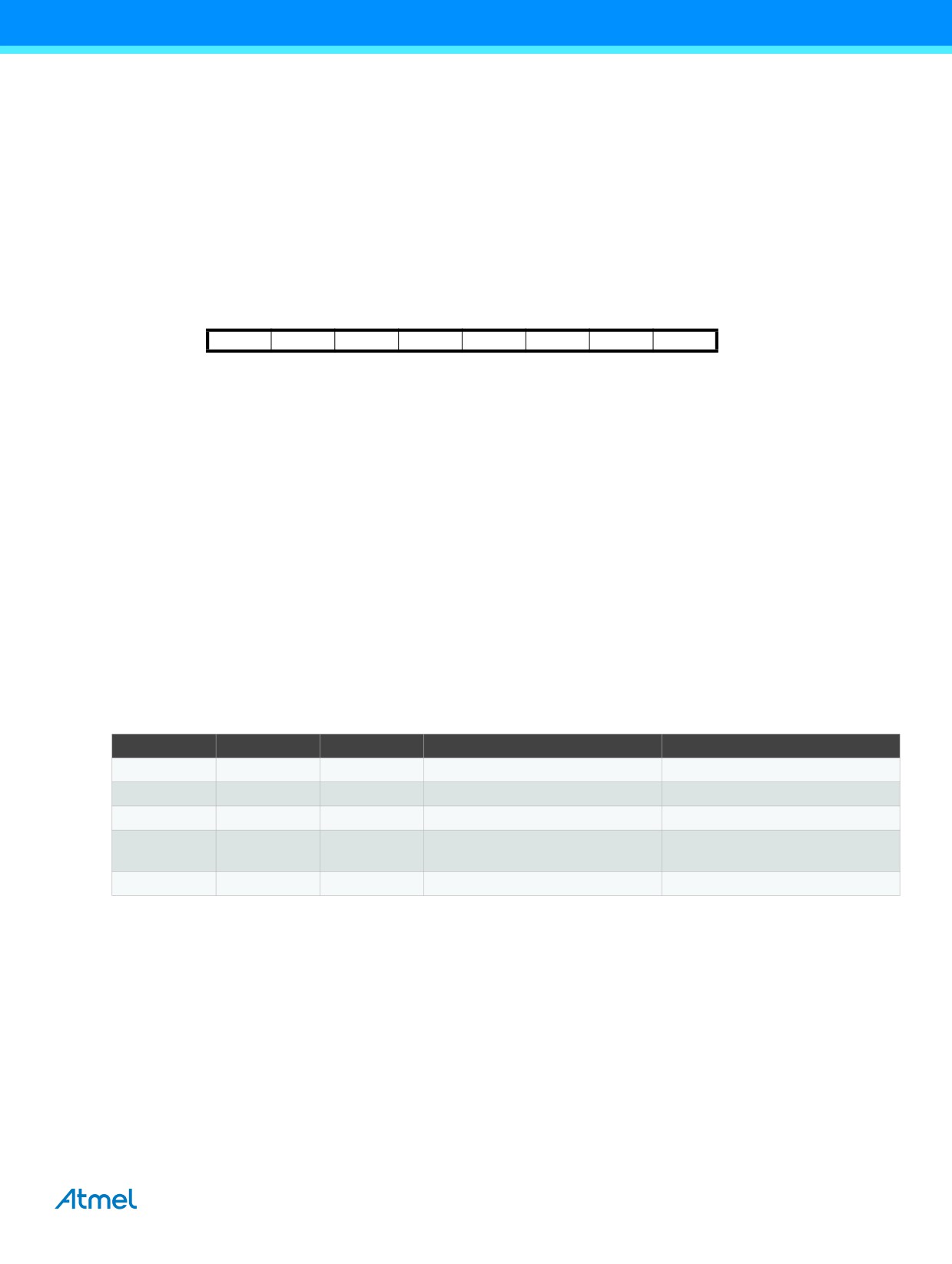
• Bit 1 - EXTRF: External Reset Flag
This bit is set if an external reset occurs. The bit is reset by a power-on reset, or by writing a logic zero to the flag.
• Bit 0 - PORF: Power-on Reset Flag
This bit is set if a power-on reset occurs. The bit is reset only by writing a logic zero to the flag.
To make use of the reset flags to identify a reset condition, the user should read and then reset the MCUSR as early as
possible in the program. If the register is cleared before another reset occurs, the source of the reset can be found by
examining the reset flags.
10.9.2
WDTCSR - Watchdog Timer Control Register
Bit
7
6
5
4
3
2
1
0
(0x60)
WDIF
WDIE
WDP3
WDCE
WDE
WDP2
WDP1
WDP0
WDTCSR
Read/Write
R/W
R/W
R/W
R/W
R/W
R/W
R/W
R/W
Initial Value
0
0
0
0
X
0
0
0
• Bit 7 - WDIF: Watchdog Interrupt Flag
This bit is set when a time-out occurs in the watchdog timer and the watchdog timer is configured for interrupt. WDIF is
cleared by hardware when executing the corresponding interrupt handling vector. Alternatively, WDIF is cleared by writing a
logic one to the flag. When the I-bit in SREG and WDIE are set, the watchdog time-out interrupt is executed.
• Bit 6 - WDIE: Watchdog Interrupt Enable
When this bit is written to one and the I-bit in the status register is set, the watchdog interrupt is enabled. If WDE is cleared in
combination with this setting, the watchdog timer is in interrupt mode, and the corresponding interrupt is executed if time-out
in the watchdog timer occurs. If WDE is set, the watchdog timer is in interrupt and system reset mode. The first time-out in
the watchdog timer will set WDIF.
Executing the corresponding interrupt vector will clear WDIE and WDIF automatically by hardware (the watchdog goes to
system reset mode). This is useful for keeping the watchdog timer security while using the interrupt. To stay in interrupt and
system reset mode, WDIE must be set after each interrupt. This should however not be done within the interrupt service
routine itself, as this might compromise the safety-function of the watchdog system reset mode. If the interrupt is not
executed before the next time-out, a system reset will be applied.
Table 10-2. Watchdog Timer Configuration
WDTON(1)
WDE
WDIE
Mode
Action on Time-out
1
0
0
Stopped
None
1
0
1
Interrupt mode
Interrupt
1
1
0
System reset mode
Reset
Interrupt, then go to system reset
1
1
1
Interrupt and system reset mode
mode
0
x
x
System reset mode
Reset
Note:
1.
WDTON fuse set to “0” means programmed and “1” means unprogrammed.
• Bit 4 - WDCE: Watchdog Change Enable
This bit is used in timed sequences for changing WDE and prescaler bits. To clear the WDE bit, and/or change the prescaler
bits, WDCE must be set.
Once written to one, hardware will clear WDCE after four clock cycles.
ATmega328P [DATASHEET]
47
7810D-AVR-01/15

• Bit 3 - WDE: Watchdog System Reset Enable
WDE is overridden by WDRF in MCUSR. This means that WDE is always set when WDRF is set. To clear WDE, WDRF
must be cleared first. This feature ensures multiple resets during conditions causing failure, and a safe start-up after the
failure.
• Bit 5, 2..0 - WDP3..0: Watchdog Timer Prescaler 3, 2, 1 and 0
The WDP3..0 bits determine the watchdog timer prescaling when the watchdog timer is running. The different prescaling
values and their corresponding time-out periods are shown in Table 10-3.
Table 10-3. Watchdog Timer Prescale Select
WDP3
WDP2
WDP1
WDP0
Number of WDT Oscillator Cycles
Typical Time-out at VCC = 5.0V
0
0
0
0
2K (2048) cycles
16ms
0
0
0
1
4K (4096) cycles
32ms
0
0
1
0
8K (8192) cycles
64ms
0
0
1
1
16K (16384) cycles
0.125s
0
1
0
0
32K (32768) cycles
0.25s
0
1
0
1
64K (65536) cycles
0.5s
0
1
1
0
128K (131072) cycles
1.0s
0
1
1
1
256K (262144) cycles
2.0s
1
0
0
0
512K (524288) cycles
4.0s
1
0
0
1
1024K (1048576) cycles
8.0s
1
0
1
0
1
0
1
1
1
1
0
0
Reserved
1
1
0
1
1
1
1
0
1
1
1
1
48
ATmega328P [DATASHEET]
7810D-AVR-01/15

11.
Interrupts
This section describes the specifics of the interrupt handling as performed in Atmel® ATmega328P. For a general
explanation of the AVR® interrupt handling, refer to Section 6.7 “Reset and Interrupt Handling” on page 15.
● Each interrupt vector occupies two instruction words in Atmel ATmega328P.
● In Atmel ATmega328P, the reset vector is affected by the BOOTRST fuse, and the interrupt vector start address is
affected by the IVSEL bit in MCUCR.
11.1
Interrupt Vectors in ATmega328P
Table 11-1.
Reset and Interrupt Vectors in ATmega328P
Vector No.
Program Address
Source
Interrupt Definition
External pin, power-on reset, brown-out reset and watchdog
1
0x0000
RESET
system reset
2
0x002
INT0
External interrupt request 0
3
0x0004
INT1
External interrupt request 1
4
0x0006
PCINT0
Pin change interrupt request 0
5
0x0008
PCINT1
Pin change interrupt request 1
6
0x000A
PCINT2
Pin change interrupt request 2
7
0x000C
WDT
Watchdog time-out interrupt
8
0x000E
TIMER2 COMPA
Timer/Counter2 compare match A
9
0x0010
TIMER2 COMPB
Timer/Counter2 compare match B
10
0x0012
TIMER2 OVF
Timer/Counter2 overflow
11
0x0014
TIMER1 CAPT
Timer/Counter1 capture event
12
0x0016
TIMER1 COMPA
Timer/Counter1 compare match A
13
0x0018
TIMER1 COMPB
Timer/Counter1 compare match B
14
0x001A
TIMER1 OVF
Timer/Counter1 overflow
15
0x001C
TIMER0 COMPA
Timer/Counter0 compare match A
16
0x001E
TIMER0 COMPB
Timer/Counter0 compare match B
17
0x0020
TIMER0 OVF
Timer/Counter0 overflow
18
0x0022
SPI, STC
SPI serial transfer complete
19
0x0024
USART, RX
USART Rx complete
20
0x0026
USART, UDRE
USART, data register empty
21
0x0028
USART, TX
USART, Tx complete
22
0x002A
ADC
ADC conversion complete
23
0x002C
EE READY
EEPROM ready
24
0x002E
ANALOG COMP
Analog comparator
25
0x0030
TWI
2-wire serial interface
26
0x0032
SPM READY
Store program memory ready
ATmega328P [DATASHEET]
49
7810D-AVR-01/15
Table 11-2 shows reset and interrupt vectors placement for the various combinations of BOOTRST and IVSEL settings. If the
program never enables an interrupt source, the interrupt vectors are not used, and regular program code can be placed at
these locations. This is also the case if the reset vector is in the application section while the interrupt vectors are in the boot
section or vice versa.
Table 11-2. Reset and Interrupt Vectors Placement in ATmega328P(1)
BOOTRST
IVSEL
Reset Address
Interrupt Vectors Start Address
1
0
0x000
0x002
1
1
0x000
Boot reset address + 0x0002
0
0
Boot reset address
0x002
0
1
Boot reset address
Boot reset address + 0x0002
Note:
1.
For the BOOTRST fuse “1” means unprogrammed while “0” means programmed.
The most typical and general program setup for the reset and interrupt vector addresses in Atmel® ATmega328P is:
Address
Labels Code
Comments
0x0000
jmp
RESET
; Reset Handler
0x0002
jmp
EXT_INT0
; IRQ0 Handler
0x0004
jmp
EXT_INT1
; IRQ1 Handler
0x0006
jmp
PCINT0
; PCINT0 Handler
0x0008
jmp
PCINT1
; PCINT1 Handler
0x000A
jmp
PCINT2
; PCINT2 Handler
0x000C
jmp
WDT
; Watchdog Timer Handler
0x000E
jmp
TIM2_COMPA
; Timer2 Compare A Handler
0x0010
jmp
TIM2_COMPB
; Timer2 Compare B Handler
0x0012
jmp
TIM2_OVF
; Timer2 Overflow Handler
0x0014
jmp
TIM1_CAPT
; Timer1 Capture Handler
0x0016
jmp
TIM1_COMPA
; Timer1 Compare A Handler
0x0018
jmp
TIM1_COMPB
; Timer1 Compare B Handler
0x001A
jmp
TIM1_OVF
; Timer1 Overflow Handler
0x001C
jmp
TIM0_COMPA
; Timer0 Compare A Handler
0x001E
jmp
TIM0_COMPB
; Timer0 Compare B Handler
0x0020
jmp
TIM0_OVF
; Timer0 Overflow Handler
0x0022
jmp
SPI_STC
; SPI Transfer Complete Handler
0x0024
jmp
USART_RXC
; USART, RX Complete Handler
0x0026
jmp
USART_UDRE
; USART, UDR Empty Handler
0x0028
jmp
USART_TXC
; USART, TX Complete Handler
0x002A
jmp
ADC
; ADC Conversion Complete Handler
0x002C
jmp
EE_RDY
; EEPROM Ready Handler
0x002E
jmp
ANA_COMP
; Analog Comparator Handler
0x0030
jmp
TWI
; 2-wire Serial Interface Handler
0x0032
jmp
SPM_RDY
; Store Program Memory Ready Handler
;
0x0033
RESET: ldi
r16, high(RAMEND); Main program start
0x0034
out
SPH,r16
; Set Stack Pointer to top of RAM
0x0035
ldi
r16, low(RAMEND)
0x0036
out
SPL,r16
0x0037
sei
; Enable interrupts
0x0038
<instr> xxx
50
ATmega328P [DATASHEET]
7810D-AVR-01/15
When the BOOTRST fuse is unprogrammed, the boot section size set to 2Kbytes and the IVSEL bit in the MCUCR register
is set before any interrupts are enabled, the most typical and general program setup for the reset and interrupt vector
addresses in Atmel® ATmega328P is:
Address
Labels Code
Comments
0x0000
RESET: ldi
r16,high(RAMEND); Main program start
0x0001
out
SPH,r16
; Set Stack Pointer to top of RAM
0x0002
ldi
r16,low(RAMEND)
0x0003
out
SPL,r16
0x0004
sei
; Enable interrupts
0x0005
<instr> xxx
;
.org 0x3C02
0x3C02
jmp
EXT_INT0
; IRQ0 Handler
0x3C04
jmp
EXT_INT1
; IRQ1 Handler
;
0x3C32
jmp
SPM_RDY
; Store Program Memory Ready Handler
When the BOOTRST fuse is programmed and the boot section size set to 2Kbytes, the most typical and general program
setup for the reset and interrupt vector addresses in Atmel ATmega328P is:
Address
Labels Code
Comments
.org 0x0002
0x0002
jmp
EXT_INT0
; IRQ0 Handler
0x0004
jmp
EXT_INT1
; IRQ1 Handler
;
0x0032
jmp
SPM_RDY
; Store Program Memory Ready Handler
;
.org 0x3C00
0x3C00
RESET: ldi
r16,high(RAMEND); Main program start
0x3C01
out
SPH,r16
; Set Stack Pointer to top of RAM
0x3C02
ldi
r16,low(RAMEND)
0x3C03
out
SPL,r16
0x3C04
sei
; Enable interrupts
0x3C05
<instr> xxx
When the BOOTRST fuse is programmed, the boot section size set to 2Kbytes and the IVSEL bit in the MCUCR register is
set before any interrupts are enabled, the most typical and general program setup for the reset and interrupt vector
addresses in Atmel ATmega328P is:
Address
Labels Code
Comments
;
.org 0x3C00
0x3C00
jmp
RESET
; Reset handler
0x3C02
jmp
EXT_INT0
; IRQ0 Handler
0x3C04
jmp
EXT_INT1
; IRQ1 Handler
;
0x3C32
jmp
SPM_RDY
; Store Program Memory Ready Handler
;
0x3C33
RESET: ldi
r16,high(RAMEND); Main program start
0x3C34
out
SPH,r16
; Set Stack Pointer to top of RAM
0x3C35
ldi
r16,low(RAMEND)
0x3C36
out
SPL,r16
0x3C37
sei
; Enable interrupts
0x3C38
<instr> xxx
ATmega328P [DATASHEET]
51
7810D-AVR-01/15

11.2
Register Description
11.2.1
Moving Interrupts Between Application and Boot Space
The MCU control register controls the placement of the interrupt vector table.
11.2.2
MCUCR - MCU Control Register
Bit
7
6
5
4
3
2
1
0
0x35 (0x55)
-
BODS
BODSE
PUD
-
-
IVSEL
IVCE
MCUCR
Read/Write
R
R
R
R/W
R
R
R/W
R/W
Initial Value
0
0
0
0
0
0
0
0
• Bit 1 - IVSEL: Interrupt Vector Select
When the IVSEL bit is cleared (zero), the interrupt vectors are placed at the start of the flash memory. When this bit is set
(one), the interrupt vectors are moved to the beginning of the boot loader section of the flash. The actual address of the start
of the boot flash section is determined by the BOOTSZ fuses. Refer to the Section 26. “Boot Loader Support - Read-While-
Write Self-Programming” on page 229 for details. To avoid unintentional changes of interrupt vector tables, a special write
procedure must be followed to change the IVSEL bit:
a. Write the interrupt vector change enable (IVCE) bit to one.
b. Within four cycles, write the desired value to IVSEL while writing a zero to IVCE.
Interrupts will automatically be disabled while this sequence is executed. Interrupts are disabled in the cycle IVCE is set, and
they remain disabled until after the instruction following the write to IVSEL. If IVSEL is not written, interrupts remain disabled
for four cycles. The I-bit in the status register is unaffected by the automatic disabling.
Note:
If interrupt vectors are placed in the boot loader section and boot lock bit BLB02 is programmed, interrupts are
disabled while executing from the application section. If interrupt vectors are placed in the application section
and boot lock bit BLB12 is programed, interrupts are disabled while executing from the boot loader section.
Refer to the Section 26. “Boot Loader Support - Read-While-Write Self-Programming” on page 229 for details
on boot lock bits.
This bit is not available in Atmel® ATmega328P.
• Bit 0 - IVCE: Interrupt Vector Change Enable
The IVCE bit must be written to logic one to enable change of the IVSEL bit. IVCE is cleared by hardware four cycles after it
is written or when IVSEL is written. Setting the IVCE bit will disable interrupts, as explained in the IVSEL description above.
See code example below.
Assembly Code Example
Move_interrupts:
; Enable change of Interrupt Vectors
ldi
r16, (1<<IVCE)
out
MCUCR, r16
; Move interrupts to Boot Flash section
ldi
r16, (1<<IVSEL)
out
MCUCR, r16
ret
C Code Example
void Move_interrupts(void)
{
/* Enable change of Interrupt Vectors */
MCUCR = (1<<IVCE);
/* Move interrupts to Boot Flash section */
MCUCR = (1<<IVSEL);
}
This bit is not available in Atmel ATmega328P.
52
ATmega328P [DATASHEET]
7810D-AVR-01/15
12.
External Interrupts
The external interrupts are triggered by the INT0 and INT1 pins or any of the PCINT23..0 pins. Observe that, if enabled, the
interrupts will trigger even if the INT0 and INT1 or PCINT23..0 pins are configured as outputs. This feature provides a way of
generating a software interrupt. The pin change interrupt PCI2 will trigger if any enabled PCINT23..16 pin toggles. The pin
change interrupt PCI1 will trigger if any enabled PCINT14..8 pin toggles. The pin change interrupt PCI0 will trigger if any
enabled PCINT7..0 pin toggles. The PCMSK2, PCMSK1 and PCMSK0 registers control which pins contribute to the pin
change interrupts. Pin change interrupts on PCINT23..0 are detected asynchronously. This implies that these interrupts can
be used for waking the part also from sleep modes other than Idle mode.
The INT0 and INT1 interrupts can be triggered by a falling or rising edge or a low level. This is set up as indicated in the
specification for the external interrupt control register A - EICRA. When the INT0 or INT1 interrupts are enabled and are
configured as level triggered, the interrupts will trigger as long as the pin is held low. Note that recognition of falling or rising
edge interrupts on INT0 or INT1 requires the presence of an I/O clock, described in Section 8.1 “Clock Systems and their
Distribution” on page 24. Low level interrupt on INT0 and INT1 is detected asynchronously. This implies that this interrupt
can be used for waking the part also from sleep modes other than idle mode. The I/O clock is halted in all sleep modes
except Idle mode.
Note that if a level triggered interrupt is used for wake-up from power-down, the required level must be held long enough for
the MCU to complete the wake-up to trigger the level interrupt. If the level disappears before the end of the start-up time, the
MCU will still wake up, but no interrupt will be generated. The start-up time is defined by the SUT and CKSEL fuses as
described in Section 8. “System Clock and Clock Options” on page 24.
12.1
Pin Change Interrupt Timing
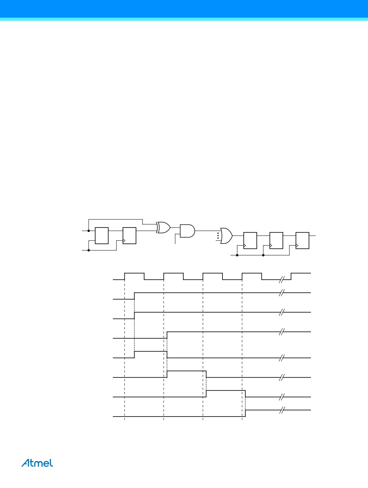
An example of timing of a pin change interrupt is shown in Figure 12-1.
Figure 12-1. Timing of Pin Change Interrupts
pin_lat
pin_sync
pcint_in_(0)
0
pcint_sync
pcint_setflag
PCINT(0)
D Q
PCIF
LE
x
PCINT(0) in PCMSK(x)
clk
clk
clk
PCINT(0)
pin_lat
pin_sync
pcint_in_(0)
pcint_syn
pcint_setflag
PCIF
ATmega328P [DATASHEET]
53
7810D-AVR-01/15

12.2
Register Description
12.2.1
EICRA - External Interrupt Control Register A
The external interrupt control register A contains control bits for interrupt sense control.
Bit
7
6
5
4
3
2
1
0
(0x69)
-
-
-
-
ISC11
ISC10
ISC01
ISC00
EICRA
Read/Write
R
R
R
R
R/W
R/W
R/W
R/W
Initial Value
0
0
0
0
0
0
0
0
• Bit 7..4 - Res: Reserved Bits
These bits are unused bits in the Atmel® ATmega328P, and will always read as zero.
• Bit 3, 2 - ISC11, ISC10: Interrupt Sense Control 1 Bit 1 and Bit 0
The external interrupt 1 is activated by the external pin INT1 if the SREG I-flag and the corresponding interrupt mask are set.
The level and edges on the external INT1 pin that activate the interrupt are defined in Table 12-1. The value on the INT1 pin
is sampled before detecting edges. If edge or toggle interrupt is selected, pulses that last longer than one clock period will
generate an interrupt. Shorter pulses are not guaranteed to generate an interrupt. If low level interrupt is selected, the low
level must be held until the completion of the currently executing instruction to generate an interrupt.
Table 12-1. Interrupt 1 Sense Control
ISC11
ISC10
Description
0
0
The low level of INT1 generates an interrupt request.
0
1
Any logical change on INT1 generates an interrupt request.
1
0
The falling edge of INT1 generates an interrupt request.
1
1
The rising edge of INT1 generates an interrupt request.
• Bit 1, 0 - ISC01, ISC00: Interrupt Sense Control 0 Bit 1 and Bit 0
The external interrupt 0 is activated by the external pin INT0 if the SREG I-flag and the corresponding interrupt mask are set.
The level and edges on the external INT0 pin that activate the interrupt are defined in Table 12-2. The value on the INT0 pin
is sampled before detecting edges. If edge or toggle interrupt is selected, pulses that last longer than one clock period will
generate an interrupt. Shorter pulses are not guaranteed to generate an interrupt. If low level interrupt is selected, the low
level must be held until the completion of the currently executing instruction to generate an interrupt.
Table 12-2. Interrupt 0 Sense Control
ISC01
ISC00
Description
0
0
The low level of INT0 generates an interrupt request.
0
1
Any logical change on INT0 generates an interrupt request.
1
0
The falling edge of INT0 generates an interrupt request.
1
1
The rising edge of INT0 generates an interrupt request.
54
ATmega328P [DATASHEET]
7810D-AVR-01/15
12.2.2
EIMSK - External Interrupt Mask Register
Bit
7
6
5
4
3
2
1
0
0x1D (0x3D)
-
-
-
-
-
-
INT1
INT0
EIMSK
Read/Write
R
R
R
R
R
R
R/W
R/W
Initial Value
0
0
0
0
0
0
0
0
• Bit 7..2 - Res: Reserved Bits
These bits are unused bits in the Atmel® ATmega328P, and will always read as zero.
• Bit 1 - INT1: External Interrupt Request 1 Enable
When the INT1 bit is set (one) and the I-bit in the status register (SREG) is set (one), the external pin interrupt is enabled.
The interrupt sense control1 bits 1/0 (ISC11 and ISC10) in the external interrupt control register A (EICRA) define whether
the external interrupt is activated on rising and/or falling edge of the INT1 pin or level sensed. Activity on the pin will cause an
interrupt request even if INT1 is configured as an output. The corresponding interrupt of external interrupt request 1 is
executed from the INT1 interrupt vector.
• Bit 0 - INT0: External Interrupt Request 0 Enable
When the INT0 bit is set (one) and the I-bit in the status register (SREG) is set (one), the external pin interrupt is enabled.
The interrupt sense control0 bits 1/0 (ISC01 and ISC00) in the external interrupt control register A (EICRA) define whether
the external interrupt is activated on rising and/or falling edge of the INT0 pin or level sensed. Activity on the pin will cause an
interrupt request even if INT0 is configured as an output. The corresponding interrupt of external interrupt request 0 is
executed from the INT0 interrupt vector.
12.2.3
EIFR - External Interrupt Flag Register
Bit
7
6
5
4
3
2
1
0
0x1C (0x3C)
-
-
-
-
-
-
INTF1
INTF0
EIFR
Read/Write
R
R
R
R
R
R
R/W
R/W
Initial Value
0
0
0
0
0
0
0
0
• Bit 7..2 - Res: Reserved Bits
These bits are unused bits in the Atmel ATmega328P, and will always read as zero.
• Bit 1 - INTF1: External Interrupt Flag 1
When an edge or logic change on the INT1 pin triggers an interrupt request, INTF1 becomes set (one). If the I-bit in SREG
and the INT1 bit in EIMSK are set (one), the MCU will jump to the corresponding interrupt vector. The flag is cleared when
the interrupt routine is executed. Alternatively, the flag can be cleared by writing a logical one to it. This flag is always cleared
when INT1 is configured as a level interrupt.
• Bit 0 - INTF0: External Interrupt Flag 0
When an edge or logic change on the INT0 pin triggers an interrupt request, INTF0 becomes set (one). If the I-bit in SREG
and the INT0 bit in EIMSK are set (one), the MCU will jump to the corresponding interrupt vector. The flag is cleared when
the interrupt routine is executed. Alternatively, the flag can be cleared by writing a logical one to it. This flag is always cleared
when INT0 is configured as a level interrupt.
ATmega328P [DATASHEET]
55
7810D-AVR-01/15
12.2.4
PCICR - Pin Change Interrupt Control Register
Bit
7
6
5
4
3
2
1
0
(0x68)
-
-
-
-
-
PCIE2
PCIE1
PCIE0
PCICR
Read/Write
R
R
R
R
R
R/W
R/W
R/W
Initial Value
0
0
0
0
0
0
0
0
• Bit 7..3 - Res: Reserved Bits
These bits are unused bits in the Atmel® ATmega328P, and will always read as zero.
• Bit 2 - PCIE2: Pin Change Interrupt Enable 2
When the PCIE2 bit is set (one) and the I-bit in the status register (SREG) is set (one), pin change interrupt 2 is enabled. Any
change on any enabled PCINT23..16 pin will cause an interrupt. The corresponding interrupt of pin change interrupt request
is executed from the PCI2 interrupt vector. PCINT23..16 pins are enabled individually by the PCMSK2 register.
• Bit 1 - PCIE1: Pin Change Interrupt Enable 1
When the PCIE1 bit is set (one) and the I-bit in the status register (SREG) is set (one), pin change interrupt 1 is enabled. Any
change on any enabled PCINT14..8 pin will cause an interrupt. The corresponding interrupt of pin change interrupt request is
executed from the PCI1 interrupt vector. PCINT14..8 pins are enabled individually by the PCMSK1 register.
• Bit 0 - PCIE0: Pin Change Interrupt Enable 0
When the PCIE0 bit is set (one) and the I-bit in the status register (SREG) is set (one), pin change interrupt 0 is enabled. Any
change on any enabled PCINT7..0 pin will cause an interrupt. The corresponding interrupt of pin change interrupt request is
executed from the PCI0 interrupt vector. PCINT7..0 pins are enabled individually by the PCMSK0 register.
12.2.5
PCIFR - Pin Change Interrupt Flag Register
Bit
7
6
5
4
3
2
1
0
0x1B (0x3B)
-
-
-
-
-
PCIF2
PCIF1
PCIF0
PCIFR
Read/Write
R
R
R
R
R
R/W
R/W
R/W
Initial Value
0
0
0
0
0
0
0
0
• Bit 7..3 - Res: Reserved Bits
These bits are unused bits in the Atmel ATmega328P, and will always read as zero.
• Bit 2 - PCIF2: Pin Change Interrupt Flag 2
When a logic change on any PCINT23..16 pin triggers an interrupt request, PCIF2 becomes set (one). If the I-bit in SREG
and the PCIE2 bit in PCICR are set (one), the MCU will jump to the corresponding interrupt vector. The flag is cleared when
the interrupt routine is executed. Alternatively, the flag can be cleared by writing a logical one to it.
• Bit 1 - PCIF1: Pin Change Interrupt Flag 1
When a logic change on any PCINT14..8 pin triggers an interrupt request, PCIF1 becomes set (one). If the I-bit in SREG and
the PCIE1 bit in PCICR are set (one), the MCU will jump to the corresponding interrupt vector. The flag is cleared when the
interrupt routine is executed. Alternatively, the flag can be cleared by writing a logical one to it.
• Bit 0 - PCIF0: Pin Change Interrupt Flag 0
When a logic change on any PCINT7..0 pin triggers an interrupt request, PCIF0 becomes set (one). If the I-bit in SREG and
the PCIE0 bit in PCICR are set (one), the MCU will jump to the corresponding interrupt vector. The flag is cleared when the
interrupt routine is executed. Alternatively, the flag can be cleared by writing a logical one to it.
56
ATmega328P [DATASHEET]
7810D-AVR-01/15
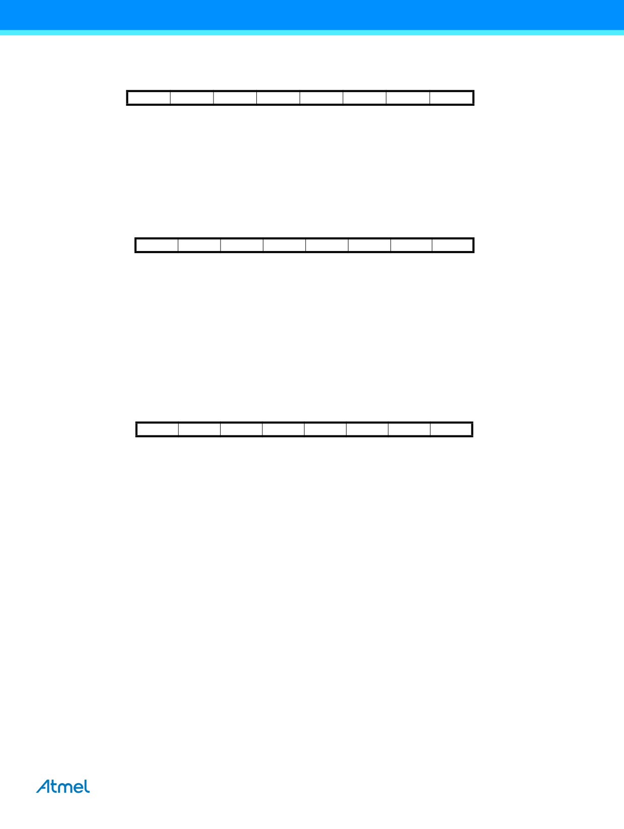
12.2.6
PCMSK2 - Pin Change Mask Register 2
Bit
7
6
5
4
3
2
1
0
(0x6D)
PCINT23
PCINT22
PCINT21
PCINT20
PCINT19
PCINT18
PCINT17
PCINT16
PCMSK2
Read/Write
R/W
R/W
R/W
R/W
R/W
R/W
R/W
R/W
Initial Value
0
0
0
0
0
0
0
0
• Bit 7..0 - PCINT23..16: Pin Change Enable Mask 23..16
Each PCINT23..16-bit selects whether pin change interrupt is enabled on the corresponding I/O pin. If PCINT23..16 is set
and the PCIE2 bit in PCICR is set, pin change interrupt is enabled on the corresponding I/O pin. If PCINT23..16 is cleared,
pin change interrupt on the corresponding I/O pin is disabled.
12.2.7
PCMSK1 - Pin Change Mask Register 1
Bit
7
6
5
4
3
2
1
0
(0x6C)
-
PCINT14
PCINT13
PCINT12
PCINT11
PCINT10
PCINT9
PCINT8
PCMSK1
Read/Write
R
R/W
R/W
R/W
R/W
R/W
R/W
R/W
Initial Value
0
0
0
0
0
0
0
0
• Bit 7 - Res: Reserved Bit
This bit is an unused bit in the Atmel® ATmega328P, and will always read as zero.
• Bit 6..0 - PCINT14..8: Pin Change Enable Mask 14..8
Each PCINT14..8-bit selects whether pin change interrupt is enabled on the corresponding I/O pin. If PCINT14..8 is set and
the PCIE1 bit in PCICR is set, pin change interrupt is enabled on the corresponding I/O pin. If PCINT14..8 is cleared, pin
change interrupt on the corresponding I/O pin is disabled.
12.2.8
PCMSK0 - Pin Change Mask Register 0
Bit
7
6
5
4
3
2
1
0
(0x6B)
PCINT7
PCINT6
PCINT5
PCINT4
PCINT3
PCINT2
PCINT1
PCINT0
PCMSK0
Read/Write
R/W
R/W
R/W
R/W
R/W
R/W
R/W
R/W
Initial Value
0
0
0
0
0
0
0
0
• Bit 7..0 - PCINT7..0: Pin Change Enable Mask 7..0
Each PCINT7..0 bit selects whether pin change interrupt is enabled on the corresponding I/O pin. If PCINT7..0 is set and the
PCIE0 bit in PCICR is set, pin change interrupt is enabled on the corresponding I/O pin. If PCINT7..0 is cleared, pin change
interrupt on the corresponding I/O pin is disabled.
ATmega328P [DATASHEET]
57
7810D-AVR-01/15
13.
I/O-Ports
13.1
Overview
All AVR® ports have true read-modify-write functionality when used as general digital I/O ports. This means that the direction
of one port pin can be changed without unintentionally changing the direction of any other pin with the SBI and CBI
instructions. The same applies when changing drive value (if configured as output) or enabling/disabling of pull-up resistors
(if configured as input). Each output buffer has symmetrical drive characteristics with both high sink and source capability.
The pin driver is strong enough to drive LED displays directly. All port pins have individually selectable pull-up resistors with
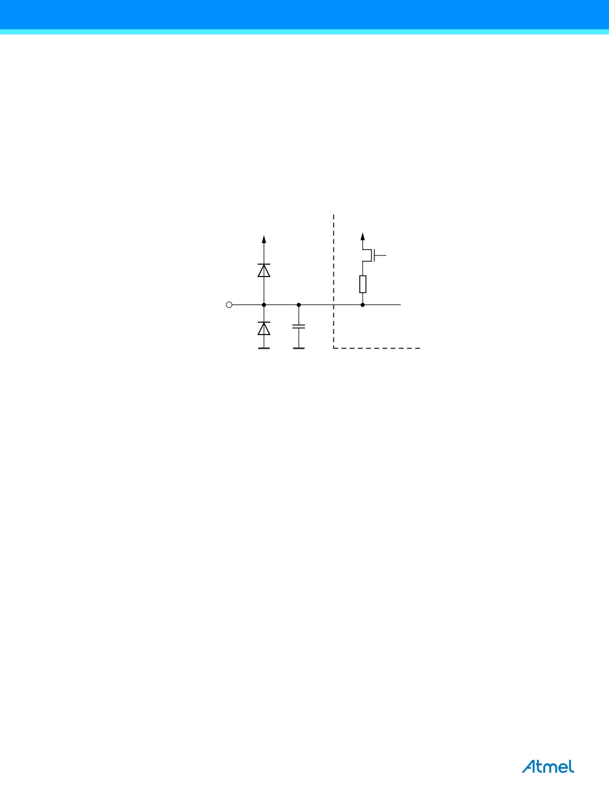
a supply-voltage invariant resistance. All I/O pins have protection diodes to both VCC and Ground as indicated in
Figure 13-1. Refer to Section 28. “Electrical Characteristics” on page 258 for a complete list of parameters.
Figure 13-1. I/O Pin Equivalent Schematic
Rpu
Pxn
Logic
See Figure
Cpin
”General Digital I/O”
for Details
All registers and bit references in this section are written in general form. A lower case “x” represents the numbering letter for
the port, and a lower case “n” represents the bit number. However, when using the register or bit defines in a program, the
precise form must be used. For example, PORTB3 for bit no. 3 in port B, here documented generally as PORTxn. The
physical I/O registers and bit locations are listed in Section 13.4 “Register Description” on page 72.
Three I/O memory address locations are allocated for each port, one each for the data register - PORTx, data direction
register - DDRx, and the port input pins - PINx. The port input pins I/O location is read only, while the data register and the
data direction register are read/write. However, writing a logic one to a bit in the PINx register, will result in a toggle in the
corresponding bit in the data register. In addition, the pull-up disable - PUD bit in MCUCR disables the pull-up function for all
pins in all ports when set.
Using the I/O port as general digital I/O is described in Section 13.2 “Ports as General Digital I/O” on page 59. Most port pins
are multiplexed with alternate functions for the peripheral features on the device. How each alternate function interferes with
the port pin is described in Section 13.3 “Alternate Port Functions” on page 63. Refer to the individual module sections for a
full description of the alternate functions. Note that enabling the alternate function of some of the port pins does not affect the
use of the other pins in the port as general digital I/O.
58
ATmega328P [DATASHEET]
7810D-AVR-01/15
13.2
Ports as General Digital I/O
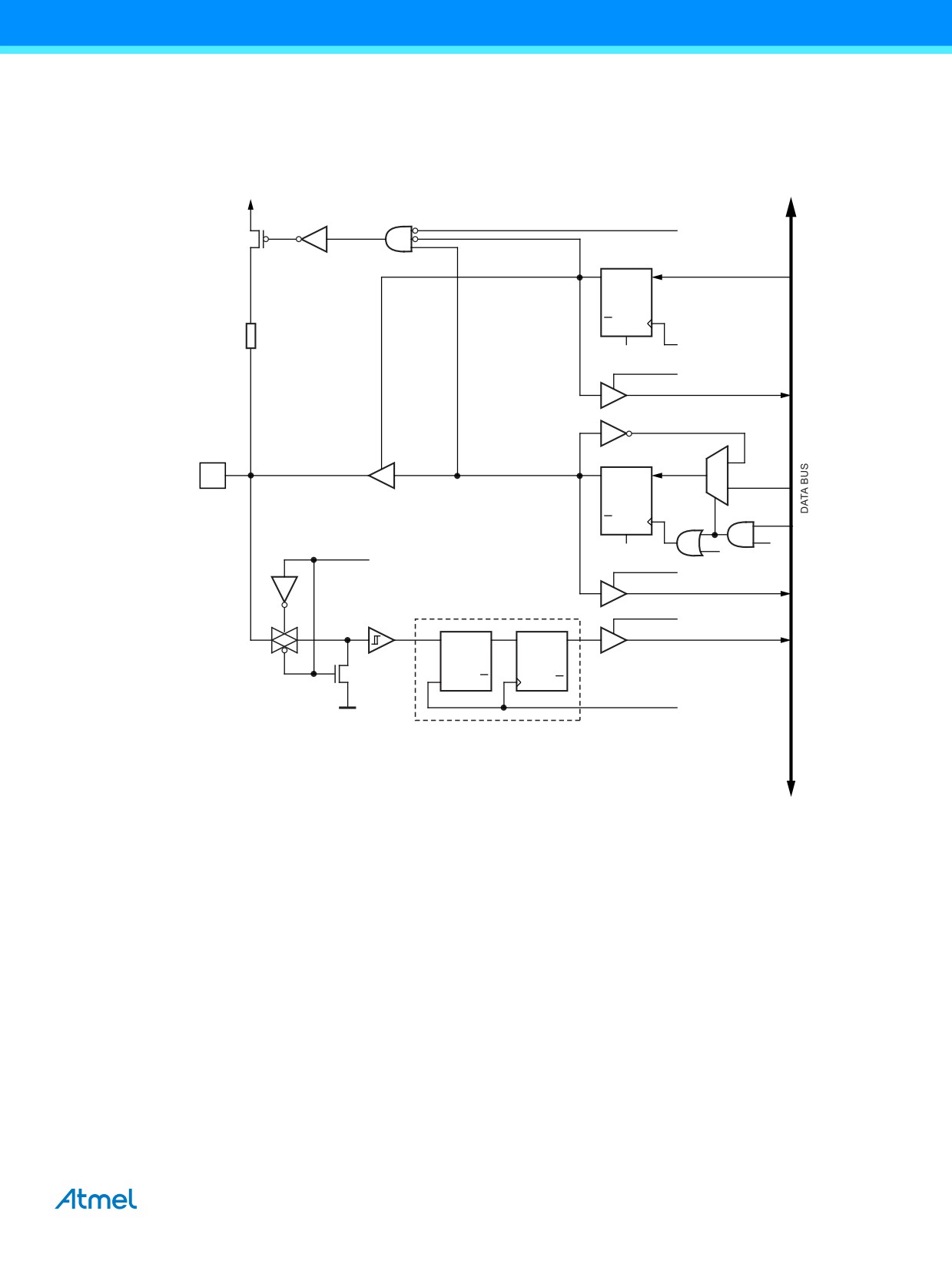
The ports are bi-directional I/O ports with optional internal pull-ups. Figure 13-2 shows a functional description of one
I/O-port pin, here generically called Pxn.
Figure 13-2. General Digital I/O(1)
PUD
Q
D
DDxn
Q
CLR
WDx
RESET
RDx
1
Pxn
Q
D
0
PORTxn
Q
CLR
RESET
WPx
SLEEP
WRx
RRx
Synchronizer
RPx
D
Q
D
Q
PINxn
L
Q
Q
CLKI/O
PUD:
PULLUP DISABLE
WDx:
WRITE DDRx
SLEEP:
SLEEP CONTROL
RDx:
READ DDRx
CLKI/O:
I/O CLOCK
WRx:
WRITE PORTx
RRx:
READ PORTx REGISTER
RPx:
READ PORTx PIN
WPx:
WRITE PINx REGISTER
Note:
1.
WRx, WPx, WDx, RRx, RPx, and RDx are common to all pins within the same port. clkI/O, SLEEP, and PUD
are common to all ports.
13.2.1
Configuring the Pin
Each port pin consists of three register bits: DDxn, PORTxn, and PINxn. As shown in Section 13.4 “Register Description” on
page 72, the DDxn bits are accessed at the DDRx I/O address, the PORTxn bits at the PORTx I/O address, and the PINxn
bits at the PINx I/O address.
The DDxn bit in the DDRx register selects the direction of this pin. If DDxn is written logic one, Pxn is configured as an output
pin. If DDxn is written logic zero, Pxn is configured as an input pin.
If PORTxn is written logic one when the pin is configured as an input pin, the pull-up resistor is activated. To switch the
pull-up resistor off, PORTxn has to be written logic zero or the pin has to be configured as an output pin. The port pins are
tri-stated when reset condition becomes active, even if no clocks are running.
If PORTxn is written logic one when the pin is configured as an output pin, the port pin is driven high (one). If PORTxn is
written logic zero when the pin is configured as an output pin, the port pin is driven low (zero).
ATmega328P [DATASHEET]
59
7810D-AVR-01/15
13.2.2
Toggling the Pin
Writing a logic one to PINxn toggles the value of PORTxn, independent on the value of DDRxn. Note that the SBI instruction
can be used to toggle one single bit in a port.
13.2.3
Switching Between Input and Output
When switching between tri-state ({DDxn, PORTxn} = 0b00) and output high ({DDxn, PORTxn} = 0b11), an intermediate
state with either pull-up enabled {DDxn, PORTxn} = 0b01) or output low ({DDxn, PORTxn} = 0b10) must occur. Normally, the
pull-up enabled state is fully acceptable, as a high-impedance environment will not notice the difference between a strong
high driver and a pull-up. If this is not the case, the PUD bit in the MCUCR register can be set to disable all pull-ups in all
ports.
Switching between input with pull-up and output low generates the same problem. The user must use either the tri-state
({DDxn, PORTxn} = 0b00) or the output high state ({DDxn, PORTxn} = 0b11) as an intermediate step.
Table 13-1 summarizes the control signals for the pin value.
Table 13-1. Port Pin Configurations
DDxn
PORTxn
PUD (in MCUCR)
I/O
Pull-up
Comment
0
0
X
Input
No
Tri-state (Hi-Z)
0
1
0
Input
Yes
Pxn will source current if ext. pulled low.
0
1
1
Input
No
Tri-state (Hi-Z)
1
0
X
Output
No
Output low (sink)
1
1
X
Output
No
Output high (source)
13.2.4
Reading the Pin Value
Independent of the setting of data direction bit DDxn, the port pin can be read through the PINxn register bit. As shown in
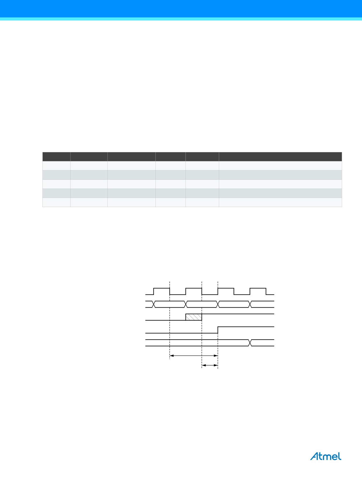
Figure 13-2, the PINxn register bit and the preceding latch constitute a synchronizer. This is needed to avoid metastability if
the physical pin changes value near the edge of the internal clock, but it also introduces a delay. Figure 13-3 shows a timing
diagram of the synchronization when reading an externally applied pin value. The maximum and minimum propagation
delays are denoted tpd,max and tpd,min respectively.
Figure 13-3. Synchronization when Reading an Externally Applied Pin Value
SYSTEM CLK
INSTRUCTIONS
XXX
XXX
in r17, PINx
SYNC LATCH
PINxn
r17
0x00
0xFF
tpd, max
tpd, min
Consider the clock period starting shortly after the first falling edge of the system clock. The latch is closed when the clock is
low, and goes transparent when the clock is high, as indicated by the shaded region of the “SYNC LATCH” signal. The signal
value is latched when the system clock goes low. It is clocked into the PINxn register at the succeeding positive clock edge.
As indicated by the two arrows tpd,max and tpd,min, a single signal transition on the pin will be delayed between ½ and 1½
system clock period depending upon the time of assertion.
When reading back a software assigned pin value, a nop instruction must be inserted as indicated in Figure 13-4 on page 61.
The out instruction sets the “SYNC LATCH” signal at the positive edge of the clock. In this case, the delay tpd through the
synchronizer is 1 system clock period.
60
ATmega328P [DATASHEET]
7810D-AVR-01/15
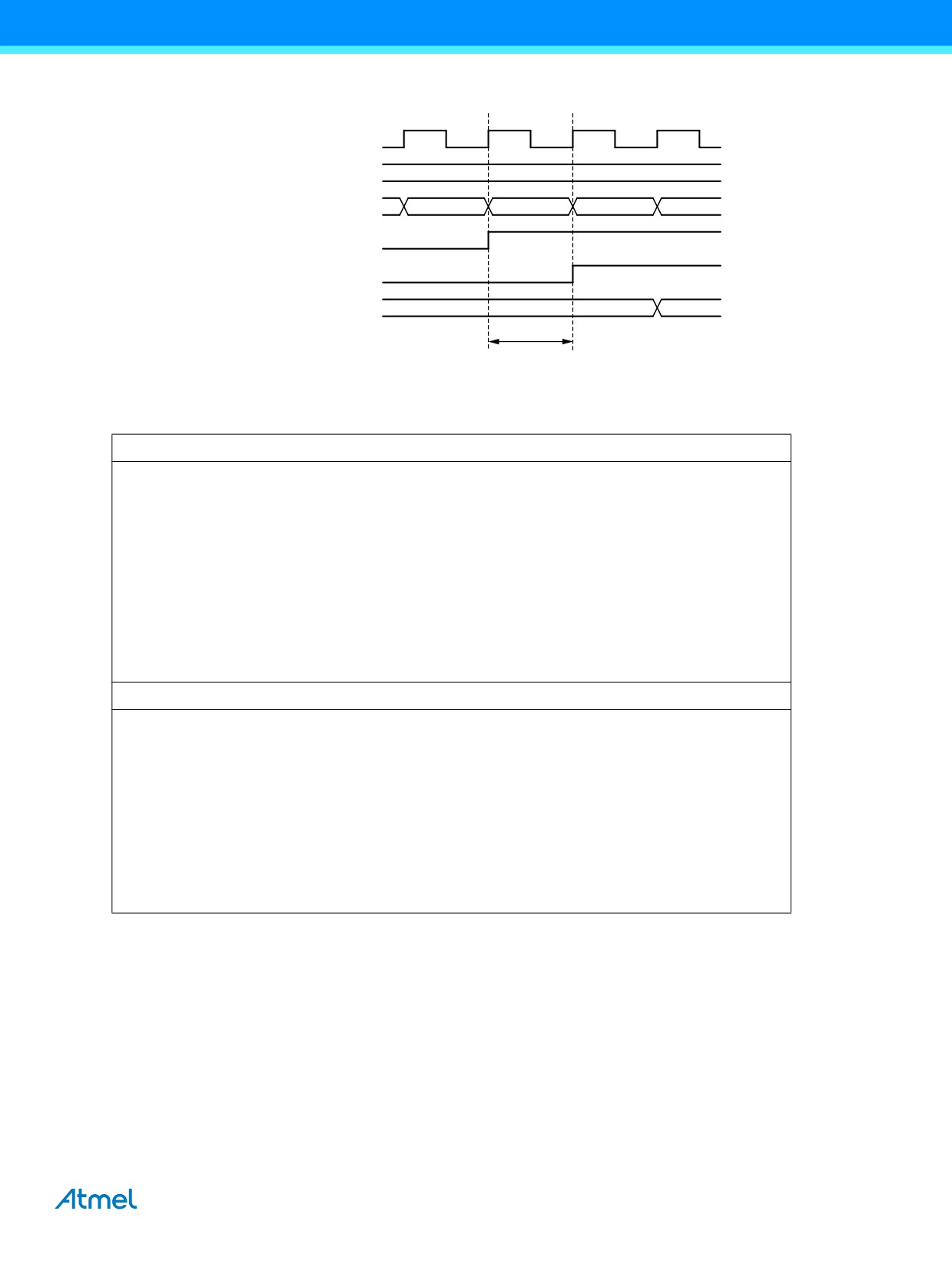
Figure 13-4. Synchronization when Reading a Software Assigned Pin Value
SYSTEM CLK
r16
0xFF
INSTRUCTIONS
out PORTx, r16
nop
in r17, PINx
SYNC LATCH
PINxn
r17
0x00
0xFF
tpd
The following code example shows how to set port B pins 0 and 1 high, 2 and 3 low, and define the port pins from 4 to 7 as
input with pull-ups assigned to port pins 6 and 7. The resulting pin values are read back again, but as previously discussed,
a nop instruction is included to be able to read back the value recently assigned to some of the pins.
Assembly Code Example(1)
; Define pull-ups and set outputs high
; Define directions for port pins
ldi
r16,(1<<PB7)|(1<<PB6)|(1<<PB1)|(1<<PB0)
ldi
r17,(1<<DDB3)|(1<<DDB2)|(1<<DDB1)|(1<<DDB0)
out
PORTB,r16
out
DDRB,r17
; Insert nop for synchronization
nop
; Read port pins
in
r16,PINB
C Code Example
unsigned char i;
/* Define pull-ups and set outputs high */
/* Define directions for port pins */
PORTB = (1<<PB7)|(1<<PB6)|(1<<PB1)|(1<<PB0);
DDRB = (1<<DDB3)|(1<<DDB2)|(1<<DDB1)|(1<<DDB0);
/* Insert nop for synchronization*/
__no_operation();
/* Read port pins */
i = PINB;
Note:
1.
For the assembly program, two temporary registers are used to minimize the time from pull-ups are set on pins
0, 1, 6, and 7, until the direction bits are correctly set, defining bit 2 and 3 as low and redefining bits 0 and 1 as
strong high drivers.
ATmega328P [DATASHEET]
61
7810D-AVR-01/15
13.2.5
Digital Input Enable and Sleep Modes
As shown in Figure 13-2, the digital input signal can be clamped to ground at the input of the Schmitt trigger. The signal
denoted SLEEP in the figure, is set by the MCU sleep controller in power-down mode, power-save mode, and standby mode
to avoid high power consumption if some input signals are left floating, or have an analog signal level close to VCC/2.
SLEEP is overridden for port pins enabled as external interrupt pins. If the external interrupt request is not enabled, SLEEP
is active also for these pins. SLEEP is also overridden by various other alternate functions as described in Section 13.3
“Alternate Port Functions” on page 63.
If a logic high level (“one”) is present on an asynchronous external interrupt pin configured as “interrupt on rising edge, falling
edge, or any logic change on pin” while the external interrupt is not enabled, the corresponding external interrupt flag will be
set when resuming from the above mentioned sleep mode, as the clamping in these sleep mode produces the requested
logic change.
13.2.6
Unconnected Pins
If some pins are unused, it is recommended to ensure that these pins have a defined level. Even though most of the digital
inputs are disabled in the deep sleep modes as described above, floating inputs should be avoided to reduce current
consumption in all other modes where the digital inputs are enabled (reset, active mode and idle mode).
The simplest method to ensure a defined level of an unused pin, is to enable the internal pull-up. In this case, the pull-up will
be disabled during reset. If low power consumption during reset is important, it is recommended to use an external pull-up or
pull-down. Connecting unused pins directly to VCC or GND is not recommended, since this may cause excessive currents if
the pin is accidentally configured as an output.
62
ATmega328P [DATASHEET]
7810D-AVR-01/15
13.3
Alternate Port Functions
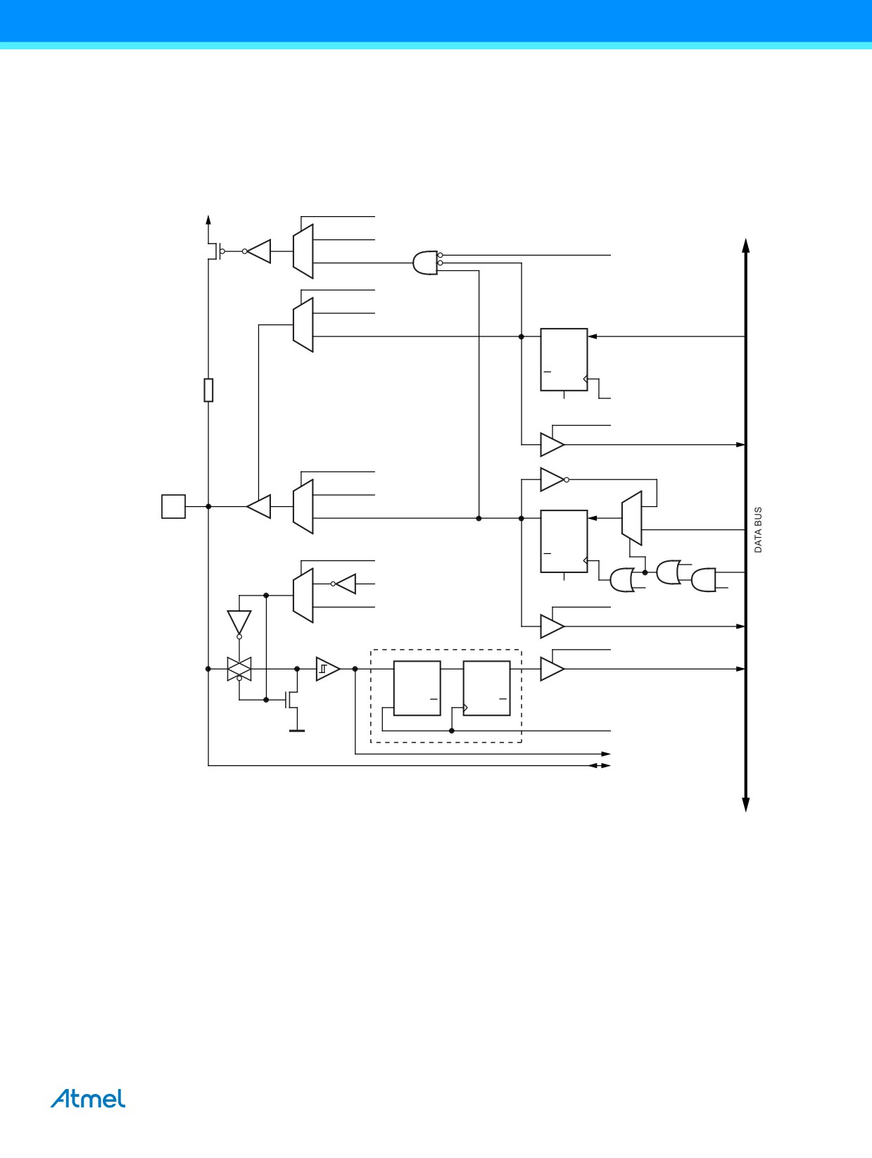
Most port pins have alternate functions in addition to being general digital I/Os. Figure 13-5 shows how the port pin control
signals from the simplified Figure 13-2 on page 59 can be overridden by alternate functions. The overriding signals may not
be present in all port pins, but the figure serves as a generic description applicable to all port pins in the AVR®
microcontroller family.
Figure 13-5. Alternate Port Functions(1)
PUOExn
1
PUOVxn
PUD
0
DDOExn
1
DDOVxn
0
Q
D
DDxn
Q
CLR
WDx
RESET
RDx
PVOExn
1
PVOVxn
Pxn
1
0
Q
D
0
PORTxn
DIEOExn
Q
PTOExn
CLR
1
DIEOVxn
RESET
WRx
WPx
0
RRx
SLEEP
Synchronizer
RPx
D SET Q
D
Q
PINxn
L
Q
Q
CLR
CLR
CLKI/O
DIxn
AIOxn
PUOExn:
Pxn PULL-UP OVERRIDE ENABLE
PUD:
PULL-UP DISABLE
PUOVxn:
Pxn PULL-UP OVERRIDE VALUE
WDx:
WRITE DDRx
DDOExn:
Pxn DATA DIRECTION OVERRIDE ENABLE
RDx:
READ DDRx
DDOVxn:
Pxn DATA DIRECTION OVERRIDE VALUE
RRx:
READ PORTx REGISTER
PVOExn:
Pxn PORT VALUE OVERRIDE ENABLE
WRx:
WRITE PORTx
PVOVxn:
Pxn PORT VALUE OVERRIDE VALUE
RPx:
READ PORTx PIN
DIEOExn:
Pxn DIGITAL INPUT ENABLE OVERRIDE ENABLE
WPx:
WRITE PINx
DIEOVxn:
Pxn DIGITAL INPUT ENABLE OVERRIDE VALUE
CLK:I/O
I/O CLOCK
SLEEP:
SLEEP CONTROL
DIxn:
DIGITAL INPUT PIN n ON PORTx
PTOExn:
Pxn, PORT TOGGLE OVERRIDE ENABLE
AIOxn:
ANALOG INPUT/OUTPUT PIN n ON PORTx
Note:
1.
WRx, WPx, WDx, RRx, RPx, and RDx are common to all pins within the same port. clkI/O, SLEEP, and PUD
are common to all ports. All other signals are unique for each pin.
ATmega328P [DATASHEET]
63
7810D-AVR-01/15

Table 13-2 summarizes the function of the overriding signals. The pin and port indexes from Figure 13-5 on page 63 are not
shown in the succeeding tables. The overriding signals are generated internally in the modules having the alternate function.
Table 13-2. Generic Description of Overriding Signals for Alternate Functions
Signal Name
Full Name
Description
If this signal is set, the pull-up enable is controlled by the PUOV signal. If
PUOE
Pull-up override enable
this signal is cleared, the pull-up is enabled when {DDxn, PORTxn,
PUD} = 0b010.
If PUOE is set, the pull-up is enabled/disabled when PUOV is set/cleared,
PUOV
Pull-up override value
regardless of the setting of the DDxn, PORTxn, and PUD register bits.
If this signal is set, the output driver enable is controlled by the DDOV
Data direction override
DDOE
signal. If this signal is cleared, the output driver is enabled by the DDxn
enable
register bit.
Data direction override
If DDOE is set, the output driver is enabled/disabled when DDOV is
DDOV
value
set/cleared, regardless of the setting of the DDxn register bit.
If this signal is set and the output driver is enabled, the port value is
Port value override
PVOE
controlled by the PVOV signal. If PVOE is cleared, and the output driver is
enable
enabled, the port value is controlled by the PORTxn register bit.
If PVOE is set, the port value is set to PVOV, regardless of the setting of the
PVOV
Port value override value
PORTxn register bit.
Port toggle override
PTOE
If PTOE is set, the PORTxn register bit is inverted.
enable
If this bit is set, the digital input enable is controlled by the DIEOV signal. If
Digital input enable
DIEOE
this signal is cleared, the digital input enable is determined by MCU state
override enable
(normal mode, sleep mode).
Digital input enable
If DIEOE is set, the digital input is enabled/disabled when DIEOV is
DIEOV
override value
set/cleared, regardless of the MCU state (normal mode, sleep mode).
This is the digital input to alternate functions. In the figure, the signal is
connected to the output of the schmitt trigger but before the synchronizer.
DI
Digital input
Unless the digital input is used as a clock source, the module with the
alternate function will use its own synchronizer.
This is the analog input/output to/from alternate functions. The signal is
AIO
Analog input/output
connected directly to the pad, and can be used bi-directionally.
The following subsections shortly describe the alternate functions for each port, and relate the overriding signals to the
alternate function. Refer to the alternate function description for further details.
64
ATmega328P [DATASHEET]
7810D-AVR-01/15

13.3.1
Alternate Functions of Port B
The port B pins with alternate functions are shown in Table 13-3.
Table 13-3. Port B Pins Alternate Functions
Port Pin
Alternate Functions
XTAL2 (chip clock oscillator pin 2)
PB7
TOSC2 (timer oscillator pin 2)
PCINT7 (pin change interrupt 7)
XTAL1 (chip clock oscillator pin 1 or external clock input)
PB6
TOSC1 (timer oscillator pin 1)
PCINT6 (pin change interrupt 6)
SCK (SPI bus master clock input)
PB5
PCINT5 (pin change interrupt 5)
MISO (SPI bus master input/slave output)
PB4
PCINT4 (pin change interrupt 4)
MOSI (SPI bus master output/slave input)
PB3
OC2A (Timer/Counter2 output compare match A output)
PCINT3 (pin change interrupt 3)
SS (SPI bus master slave select)
PB2
OC1B (Timer/Counter1 output compare match B output)
PCINT2 (pin change interrupt 2)
OC1A (Timer/Counter1 output compare match A output)
PB1
PCINT1 (pin change interrupt 1)
ICP1 (Timer/Counter1 input capture input)
PB0
CLKO (divided system clock output)
PCINT0 (pin change interrupt 0)
The alternate pin configuration is as follows:
• XTAL2/TOSC2/PCINT7 - Port B, Bit 7
XTAL2: Chip clock oscillator pin 2. Used as clock pin for crystal oscillator or low-frequency crystal oscillator. When used as a
clock pin, the pin can not be used as an I/O pin.
TOSC2: Timer oscillator pin 2. Used only if internal calibrated RC oscillator is selected as chip clock source, and the
asynchronous timer is enabled by the correct setting in ASSR. When the AS2 bit in ASSR is set (one) and the EXCLK bit is
cleared (zero) to enable asynchronous clocking of Timer/Counter2 using the crystal oscillator, pin PB7 is disconnected from
the port, and becomes the inverting output of the oscillator amplifier. In this mode, a crystal oscillator is connected to this pin,
and the pin cannot be used as an I/O pin.
PCINT7: Pin change interrupt source 7. The PB7 pin can serve as an external interrupt source.
If PB7 is used as a clock pin, DDB7, PORTB7 and PINB7 will all read 0.
• XTAL1/TOSC1/PCINT6 - Port B, Bit 6
XTAL1: Chip clock oscillator pin 1. Used for all chip clock sources except internal calibrated RC oscillator. When used as a
clock pin, the pin can not be used as an I/O pin.
TOSC1: Timer oscillator pin 1. Used only if internal calibrated RC oscillator is selected as chip clock source, and the
asynchronous timer is enabled by the correct setting in ASSR. When the AS2 bit in ASSR is set (one) to enable
asynchronous clocking of Timer/Counter2, pin PB6 is disconnected from the port, and becomes the input of the inverting
oscillator amplifier. In this mode, a crystal oscillator is connected to this pin, and the pin can not be used as an I/O pin.
PCINT6: Pin change interrupt source 6. The PB6 pin can serve as an external interrupt source.
If PB6 is used as a clock pin, DDB6, PORTB6 and PINB6 will all read 0.
ATmega328P [DATASHEET]
65
7810D-AVR-01/15
• SCK/PCINT5 - Port B, Bit 5
SCK: Master clock output, slave clock input pin for SPI channel. When the SPI is enabled as a slave, this pin is configured as
an input regardless of the setting of DDB5. When the SPI is enabled as a master, the data direction of this pin is controlled
by DDB5. When the pin is forced by the SPI to be an input, the pull-up can still be controlled by the PORTB5 bit.
PCINT5: Pin change interrupt source 5. The PB5 pin can serve as an external interrupt source.
• MISO/PCINT4 - Port B, Bit 4
MISO: Master data input, slave data output pin for SPI channel. When the SPI is enabled as a master, this pin is configured
as an input regardless of the setting of DDB4. When the SPI is enabled as a slave, the data direction of this pin is controlled
by DDB4. When the pin is forced by the SPI to be an input, the pull-up can still be controlled by the PORTB4 bit.
PCINT4: Pin change interrupt source 4. The PB4 pin can serve as an external interrupt source.
• MOSI/OC2/PCINT3 - Port B, Bit 3
MOSI: SPI master data output, slave data input for SPI channel. When the SPI is enabled as a slave, this pin is configured
as an input regardless of the setting of DDB3. When the SPI is enabled as a master, the data direction of this pin is
controlled by DDB3. When the pin is forced by the SPI to be an input, the pull-up can still be controlled by the PORTB3 bit.
OC2, output compare match output: The PB3 pin can serve as an external output for the Timer/Counter2 compare match.
The PB3 pin has to be configured as an output (DDB3 set (one)) to serve this function. The OC2 pin is also the output pin for
the PWM mode timer function.
PCINT3: Pin change interrupt source 3. The PB3 pin can serve as an external interrupt source.
• SS/OC1B/PCINT2 - Port B, Bit 2
SS: Slave select input. When the SPI is enabled as a slave, this pin is configured as an input regardless of the setting of
DDB2. As a slave, the SPI is activated when this pin is driven low. When the SPI is enabled as a master, the data direction
of this pin is controlled by DDB2. When the pin is forced by the SPI to be an input, the pull-up can still be controlled by the
PORTB2 bit.
OC1B, output compare match output: The PB2 pin can serve as an external output for the Timer/Counter1 compare match
B. The PB2 pin has to be configured as an output (DDB2 set (one)) to serve this function. The OC1B pin is also the output
pin for the PWM mode timer function.
PCINT2: Pin change interrupt source 2. The PB2 pin can serve as an external interrupt source.
• OC1A/PCINT1 - Port B, Bit 1
OC1A, output compare match output: The PB1 pin can serve as an external output for the Timer/Counter1 compare match
A. The PB1 pin has to be configured as an output (DDB1 set (one)) to serve this function. The OC1A pin is also the output
pin for the PWM mode timer function.
PCINT1: Pin change interrupt source 1. The PB1 pin can serve as an external interrupt source.
• ICP1/CLKO/PCINT0 - Port B, Bit 0
ICP1, input capture pin: The PB0 pin can act as an input capture pin for Timer/Counter1.
CLKO, divided system clock: The divided system clock can be output on the PB0 pin. The divided system clock will be output
if the CKOUT fuse is programmed, regardless of the PORTB0 and DDB0 settings. It will also be output during reset.
PCINT0: Pin change interrupt source 0. The PB0 pin can serve as an external interrupt source.
Table 13-4 on page 67 and Table 13-5 on page 67 relate the alternate functions of Port B to the overriding signals shown in
Figure 13-5 on page 63. SPI MSTR INPUT and SPI SLAVE OUTPUT constitute the MISO signal, while MOSI is divided into
SPI MSTR OUTPUT and SPI SLAVE INPUT.
66
ATmega328P [DATASHEET]
7810D-AVR-01/15
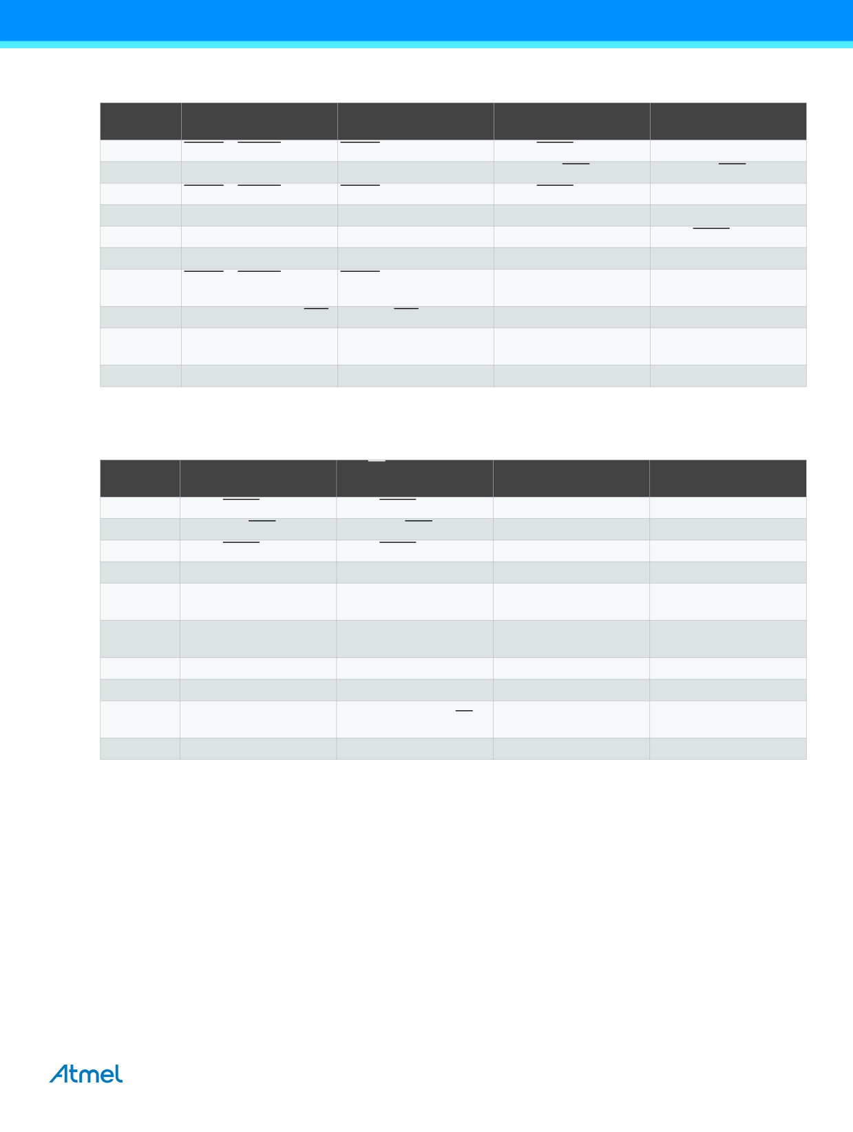
Table 13-4.
Overriding Signals for Alternate Functions in PB7..PB4
Signal
PB7/XTAL2/
PB6/XTAL1/
PB5/SCK/
PB4/MISO/
Name
TOSC2/PCINT7(1)
TOSC1/PCINT6(1)
PCINT5
PCINT4
PUOE
INTRC EXTCK + AS2
INTRC + AS2
SPE MSTR
SPE MSTR
PUOV
0
0
PORTB5 PUD
PORTB4 PUD
DDOE
INTRC EXTCK + AS2
INTRC + AS2
SPE MSTR
SPE MSTR
DDOV
0
0
0
0
PVOE
0
0
SPE MSTR
SPE MSTR
PVOV
0
0
SCK OUTPUT
SPI SLAVE OUTPUT
INTRC EXTCK + AS2 +
INTRC + AS2 + PCINT6
DIEOE
PCINT5 PCIE0
PCINT4 PCIE0
PCINT7 PCIE0
PCIE0
DIEOV
(INTRC + EXTCK) AS2
INTRC AS2
1
1
PCINT5 INPUT SCK
PCINT4 INPUT SPI
DI
PCINT7 INPUT
PCINT6 INPUT
INPUT
MSTR INPUT
AIO
Oscillator output
Oscillator/clock input
-
-
Note:
1.
INTRC means that one of the internal RC oscillators are selected (by the CKSEL fuses), EXTCK means that
external clock is selected (by the CKSEL fuses)
Table 13-5.
Overriding Signals for Alternate Functions in PB3..PB0
Signal
PB3/MOSI/
PB2/SS/
PB1/OC1A/
PB0/ICP1/
Name
OC2/PCINT3
OC1B/PCINT2
PCINT1
PCINT0
PUOE
SPE MSTR
SPE MSTR
0
0
PUOV
PORTB3 PUD
PORTB2 PUD
0
0
DDOE
SPE MSTR
SPE MSTR
0
0
DDOV
0
0
0
0
SPE MSTR +
PVOE
OC1B ENABLE
OC1A ENABLE
0
OC2A ENABLE
SPI MSTR OUTPUT +
PVOV
OC1B
OC1A
0
OC2A
DIEOE
PCINT3 PCIE0
PCINT2 PCIE0
PCINT1 PCIE0
PCINT0 PCIE0
DIEOV
1
1
1
1
PCINT3 INPUT SPI
PCINT0 INPUT ICP1
DI
PCINT2 INPUT SPI SS
PCINT1 INPUT
SLAVE INPUT
INPUT
AIO
-
-
-
-
ATmega328P [DATASHEET]
67
7810D-AVR-01/15

13.3.2
Alternate Functions of Port C
The port C pins with alternate functions are shown in Table 13-6.
Table 13-6. Port C Pins Alternate Functions
Port Pin
Alternate Function
RESET (reset pin)
PC6
PCINT14 (pin change interrupt 14)
ADC5 (ADC input channel 5)
PC5
SCL (2-wire serial bus clock line)
PCINT13 (pin change interrupt 13)
ADC4 (ADC input channel 4)
PC4
SDA (2-wire serial bus data input/output line)
PCINT12 (pin change interrupt 12)
ADC3 (ADC input channel 3)
PC3
PCINT11 (pin change interrupt 11)
ADC2 (ADC input channel 2)
PC2
PCINT10 (pin change interrupt 10)
ADC1 (ADC input channel 1)
PC1
PCINT9 (pin change interrupt 9)
ADC0 (ADC input channel 0)
PC0
PCINT8 (pin change interrupt 8)
The alternate pin configuration is as follows:
• RESET/PCINT14 - Port C, Bit 6
RESET, Reset pin: When the RSTDISBL fuse is programmed, this pin functions as an input pin, and the part will have to rely
on power-on reset and brown-out reset as its reset sources. When the RSTDISBL fuse is unprogrammed, the reset circuitry
is connected to the pin, and the pin can not be used as an input pin.
If PC6 is used as a reset pin, DDC6, PORTC6 and PINC6 will all read 0.
PCINT14: Pin change interrupt source 14. The PC6 pin can serve as an external interrupt source.
• SCL/ADC5/PCINT13 - Port C, Bit 5
SCL, 2-wire serial interface clock: When the TWEN bit in TWCR is set (one) to enable the 2-wire serial interface, pin PC5 is
disconnected from the port and becomes the serial clock I/O pin for the 2-wire serial interface. In this mode, there is a spike
filter on the pin to suppress spikes shorter than 50ns on the input signal, and the pin is driven by an open drain driver with
slew-rate limitation.
PC5 can also be used as ADC input channel 5. Note that ADC input channel 5 uses digital power.
PCINT13: Pin change interrupt source 13. The PC5 pin can serve as an external interrupt source.
• SDA/ADC4/PCINT12 - Port C, Bit 4
SDA, 2-wire serial interface data: When the TWEN bit in TWCR is set (one) to enable the 2-wire serial interface, pin PC4 is
disconnected from the port and becomes the serial data I/O pin for the 2-wire serial interface. In this mode, there is a spike
filter on the pin to suppress spikes shorter than 50ns on the input signal, and the pin is driven by an open drain driver with
slew-rate limitation.
PC4 can also be used as ADC input Channel 4. Note that ADC input channel 4 uses digital power.
PCINT12: Pin change interrupt source 12. The PC4 pin can serve as an external interrupt source.
• ADC3/PCINT11 - Port C, Bit 3
PC3 can also be used as ADC input Channel 3. Note that ADC input channel 3 uses analog power.
PCINT11: Pin change interrupt source 11. The PC3 pin can serve as an external interrupt source.
68
ATmega328P [DATASHEET]
7810D-AVR-01/15

• ADC2/PCINT10 - Port C, Bit 2
PC2 can also be used as ADC input channel 2. Note that ADC input channel 2 uses analog power.
PCINT10: Pin change interrupt source 10. The PC2 pin can serve as an external interrupt source.
• ADC1/PCINT9 - Port C, Bit 1
PC1 can also be used as ADC input channel 1. Note that ADC input channel 1 uses analog power.
PCINT9: Pin change interrupt source 9. The PC1 pin can serve as an external interrupt source.
• ADC0/PCINT8 - Port C, Bit 0
PC0 can also be used as ADC input channel 0. Note that ADC input channel 0 uses analog power.
PCINT8: Pin change interrupt source 8. The PC0 pin can serve as an external interrupt source.
Table 13-7 and Table 13-8 relate the alternate functions of port C to the overriding signals shown in Figure 13-5 on page 63.
Table 13-7. Overriding Signals for Alternate Functions in PC6..PC4(1)
Signal Name
PC6/RESET/PCINT14
PC5/SCL/ADC5/PCINT13
PC4/SDA/ADC4/PCINT12
PUOE
RSTDISBL
TWEN
TWEN
PUOV
1
PORTC5 PUD
PORTC4 PUD
DDOE
RSTDISBL
TWEN
TWEN
DDOV
0
SCL_OUT
SDA_OUT
PVOE
0
TWEN
TWEN
PVOV
0
0
0
DIEOE
RSTDISBL + PCINT14 PCIE1
PCINT13 PCIE1 + ADC5D
PCINT12 PCIE1 + ADC4D
DIEOV
RSTDISBL
PCINT13 PCIE1
PCINT12 PCIE1
DI
PCINT14 INPUT
PCINT13 INPUT
PCINT12 INPUT
AIO
RESET INPUT
ADC5 INPUT / SCL INPUT
ADC4 INPUT / SDA INPUT
Note:
1.
When enabled, the 2-wire serial interface enables slew-rate controls on the output pins PC4 and PC5. This is
not shown in the figure. In addition, spike filters are connected between the AIO outputs shown in the port
figure and the digital logic of the TWI module.
Table 13-8.
Overriding Signals for Alternate Functions in PC3..PC0
Signal
PC3/ADC3/
PC2/ADC2/
PC1/ADC1/
PC0/ADC0/
Name
PCINT11
PCINT10
PCINT9
PCINT8
PUOE
0
0
0
0
PUOV
0
0
0
0
DDOE
0
0
0
0
DDOV
0
0
0
0
PVOE
0
0
0
0
PVOV
0
0
0
0
PCINT11 PCIE1 +
PCINT10 PCIE1 +
PCINT9 PCIE1 +
PCINT8 PCIE1 +
DIEOE
ADC3D
ADC2D
ADC1D
ADC0D
DIEOV
PCINT11 PCIE1
PCINT10 PCIE1
PCINT9 PCIE1
PCINT8 PCIE1
DI
PCINT11 INPUT
PCINT10 INPUT
PCINT9 INPUT
PCINT8 INPUT
AIO
ADC3 INPUT
ADC2 INPUT
ADC1 INPUT
ADC0 INPUT
ATmega328P [DATASHEET]
69
7810D-AVR-01/15

13.3.3
Alternate Functions of Port D
The port D pins with alternate functions are shown in Table 13-9.
Table 13-9. Port D Pins Alternate Functions
Port Pin
Alternate Function
AIN1 (analog comparator negative input)
PD7
PCINT23 (Pin Change Interrupt 23)
AIN0 (analog comparator positive input)
PD6
OC0A (Timer/Counter0 output compare match A output)
PCINT22 (pin change interrupt 22)
T1 (Timer/Counter 1 external counter input)
PD5
OC0B (Timer/Counter0 output compare match B output)
PCINT21 (pin change interrupt 21)
XCK (USART external clock input/output)
PD4
T0 (Timer/Counter 0 external counter input)
PCINT20 (pin change interrupt 20)
INT1 (external interrupt 1 input)
PD3
OC2B (Timer/Counter2 output compare match B output)
PCINT19 (pin change interrupt 19)
INT0 (external interrupt 0 input)
PD2
PCINT18 (pin change interrupt 18)
TXD (USART output pin)
PD1
PCINT17 (pin change interrupt 17)
RXD (USART input pin)
PD0
PCINT16 (pin change interrupt 16)
The alternate pin configuration is as follows:
• AIN1/OC2B/PCINT23 - Port D, Bit 7
AIN1, analog comparator negative input. Configure the port pin as input with the internal pull-up switched off to avoid the
digital port function from interfering with the function of the analog comparator.
PCINT23: Pin change interrupt source 23. The PD7 pin can serve as an external interrupt source.
• AIN0/OC0A/PCINT22 - Port D, Bit 6
AIN0, analog comparator positive input. Configure the port pin as input with the internal pull-up switched off to avoid the
digital port function from interfering with the function of the analog comparator.
OC0A, output compare match output: The PD6 pin can serve as an external output for the Timer/Counter0 compare match
A. The PD6 pin has to be configured as an output (DDD6 set (one)) to serve this function. The OC0A pin is also the output
pin for the PWM mode timer function.
PCINT22: Pin change interrupt source 22. The PD6 pin can serve as an external interrupt source.
• T1/OC0B/PCINT21 - Port D, Bit 5
T1, Timer/Counter1 counter source.
OC0B, output compare match output: The PD5 pin can serve as an external output for the Timer/Counter0 compare match
B. The PD5 pin has to be configured as an output (DDD5 set (one)) to serve this function. The OC0B pin is also the output
pin for the PWM mode timer function.
PCINT21: Pin change interrupt source 21. The PD5 pin can serve as an external interrupt source.
• XCK/T0/PCINT20 - Port D, Bit 4
XCK, USART external clock.
T0, Timer/Counter0 counter source.
PCINT20: Pin change interrupt source 20. The PD4 pin can serve as an external interrupt source.
70
ATmega328P [DATASHEET]
7810D-AVR-01/15

• INT1/OC2B/PCINT19 - Port D, Bit 3
INT1, external interrupt source 1: The PD3 pin can serve as an external interrupt source.
OC2B, output compare match output: The PD3 pin can serve as an external output for the Timer/Counter0 compare match
B. The PD3 pin has to be configured as an output (DDD3 set (one)) to serve this function. The OC2B pin is also the output
pin for the PWM mode timer function.
PCINT19: Pin change interrupt source 19. The PD3 pin can serve as an external interrupt source.
• INT0/PCINT18 - Port D, Bit 2
INT0, external interrupt source 0: The PD2 pin can serve as an external interrupt source.
PCINT18: Pin change interrupt source 18. The PD2 pin can serve as an external interrupt source.
• TXD/PCINT17 - Port D, Bit 1
TXD, transmit Data (data output pin for the USART). When the USART transmitter is enabled, this pin is configured as an
output regardless of the value of DDD1.
PCINT17: Pin change interrupt source 17. The PD1 pin can serve as an external interrupt source.
• RXD/PCINT16 - Port D, Bit 0
RXD, Receive Data (data input pin for the USART). When the USART receiver is enabled this pin is configured as an input
regardless of the value of DDD0. When the USART forces this pin to be an input, the pull-up can still be controlled by the
PORTD0 bit.
PCINT16: Pin change interrupt source 16. The PD0 pin can serve as an external interrupt source.
Table 13-10 and Table 13-11 on page 72 relate the alternate functions of port D to the overriding signals shown in
Figure 13-5 on page 63.
Table 13-10. Overriding Signals for Alternate Functions PD7..PD4
Signal Name
PD7/AIN1/PCINT23
PD6/AIN0/OC0A/PCINT22
PD5/T1/OC0B/PCINT21
PD4/XCK/T0/PCINT20
PUOE
0
0
0
0
PUO
0
0
0
0
DDOE
0
0
0
0
DDOV
0
0
0
0
PVOE
0
OC0A ENABLE
OC0B ENABLE
UMSEL
PVOV
0
OC0A
OC0B
XCK OUTPUT
DIEOE
PCINT23 PCIE2
PCINT22 PCIE2
PCINT21 PCIE2
PCINT20 PCIE2
DIEOV
1
1
1
1
PCINT21 INPUT
PCINT20 INPUT XCK
DI
PCINT23 INPUT
PCINT22 INPUT
T1 INPUT
INPUT T0 INPUT
AIO
AIN1 INPUT
AIN0 INPUT
-
-
ATmega328P [DATASHEET]
71
7810D-AVR-01/15
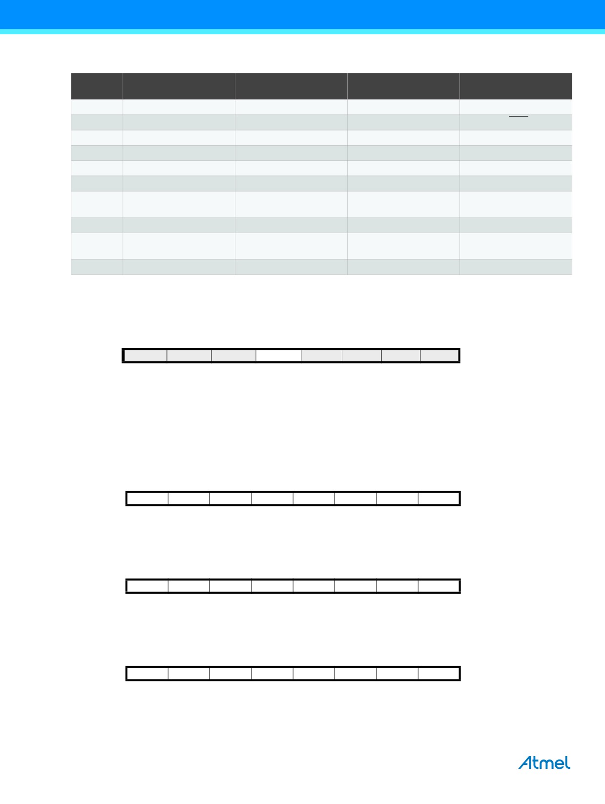
Table 13-11. Overriding Signals for Alternate Functions in PD3..PD0
Signal
PD3/OC2B/INT1/
PD2/INT0/
PD1/TXD/
PD0/RXD/
Name
PCINT19
PCINT18
PCINT17
PCINT16
PUOE
0
0
TXEN
RXEN
PUO
0
0
0
PORTD0 PUD
DDOE
0
0
TXEN
RXEN
DDOV
0
0
1
0
PVOE
OC2B ENABLE
0
TXEN
0
PVOV
OC2B
0
TXD
0
INT1 ENABLE + PCINT19
INT0 ENABLE + PCINT18
DIEOE
PCINT17 PCIE2
PCINT16 PCIE2
PCIE2
PCIE1
DIEOV
1
1
1
1
PCINT19 INPUT
PCINT18 INPUT
PCINT16 INPUT
DI
PCINT17 INPUT
INT1 INPUT
INT0 INPUT
RXD
AIO
-
-
-
-
13.4
Register Description
13.4.1
MCUCR - MCU Control Register
Bit
7
6
5
4
3
2
1
0
0x35 (0x55)
-
BODS
BODSE
PUD
-
-
IVSEL
IVCE
MCUCR
Read/Write
R
R
R
R/W
R
R
R/W
R/W
Initial Value
0
0
0
0
0
0
0
0
• Bit 4 - PUD: Pull-up Disable
When this bit is written to one, the pull-ups in the I/O ports are disabled even if the DDxn and PORTxn registers are
configured to enable the pull-ups ({DDxn, PORTxn} = 0b01). See Section 13.2.1 “Configuring the Pin” on page 59 for more
details about this feature.
13.4.2
PORTB - The Port B Data Register
Bit
7
6
5
4
3
2
1
0
0x05 (0x25)
PORTB7
PORTB6
PORTB5
PORTB4
PORTB3
PORTB2
PORTB1
PORTB0
PORTB
Read/Write
R/W
R/W
R/W
R/W
R/W
R/W
R/W
R/W
Initial Value
0
0
0
0
0
0
0
0
13.4.3
DDRB - The Port B Data Direction Register
Bit
7
6
5
4
3
2
1
0
0x04 (0x24)
DDB7
DDB6
DDB5
DDB4
DDB3
DDB2
DDB1
DDB0
DDRB
Read/Write
R/W
R/W
R/W
R/W
R/W
R/W
R/W
R/W
Initial Value
0
0
0
0
0
0
0
0
13.4.4
PINB - The Port B Input Pins Address
Bit
7
6
5
4
3
2
1
0
0x03 (0x23)
PINB7
PINB6
PINB5
PINB4
PINB3
PINB2
PINB1
PINB0
PINB
Read/Write
R
R
R
R
R
R
R
R
Initial Value
N/A
N/A
N/A
N/A
N/A
N/A
N/A
N/A
72
ATmega328P [DATASHEET]
7810D-AVR-01/15
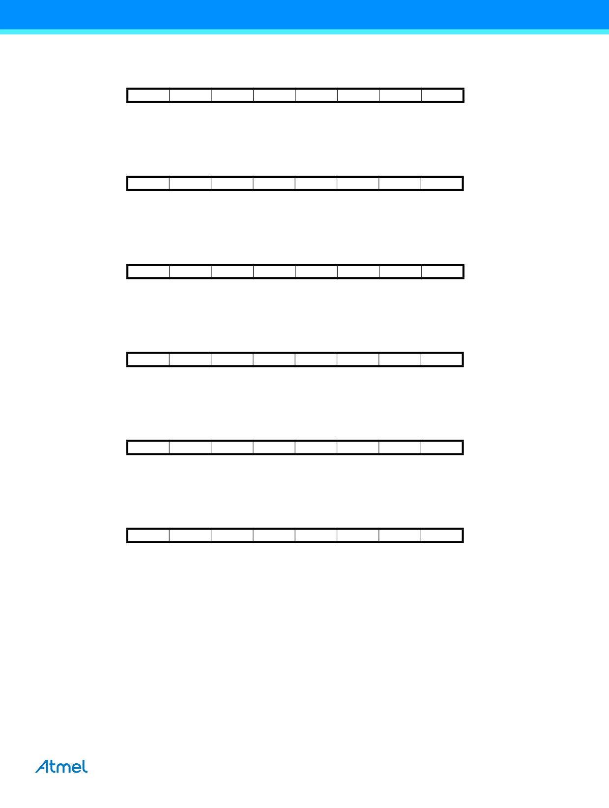
13.4.5
PORTC - The Port C Data Register
Bit
7
6
5
4
3
2
1
0
0x08 (0x28)
-
PORTC6
PORTC5
PORTC4
PORTC3
PORTC2
PORTC1
PORTC0
PORTC
Read/Write
R
R/W
R/W
R/W
R/W
R/W
R/W
R/W
Initial Value
0
0
0
0
0
0
0
0
13.4.6
DDRC - The Port C Data Direction Register
Bit
7
6
5
4
3
2
1
0
0x07 (0x27)
-
DDC6
DDC5
DDC4
DDC3
DDC2
DDC1
DDC0
DDRC
Read/Write
R
R/W
R/W
R/W
R/W
R/W
R/W
R/W
Initial Value
0
0
0
0
0
0
0
0
13.4.7
PINC - The Port C Input Pins Address
Bit
7
6
5
4
3
2
1
0
0x06 (0x26)
-
PINC6
PINC5
PINC4
PINC3
PINC2
PINC1
PINC0
PINC
Read/Write
R
R
R
R
R
R
R
R
Initial Value
0
N/A
N/A
N/A
N/A
N/A
N/A
N/A
13.4.8
PORTD - The Port D Data Register
Bit
7
6
5
4
3
2
1
0
0x0B (0x2B)
PORTD7
PORTD6
PORTD5
PORTD4
PORTD3
PORTD2
PORTD1
PORTD0
PORTD
Read/Write
R/W
R/W
R/W
R/W
R/W
R/W
R/W
R/W
Initial Value
0
0
0
0
0
0
0
0
13.4.9
DDRD - The Port D Data Direction Register
Bit
7
6
5
4
3
2
1
0
0x0A (0x2A)
DDD7
DDD6
DDD5
DDD4
DDD3
DDD2
DDD1
DDD0
DDRD
Read/Write
R/W
R/W
R/W
R/W
R/W
R/W
R/W
R/W
Initial Value
0
0
0
0
0
0
0
0
13.4.10 PIND - The Port D Input Pins Address
Bit
7
6
5
4
3
2
1
0
0x09 (0x29)
PIND7
PIND6
PIND5
PIND4
PIND3
PIND2
PIND1
PIND0
PIND
Read/Write
R
R
R
R
R
R
R
R
Initial Value
N/A
N/A
N/A
N/A
N/A
N/A
N/A
N/A
ATmega328P [DATASHEET]
73
7810D-AVR-01/15
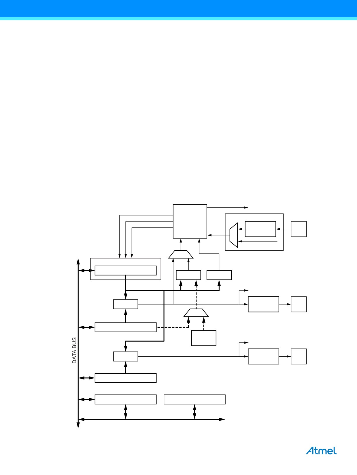
14.
8-bit Timer/Counter0 with PWM
14.1
Features
● Two independent output compare units
● Double buffered output compare registers
● Clear timer on compare match (auto reload)
● Glitch free, phase correct pulse width modulator (PWM)
● Variable PWM period
● Frequency generator
● Three independent interrupt sources (TOV0, OCF0A, and OCF0B)
14.2
Overview
Timer/Counter0 is a general purpose 8-bit Timer/Counter module, with two independent output compare units, and with
PWM support. It allows accurate program execution timing (event management) and wave generation.
A simplified block diagram of the 8-bit Timer/Counter is shown in Figure 14-1. For the actual placement of I/O pins, refer to
Section 1-1 “Pinout” on page 3. CPU accessible I/O registers, including I/O bits and I/O pins, are shown in bold.
The device-specific I/O register and bit locations are listed in the Section 14.9 “Register Description” on page 84.
The PRTIM0 bit in Section 9.10 “Minimizing Power Consumption” on page 36 must be written to zero to enable
Timer/Counter0 module.
Figure 14-1.
8-bit Timer/Counter Block Diagram
TOVn (Int. Req.)
Count
Clear
Clock Select
Control Logic
Direction
Edge
Tn
clkTn
Detector
(from Prescaler)
TOP
BOTTOM
Timer/Counter
TCNTn
=
= 0
OCnA (Int. Req.)
Waveform
=
OCnA
Generation
OCRnA
Fixed
TOP
Value
OCnB (Int. Req.)
Waveform
=
OCnB
Generation
OCRnB
TCCRnA
TCCRnB
74
ATmega328P [DATASHEET]
7810D-AVR-01/15
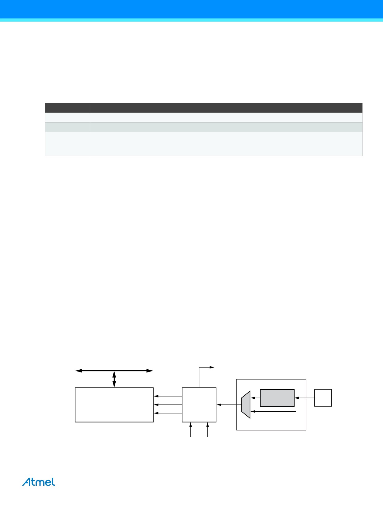
14.2.1
Definitions
Many register and bit references in this section are written in general form. A lower case “n” replaces the Timer/Counter
number, in this case 0. A lower case “x” replaces the output compare unit, in this case compare unit A or compare unit B.
However, when using the register or bit defines in a program, the precise form must be used, i.e., TCNT0 for accessing
Timer/Counter0 counter value and so on.
The definitions in Table 14-1 are also used extensively throughout the document.
Table 14-1. Definitions
Parameter
Definition
BOTTOM
The counter reaches the BOTTOM when it becomes 0x00.
MAX
The counter reaches its MAXimum when it becomes 0xFF (decimal 255).
The counter reaches the TOP when it becomes equal to the highest value in the count sequence. The
TOP
TOP value can be assigned to be the fixed value 0xFF (MAX) or the value stored in the OCR0A register.
The assignment is dependent on the mode of operation.
14.2.2
Registers
The Timer/Counter (TCNT0) and output compare registers (OCR0A and OCR0B) are 8-bit registers. interrupt request
(abbreviated to Int.Req. in the figure) signals are all visible in the timer interrupt flag register (TIFR0). All interrupts are
individually masked with the timer interrupt mask register (TIMSK0). TIFR0 and TIMSK0 are not shown in the figure.
The Timer/Counter can be clocked internally, via the prescaler, or by an external clock source on the T0 pin. The clock select
logic block controls which clock source and edge the Timer/Counter uses to increment (or decrement) its value. The
Timer/Counter is inactive when no clock source is selected. The output from the clock select logic is referred to as the timer
clock (clkT0).
The double buffered output compare registers (OCR0A and OCR0B) are compared with the Timer/Counter value at all
times. The result of the compare can be used by the waveform generator to generate a PWM or variable frequency output on
the output compare pins (OC0A and OC0B). See Section 15.7.3 “Using the Output Compare Unit” on page 99 for details.
The compare match event will also set the compare flag (OCF0A or OCF0B) which can be used to generate an output
compare interrupt request.
14.3
Timer/Counter Clock Sources
The Timer/Counter can be clocked by an internal or an external clock source. The clock source is selected by the clock
select logic which is controlled by the clock select (CS02:0) bits located in the Timer/Counter control register (TCCR0B). For
details on clock sources and prescaler, see Section 16. “Timer/Counter0 and Timer/Counter1 Prescalers” on page 114.
14.4
Counter Unit
The main part of the 8-bit Timer/Counter is the programmable bi-directional counter unit. Figure 14-2 shows a block diagram
of the counter and its surroundings.
Figure 14-2. Counter Unit Block Diagram
TOVn
DATA BUS
(Int. Req.)
Clock Select
count
Edge
Tn
clear
clk
Tn
Detector
TCNTn
Control Logic
direction
(from Prescaler)
bottom
top
ATmega328P [DATASHEET]
75
7810D-AVR-01/15
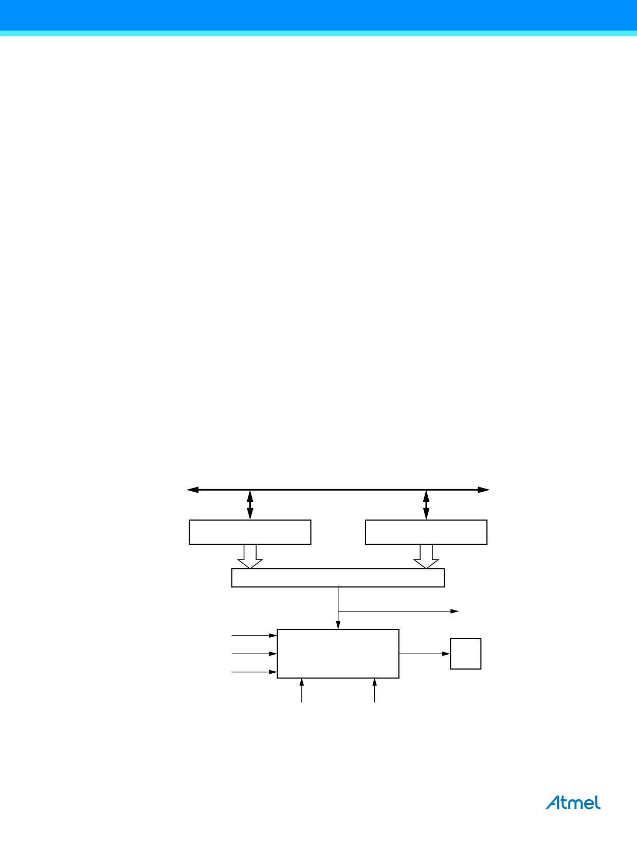
Signal description (internal signals):
count
Increment or decrement TCNT0 by 1.
direction
Select between increment and decrement.
clear
Clear TCNT0 (set all bits to zero).
clkTn
Timer/Counter clock, referred to as clkT0 in the following.
top
Signalize that TCNT0 has reached maximum value.
bottom
Signalize that TCNT0 has reached minimum value (zero).
Depending of the mode of operation used, the counter is cleared, incremented, or decremented at each timer clock (clkT0).
clkT0 can be generated from an external or internal clock source, selected by the clock select bits (CS02:0). When no clock
source is selected (CS02:0 = 0) the timer is stopped. However, the TCNT0 value can be accessed by the CPU, regardless of
whether clkT0 is present or not. A CPU write overrides (has priority over) all counter clear or count operations.
The counting sequence is determined by the setting of the WGM01 and WGM00 bits located in the Timer/Counter control
register (TCCR0A) and the WGM02 bit located in the Timer/Counter control register B (TCCR0B). There are close
connections between how the counter behaves (counts) and how waveforms are generated on the output compare outputs
OC0A and OC0B. For more details about advanced counting sequences and waveform generation, see Section 14.7
“Modes of Operation” on page 78.
The Timer/Counter overflow flag (TOV0) is set according to the mode of operation selected by the WGM02:0 bits. TOV0 can
be used for generating a CPU interrupt.
14.5
Output Compare Unit
The 8-bit comparator continuously compares TCNT0 with the output compare registers (OCR0A and OCR0B). Whenever
TCNT0 equals OCR0A or OCR0B, the comparator signals a match. A match will set the output compare flag (OCF0A or
OCF0B) at the next timer clock cycle. If the corresponding interrupt is enabled, the output compare flag generates an output
compare interrupt. The output compare flag is automatically cleared when the interrupt is executed. Alternatively, the flag
can be cleared by software by writing a logical one to its I/O bit location. The waveform generator uses the match signal to
generate an output according to operating mode set by the WGM02:0 bits and compare output mode (COM0x1:0) bits. The
max and bottom signals are used by the waveform generator for handling the special cases of the extreme values in some
modes of operation (Section 14.7 “Modes of Operation” on page 78).
Figure 14-3 shows a block diagram of the output compare unit.
Figure 14-3. Output Compare Unit, Block Diagram
DATA BUS
OCRnx
TCNTn
= (8-bit Comparator)
OCFnx (Int. Req.)
top
bottom
Waveform Generator
OCnx
FOCn
WGMn1:0
COMnx1:0
76
ATmega328P [DATASHEET]
7810D-AVR-01/15
The OCR0x registers are double buffered when using any of the pulse width modulation (PWM) modes. For the normal and
clear timer on compare (CTC) modes of operation, the double buffering is disabled. The double buffering synchronizes the
update of the OCR0x compare registers to either top or bottom of the counting sequence. The synchronization prevents the
occurrence of odd-length, non-symmetrical PWM pulses, thereby making the output glitch-free.
The OCR0x register access may seem complex, but this is not case. When the double buffering is enabled, the CPU has
access to the OCR0x buffer register, and if double buffering is disabled the CPU will access the OCR0x directly.
14.5.1
Force Output Compare
In non-PWM waveform generation modes, the match output of the comparator can be forced by writing a one to the force
output compare (FOC0x) bit. Forcing compare match will not set the OCF0x flag or reload/clear the timer, but the OC0x pin
will be updated as if a real compare match had occurred (the COM0x1:0 bits settings define whether the OC0x pin is set,
cleared or toggled).
14.5.2
Compare Match Blocking by TCNT0 Write
All CPU write operations to the TCNT0 register will block any compare match that occur in the next timer clock cycle, even
when the timer is stopped. This feature allows OCR0x to be initialized to the same value as TCNT0 without triggering an
interrupt when the Timer/Counter clock is enabled.
14.5.3
Using the Output Compare Unit
Since writing TCNT0 in any mode of operation will block all compare matches for one timer clock cycle, there are risks
involved when changing TCNT0 when using the output compare unit, independently of whether the Timer/Counter is running
or not. If the value written to TCNT0 equals the OCR0x value, the compare match will be missed, resulting in incorrect
waveform generation. Similarly, do not write the TCNT0 value equal to BOTTOM when the counter is down counting.
The setup of the OC0x should be performed before setting the data direction register for the port pin to output. The easiest
way of setting the OC0x value is to use the force output compare (FOC0x) strobe bits in normal mode. The OC0x registers
keep their values even when changing between waveform generation modes.
Be aware that the COM0x1:0 bits are not double buffered together with the compare value. Changing the COM0x1:0 bits will
take effect immediately.
14.6
Compare Match Output Unit
The compare output mode (COM0x1:0) bits have two functions. The waveform generator uses the COM0x1:0 bits for
defining the output compare (OC0x) state at the next compare match. Also, the COM0x1:0 bits control the OC0x pin output
source. Figure 14-4 on page 78 shows a simplified schematic of the logic affected by the COM0x1:0 bit setting. The I/O
registers, I/O bits, and I/O pins in the figure are shown in bold. Only the parts of the general I/O port control registers (DDR
and PORT) that are affected by the COM0x1:0 bits are shown. When referring to the OC0x state, the reference is for the
internal OC0x register, not the OC0x pin. If a system reset occur, the OC0x register is reset to “0”.
ATmega328P [DATASHEET]
77
7810D-AVR-01/15
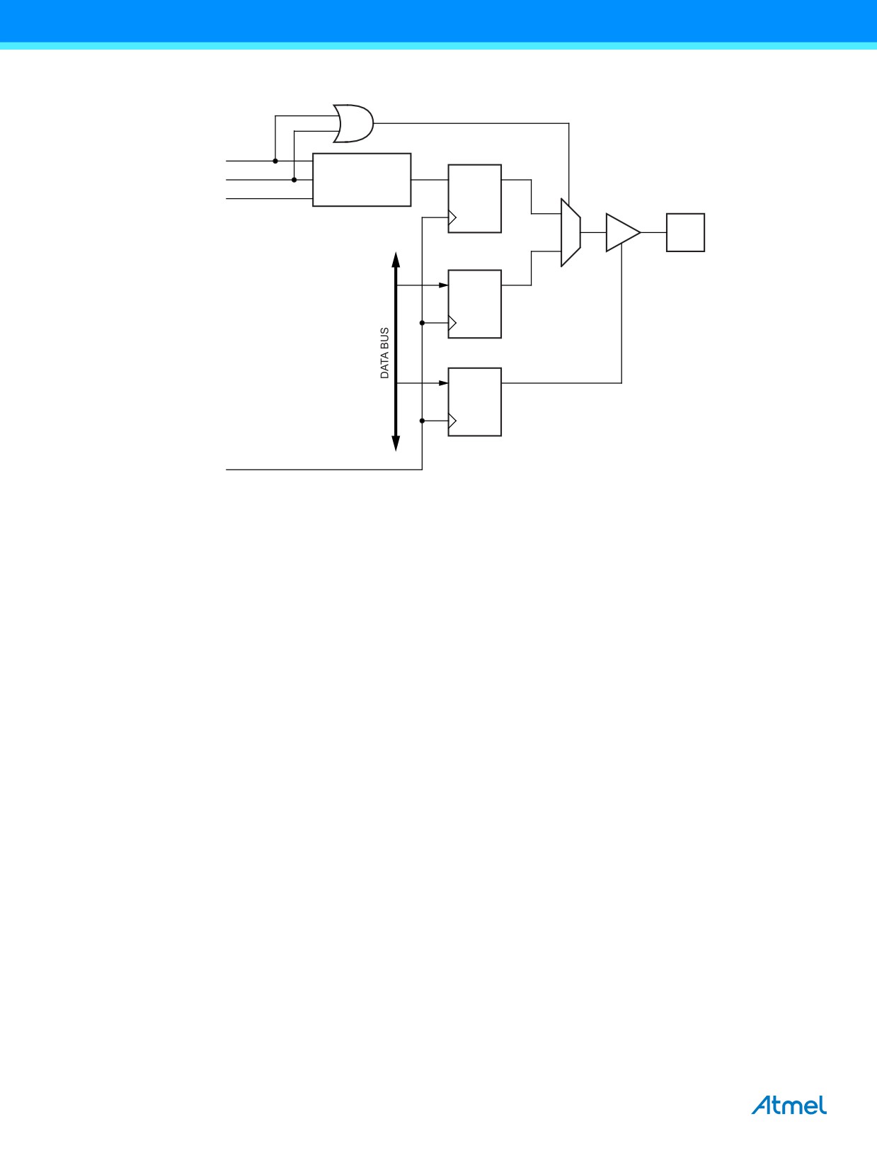
Figure 14-4. Compare Match Output Unit, Schematic
COMnx1
COMnx0
Waveform
D
Q
Generator
FOCnx
1
OCnx
OCnx
Pin
0
D
Q
PORT
D
Q
DDR
clkI/O
The general I/O port function is overridden by the output compare (OC0x) from the waveform generator if either of the
COM0x1:0 bits are set. However, the OC0x pin direction (input or output) is still controlled by the data direction register
(DDR) for the port pin. The data direction register bit for the OC0x pin (DDR_OC0x) must be set as output before the OC0x
value is visible on the pin. The port override function is independent of the waveform generation mode.
The design of the output compare pin logic allows initialization of the OC0x state before the output is enabled. Note that
some COM0x1:0 bit settings are reserved for certain modes of operation. See Section 14.9 “Register Description” on page
84
14.6.1
Compare Output Mode and Waveform Generation
The waveform generator uses the COM0x1:0 bits differently in normal, CTC, and PWM modes. For all modes, setting the
COM0x1:0 = 0 tells the waveform generator that no action on the OC0x register is to be performed on the next compare
match. For compare output actions in the non-PWM modes refer to Table 14-2 on page 84. For fast PWM mode, refer to
Table 14-3 on page 84, and for phase correct PWM refer to Table 14-4 on page 84.
A change of the COM0x1:0 bits state will have effect at the first compare match after the bits are written. For non-PWM
modes, the action can be forced to have immediate effect by using the FOC0x strobe bits.
14.7
Modes of Operation
The mode of operation, i.e., the behavior of the Timer/Counter and the output compare pins, is defined by the combination of
the waveform generation mode (WGM02:0) and compare output mode (COM0x1:0) bits. The compare output mode bits do
not affect the counting sequence, while the waveform generation mode bits do. The COM0x1:0 bits control whether the
PWM output generated should be inverted or not (inverted or non-inverted PWM). For non-PWM modes the COM0x1:0 bits
control whether the output should be set, cleared, or toggled at a compare match (see Section 14.6 “Compare Match Output
Unit” on page 77).
For detailed timing information refer to Section 14.8 “Timer/Counter Timing Diagrams” on page 82.
78
ATmega328P [DATASHEET]
7810D-AVR-01/15
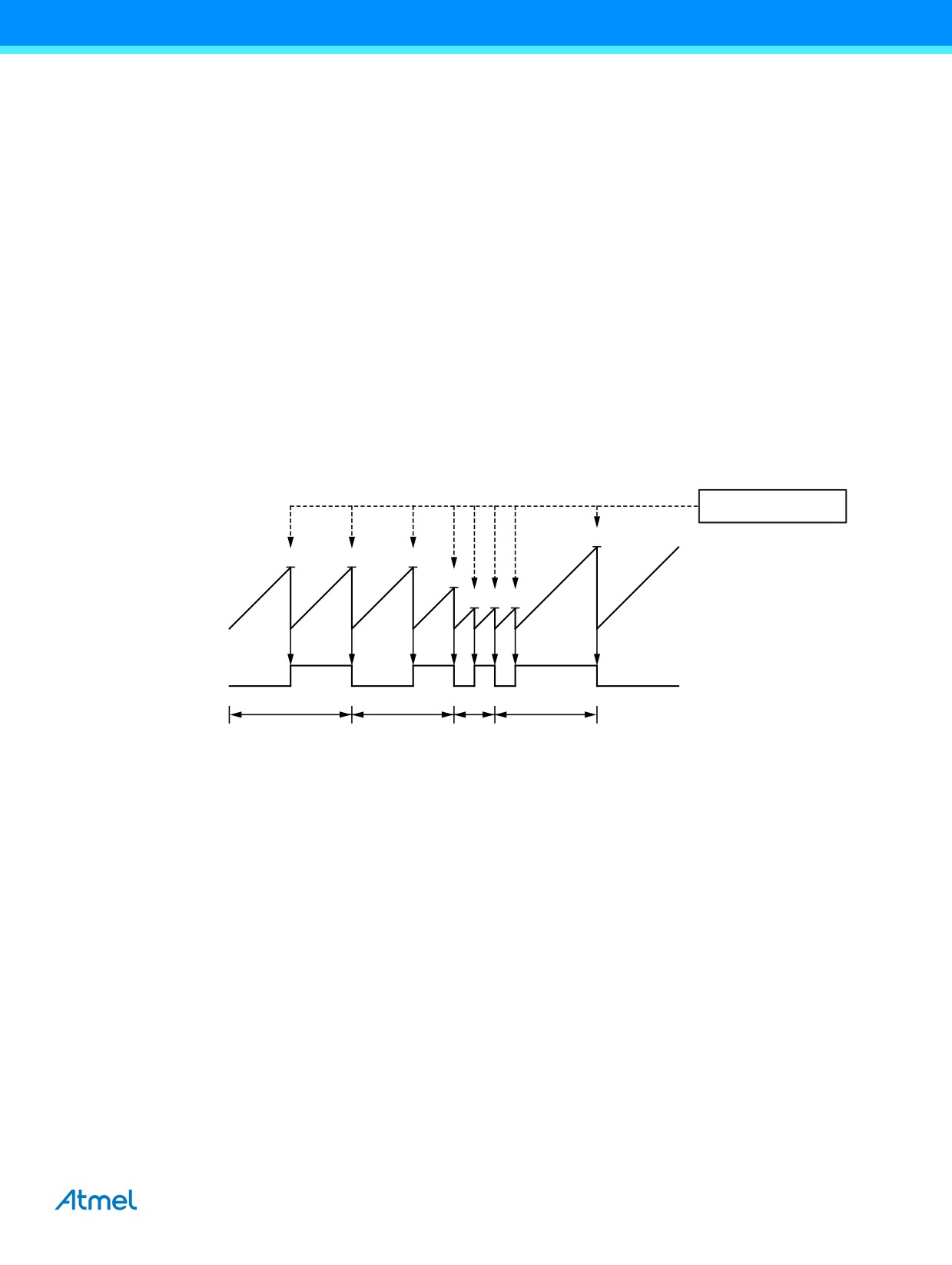
14.7.1
Normal Mode
The simplest mode of operation is the normal mode (WGM02:0 = 0). In this mode the counting direction is always up
(incrementing), and no counter clear is performed. The counter simply overruns when it passes its maximum 8-bit value
(TOP = 0xFF) and then restarts from the bottom (0x00). In normal operation the Timer/Counter overflow flag (TOV0) will be
set in the same timer clock cycle as the TCNT0 becomes zero. The TOV0 Flag in this case behaves like a ninth bit, except
that it is only set, not cleared. However, combined with the timer overflow interrupt that automatically clears the TOV0 flag,
the timer resolution can be increased by software. There are no special cases to consider in the normal mode, a new counter
value can be written anytime.
The output compare unit can be used to generate interrupts at some given time. Using the output compare to generate
waveforms in normal mode is not recommended, since this will occupy too much of the CPU time.
14.7.2
Clear Timer on Compare Match (CTC) Mode
In clear timer on compare or CTC mode (WGM02:0 = 2), the OCR0A register is used to manipulate the counter resolution. In
CTC mode the counter is cleared to zero when the counter value (TCNT0) matches the OCR0A. The OCR0A defines the top
value for the counter, hence also its resolution. This mode allows greater control of the compare match output frequency. It
also simplifies the operation of counting external events.
The timing diagram for the CTC mode is shown in Figure 14-5. The counter value (TCNT0) increases until a compare match
occurs between TCNT0 and OCR0A, and then counter (TCNT0) is cleared.
Figure 14-5. CTC Mode, Timing Diagram
OCnx Interrupt Flag Set
TCNTn
OCn
(COMnA1:0 = 1)
(Toggle)
1
2
3
4
Period
An interrupt can be generated each time the counter value reaches the TOP value by using the OCF0A flag. If the interrupt
is enabled, the interrupt handler routine can be used for updating the TOP value. However, changing TOP to a value close to
BOTTOM when the counter is running with none or a low prescaler value must be done with care since the CTC mode does
not have the double buffering feature. If the new value written to OCR0A is lower than the current value of TCNT0, the
counter will miss the compare match. The counter will then have to count to its maximum value (0xFF) and wrap around
starting at 0x00 before the compare match can occur.
For generating a waveform output in CTC mode, the OC0A output can be set to toggle its logical level on each compare
match by setting the compare output mode bits to toggle mode (COM0A1:0 = 1). The OC0A value will not be visible on the
port pin unless the data direction for the pin is set to output. The waveform generated will have a maximum frequency of
fOC0 = fclk_I/O/2 when OCR0A is set to zero (0x00). The waveform frequency is defined by the following equation:
fclk_I/O
fOCnx
= ----------------------------------------------------
2 N 1 + OCRnx
The N variable represents the prescale factor (1, 8, 64, 256, or 1024).
As for the normal mode of operation, the TOV0 flag is set in the same timer clock cycle that the counter counts from MAX to
0x00.
ATmega328P [DATASHEET]
79
7810D-AVR-01/15