FLUKE 45 Dual Display Multimeter. Service Manual (For IEC 1010 Meters Only) - page 3
Chapter 6
List of Replaceable Parts
Title
Page
6-1.
Introduction
6-3
6-2.
How to Obtain Parts
6-3
6-3.
How to Contact Fluke
6-4
6-4.
Manual Status Information
6-4
6-5.
Newer Instruments
6-4
6-6.
Parts
6-4
6-1
List of Replaceable Parts
Introduction
6
6-1.
Introduction
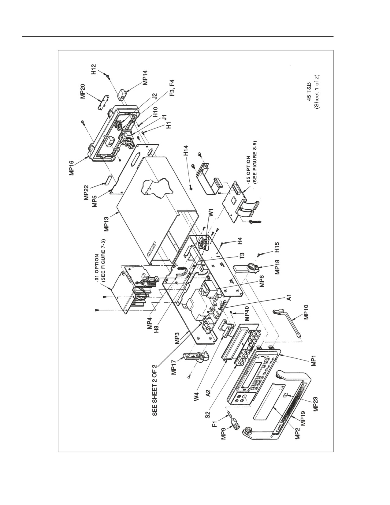
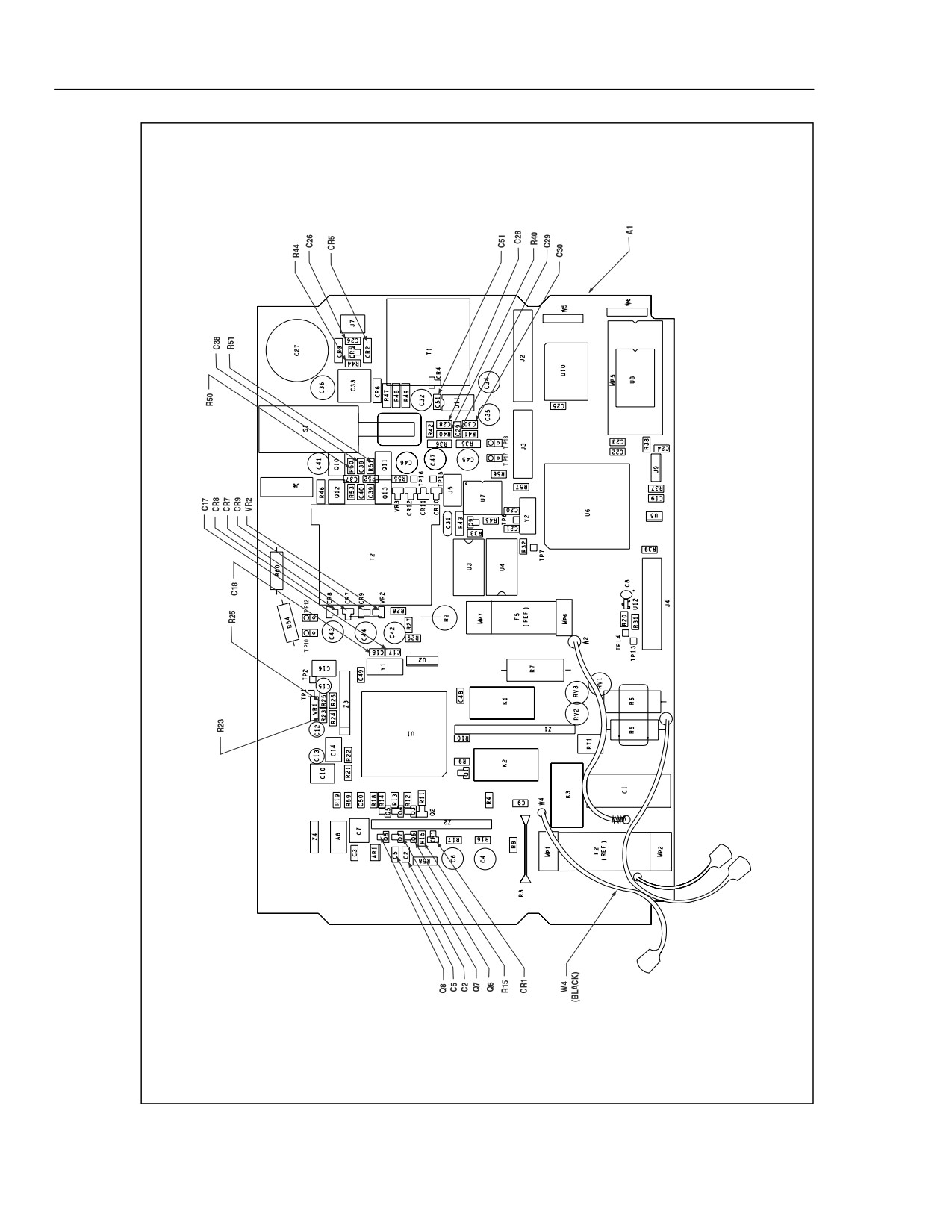
This chapter contains an illustrated list of replaceable parts for the Fluke 45 Dual
Display Multimeter. Parts are listed by assembly; alphabetized by reference designator.
Each assembly is accompanied by an illustration showing the location of each part and
its reference designator. The parts lists give the following information:
• Reference designator
• An indication if the part is subject to damage by static discharge
• Description
• Fluke stock number
• Total quantity
• Any special notes (i.e., factory-selected part)
Caution
A * symbol indicates a device that may be damaged by static
discharge.
6-2.
How to Obtain Parts
Electrical components may be ordered directly from the manufacturer by using the
manufacturers part number, or from the Fluke Corporation and its authorized
representatives by using the part number under the heading FLUKE STOCK NO.
Parts price information is available from the Fluke Corporation or its representatives.
Prices are also available in a Fluke Replacement Parts Catalog which is available on
request.
In the event that the part ordered has been replaced by a new or improved part, the
replacement will be accompanied by an explanatory note and installation instructions, if
necessary.
To ensure prompt delivery of the correct part, include the following information when
you place an order:
• Instrument model and serial number
• Part number and revision level of the pca containing the part.
• Reference designator
• Fluke stock number
• Description (as given under the DESCRIPTION heading)
• Quantity
6-3
45
Service Manual
6-3. How to Contact Fluke
telephone numbers:
USA and Canada: 1-888-99-FLUKE (1-888-993-5853)
Europe: +31 402-675-200
Japan: +81-3-3434-0181
Singapore: +65-738-5655
Anywhere in the world: +1-425-446-5500
6-4. Manual Status Information
The Manual Status Information in Table 6-1 defines the assembly revision levels that are
documented in the manual. Revision levels are printed on the component side of each
PCA.
Table 6-1. Manual Status Information
Ref or
Assembly Name
Fluke Part No.
PCA Revision Levels
Option
No.
A1
Main PCA
814137
AB
A1A1
True Rms PCA
848200
H
A2
Display PCA
609179
A
-01
Battery PCA
825885
A
-05
IEEE-488 Interface PCA
814152
B
6-5. Newer Instruments
Changes and improvements made to the instrument are identified by incrementing the
revision letter marked on the affected pca. These changes are documented on a manual
supplement which, when applicable, is included with the manual.
6-6. Parts
The following pages give detailed listings of Fluke 45 parts.
Note
This instrument may contain a Nickel-Cadmium battery. Do not mix with
the solid waste stream. Spent batteries should be disposed of by a qualified
recycler or hazardous materials handler. Contact your authorized Fluke
service center for recycling information.
6-4

List of Replaceable Parts
Parts
6
Table 6-2. Final Assembly
Reference
Description
Fluke
Total
Note
Designator
Stock
Qty
No.
A
1
MAIN PCA
814137
1
A
2
DISPLAY PCA
609179
1
F
1
FUSE,5X20MM, .500A, 250V, FAST
838151
1
F
2
FUSE,.406X1.5,FAST,11A,1000V,FAST
943118
1
F
3, 4
FUSE,5X20MM,0.125A,250V,SLOW
822254
2
F
5
FUSE,0.44 A, 1000V, FAST
943121
1
H
1, 2
CONN ACC,D-SUB,FEMALE SCREWLOCK,.250
844704
2
H
3
NUT,EXT LOCK,STL,6-32,.344OD
152819
1
H
4-7, 14
SCREW,FHU,P,LOCK,SS,6-32,.250
320093
5
H
8
SCREW,PH,P,LOCK,STL,6-32,.250
152140
1
H
9
SCREW,PH,P,THD CUT,STL,4-14,.500
853668
1
H
10, 11
SCREW,TH,P,SS,4-40,.187
721118
2
H
12, 13
SCREW,PH,P,LOCK,MAG SS,6-32,.500
853986
2
H
15, 16
SCREW,FH,P,LOCK,STL,8-32,.375
114116
2
J
1
PWR PLUG,PANEL,6.3A,250V,3 WIRE
780817
1
J
2
PWR PLUG PART,FUSE HOLDER
780825
1
MP
1
PAD TRANSFER,FRONT PANEL (CE)
609427
1
MP
2
PAD TRANSFER, WINDOW
835496
1
MP
3
ASSEMBLY, CHASSIS
784793
1
MP
4
GROMMET,EXTRUDED,POLYETHYLENE,.085
854351
1
MP
5
DECAL,REAR PANEL (CE)
609419
1
MP
6
INSULATOR, TRANSFORMER
852413
1
MP
7
SPACER,SNAP,.180 RND,NYL,.125
844845
1
MP
8
STANDOFF, FEMALE
874748
1
MP
9
RECEPTACLE,FUSE
824607
1
MP
10
ROD,POWER SWITCH
784827
1
MP
11
SHIELD,TOP
784819
1
MP
12
SHIELD,BOTTOM
791590
1
MP
13
CASE,OUTER
784769
1
MP
14, 15
CASE,FOOT, BLACK
824433
2
MP
16
BEZEL, REAR
885889
1
MP
17
MOUNTING PLATE,HANDLE(LEFT)
857248
1
MP
18
MOUNTING PLATE,HANDLE(RIGHT)
857243
1
MP
19
HANDLE,PAINTED
848205
1
MP
20
COVER,IEEE
791616
1
MP
23
CALIBRATION SEAL
735274
1
MP
29
TEST LEAD ASSY, TL70A
855820
1
MP
32
LABEL,ADHES,PAPER,,4.750,3.1875
854104
1
MP
38
STANDOFF, MALE
874743
1
MP
40
SCREW, PH, 4-14 312
642931
1
S
1
SWITCH,PUSHBUTTON,DPDT,PUSH-PUSH
836361
1
S
2
KEYPAD,ELASTOMERIC
855994
1
T
3
TRANSF,PWR,35W,90-264VAC,14.6-43VAC
609088
1
TM
1
FLUKE 45 USER MAN, ENGLISH
855981
1
TM
2
FLUKE 45 USER MAN, GERMAN/FRENCH
856034
1
W
1
CABLE ASSY,RS232
848192
1
1
W
2
WIRE ASSY,GROUND
834952
1
W
4
CABLE ASSY,FLAT,20 COND,MICROMOD,3 IN
831578
1
W
5
CORD,LINE,5-15/IEC,3-18AWG,SVT,7.5 FT
284174
1
1. For 250 V order part number 769422.
6-5
45
Service Manual
qb28c.eps
Figure 6-1. Final Assembly
6-6
List of Replaceable Parts
Parts
6
MP6
MP11
U8
F2
F5
S1
MP8
MP12
A1
MP7
H9
MP38
MP10
45 T&B
REF
(Sheet 2 of 2)
qb29c.eps
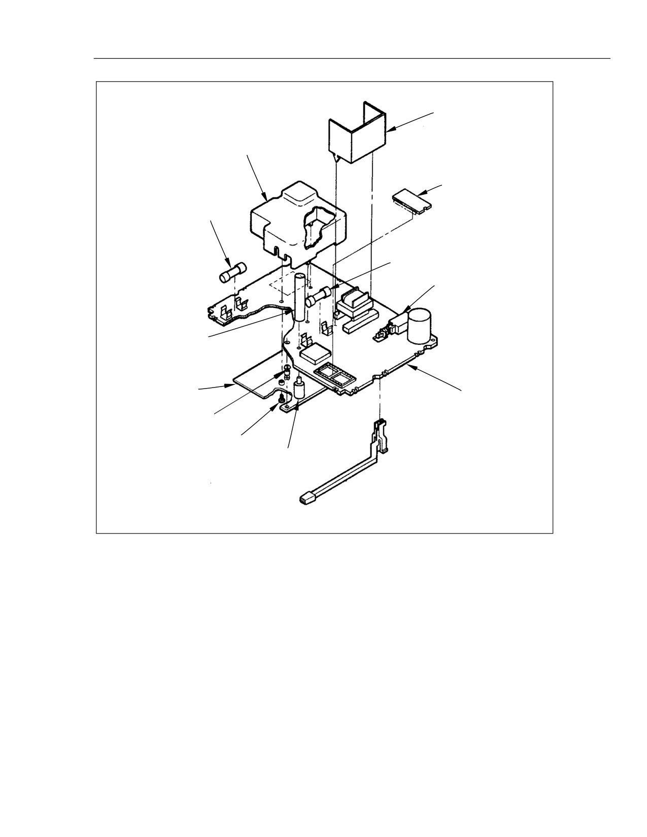
Figure 6-1. Final Assembly (cont)
6-7

45
Service Manual
Table 6-3. A1 Main PCA
Reference
Fluke
Description
Tota
Note
Designator
Stock
l Qty
No.
A
1
TRUE RMS PCA
848200
1
AR
1
I C,OP AMP,JFET INPUT,DECOMP,SOIC
837237
1
C
1
CAP,POLYES,0.1UF,+-10%,1000V
837518
1
C
2
CAP,CER,4.7PF,+-0.25pF,50V,C0G,1206
644978
1
C
3, 5, 9, 19,
CAP,CER,0.1UF,+-10%,25V,X7R,1206
747287
10
C
22-25, 49,
50
C
17, 18
CAP,CER,4.3PF,+-10%,50V,C0G,1206
844738
2
C
4,
6, 42-44
CAP,AL,470UF,+-20%,10V,SOLV PROOF
822387
5
C
7, 10
CAP,POLYES,0.47UF,+-10%,50V
697409
2
C
8
CAP, 2.2µF
697433
1
C
12, 13
CAP,POLYPR,0.12UF,+-10%,50V
851738
2
C
14, 16
CAP,POLYPR,0.033UF,+-10%,63V
721050
2
C
15
CAP,TA,2.2UF,+-10%,35V
697433
1
C
20, 21
CAP,CER,15PF,+-10%,50V,C0G,1206
837393
2
C
26, 37- 40
CAP,CER,0.047UF,+-20%,50V,X7R,1206
782615
5
C
27
CAP,AL,4700UF,+-20%,35V,SOLV PROOF
821553
1
C
28
CAP,CER,33PF,+-10%,50V,C0G,1206
769240
1
C
29, 30
CAP,CER,1800PF,+-10%,50V,C0G,1206
769786
2
C
31
CAP,CER,0.047UF,+-10%,100V,X7R
844733
1
C
32, 36, 47
CAP,AL,10UF,+-20%,63V,SOLV PROOF
816843
3
C
33
CAP,AL,220UF,+-20%,50V,SOLV PROOF
831867
1
C
34, 35,41,
CAP,AL,47UF,+-20%,50V,SOLV PROOF
822403
4
46
C
45
CAP,AL,2.2UF,+-20%,50V,SOLV PROOF
769687
1
C
48
CAP,CER,100PF,+-10%,50V,C0G,1206
740571
1
C
51
CAP,CER,10PF,+-10%,50V,C0G,1206
747311
1
CR
1
DIODE,SI,BV=70.0V,IO=50MA,DUAL,SOT23
742320
1
CR
2,
3
DIODE,SI,100 PIV,1.0 AMP
698555
2
CR
4,
5, 10-12
DIODE,SI,BV=75V,IO=250MA,SOT23
830489
5
CR
6
*
DIODE,SI,SCHOTTKY BARRIER,40V,1A
837732
1
CR
7
DIODE,SI,DUAL,BV=50V,IO=100MA,SOT23
851659
1
CR
8,
9
DIODE,SI,BV=100,IO=100MA,DUAL,SOT23
821116
2
J
2,
4
HEADER,1 ROW,.050CTR,20 PIN
831529
2
J
3
HEADER,1 ROW,.050CTR,14 PIN
831511
1
J
5
HEADER,1 ROW,.100CTR,4 PIN
631184
1
J
6
HEADER,1 ROW,.050CTR,10 PIN
831503
1
J
7
HEADER,1 ROW,.100CTR,3 PIN
845334
1
K
1- 3
RELAY,ARMATURE,2 FORM C,5VDC,LATCH
603001
3
MP
1,
2
CONTACT,FUSE 15AMP
844287
2
MP
3
SPRING,COIL,COMP,SS,.750,.240
836411
1
MP
5
SOCKET,IC,28 PIN,DUAL WIPE,BEAM TYPE
756353
1
MP
6
CONTACT, FUSE
659524
1
MP
7
CONTACT, FUSE
844287
1
6-8

List of Replaceable Parts
Parts
6
Table 6-3. A1 Main PCA (cont)
Reference
Fluke
Description
Total
Note
Designator
Stock
Qty
No.
Q
1
TRANSISTOR,SI,NPN,SELECT IEBO,SOT-23
821637
1
Q
2- 8
TRANSISTOR,SI,N-JFET,SOT-23
820860
7
Q
9
TRANSISTOR,SI,NPN,SMALL SIGNAL,SOT-23
742676
1
Q
10, 12
TRANSISTOR,SI,PNP,T092
698290
2
Q
11, 13
TRANSISTOR,SI,NPN,SELECTED IEBO,TO-92
685404
2
R
2
RES,WW,10,+-5%,5W,30PPM
822064
1
R
3
RES,WW,.010,+-5%,1W,100PPM
820845
1
R
4, 19, 22
RES,CERM,200K,+-5%,.125W,200PPM,1206
746743
3
R
5
RES,WW,3.5k,+-5%,5W,20 PPM
107695
1
R
6,
7
RES,CERM,100K,+-5%,3W
820811
2
R
8, 16, 17
RES,CERM,22,+-5%,.125W,200PPM,1206
746230
3
R
9,37,38, 59
RES,CERM,10K,+-5%,.125W,200PPM,1206
746610
4
R
10
RES,CERM,100K,+-5%,.125W,200PPM,1206
740548
1
R
11-15,
RES,CERM,47K,+-5%,.125W,200PPM,1206
746685
10
31,39,45,
55, 56
R
18
RES,CERM,1M,+-5%,.125W,200PPM,1206
746826
1
R
20, 27, 29
RES,CERM,200,+-5%,.125W,200PPM,1206
746339
3
R
21
RES,CERM,215K,+-1%,.125W,100PPM,1206
836643
1
R
23
RES,CERM,61.9K,+-1%,.125W,100PPM,1206
821330
1
R
24
RES,CERM,16.9K,+-1%,.125W,100PPM,1206
836635
1
R
25
RES,CERM,13.3K,+-1%,.125W,100PPM,1206
836619
1
R
26
RES,CERM,845,+-1%,.125W,100PPM,1206
821322
1
R
28,32
RES.CHI,CERMET, 1K, ±5%, 1/8W
745992
2
R
30
RES,CF,20K,+-5%, 0.25W
441477
1
R
33
RES,CERM,180,+-5%,.125W,200PPM,1206
746321
1
R
35
RES,CF,220K,+-5%,0.25W
851837
1
R
36
RES,CF,1M,+-5%,0.25W
649970
1
R
40
RES,CERM,470K,+-5%,.125W,200PPM,1206
746792
1
R
41
RES,CERM,10.5K,+-1%,.125W,100PPM,1206
851852
1
R
42
RES,CERM,68.1K,+-1%,.125W,100PPM,1206
851845
1
R
43
RES,CF,10K,+-5%,0.25W
697102
1
R
44
RES,CERM,5.62K,+-1%,.125W,100PPM,1206
837047
1
R
46- 49
RES,CF,0.50,+-5%,0.25W
830646
4
R
50, 53
*
RES,CERM,432,+-1%,.125W,100PPM,1206
811885
2
R
51, 52
RES,CERM,47,+-5%,.125W,200PPM,1206
746263
2
R
54,60
RES, MOX 22M,+-5%,1W, 200 PPM
688887
2
R
57
RES,CERM,910,+-5%,.125W,200PPM,1206
769257
1
R
58
RES,CF,1K,+-5%,0.25W
780585
1
RT
1
THERMISTOR,DISC,POS,1.1K,+-20%,25 C
602995
1
RV
1, 2, 3
VARISTOR,910V,+-10%,1.0 MA
876193
3
6-9

45
Service Manual
Table 6-3. A1 Main PCA (cont)
Reference
Fluke
Designator
Description
Total
Note
Stock
Qty
No.
T
1
INDUCTOR,FXD,DUAL,EE24-25,0.4MH,1.2A
817379
1
T
2
TRANSF,INV,5VDC,30KHZ,6KV ISO,EE375
817395
1
U
1
MERCURY/SATURN, ASSY TESTED PLASTIC
776195
1
U
2
IC,ARRAY,7 NPN DARLINGTON PAIRS,SOIC
821009
1
U
3,
4
ISOLATOR, OPTO, LED, TRANSISTOR
688314
2
U
5
IC,NMOS,64 X 16 BIT EEPROM
822353
1
U
6
IC,CMOS,8-BIT MPU,1 MHZ,256 RAM,PLCC
821298
1
U
7
IC,CMOS,RS232 DRIVER/RECEIVER,SOIC
821538
1
U
8
EPROM, PROGRAMMED 27C512
857797
1
U
9
IC,CMOS,AND-NOR GATES,SOIC
837203
1
U
10
IC,CMOS,8K X 8 STATIC RAM,120NS,SOIC
851795
1
U
11
IC,VOLT REG,ADJ,SWITCHING REGULATOR
821215
1
U
12
IC MICROPROCESSOR RESET CIRCUIT
602920
1
VR
1
ZENER,TESTED
857201
1
VR
2
ZENER,UNCOMP,6.0V,5%,20MA,0.2W,SOT-
837161
1
VR
3
23
837179
1
W
1
ZENER,UNCOMP,5.1V,5%,20MA,0.2W,SOT-
834929
1
W
2
23
834945
1
W
3
WIRE ASSY,(H)
834911
1
W
4
WIRE ASSY,FUSE
834937
1
Y
1
WIRE ASSY,INPUT (10A CUR)
650390
1
Y
2
WIRE ASSY,(L)
570606
1
Z
1
CRYSTAL,3.84MHZ,+-0.05%,HC-18/U
851100
1
Z
2
CRYSTAL,3.6864MHZ,+-0.005%,HC-18U
847363
1
Z
3
RES NET THN F TESTED
833921
1
Z
4
RES NET THK FILM TESTED
849984
1
RES NET THN FILM TESTED
RES NET THK FILM TESTED
1. Fusible resistor. To ensure safety, use exact replacement only.
6-10
List of Replaceable Parts
Parts
6
45-4001
qb30c.eps
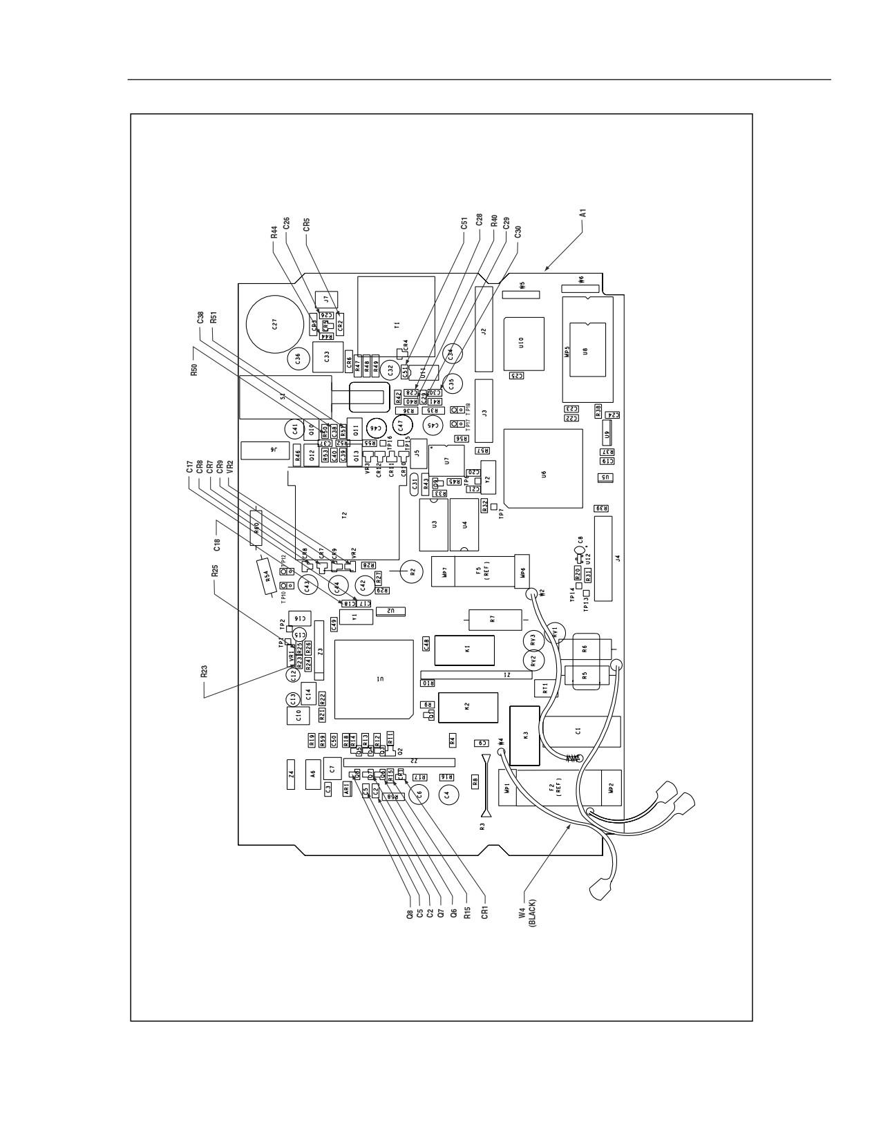
Figure 6-2. A1 Main PCA
6-11
45
Service Manual
Table 6-4. A1A1 True Rms PCA
Fluke
Reference
Description
Tota
Note
Stock
Designator
l Qty
No.
C
1
CAP,TA,2.2UF,+-10%,35V
697433
1
C
2,
3
CAP,TA,68UF,+-20%,6.3V
821785
2
J
1
HEADER,2 ROW,.100CTR,RT ANG,8 PIN
845326
1
R
1
RES,CF,3.3K,+-5%,0.25W
854554
1
U
1
*
IC,BPLR,TRUE RMS TO DC CONVERTER
687019
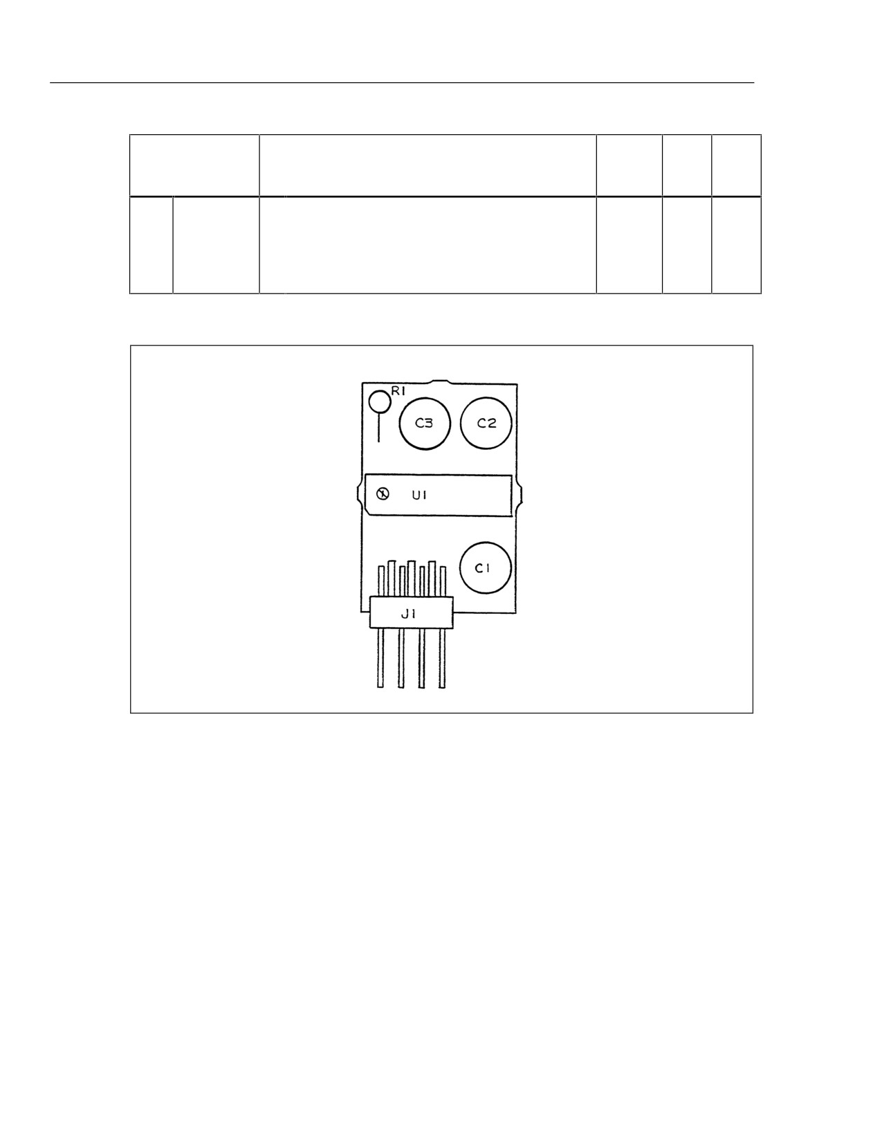
1
45-4006
qb31c.eps
Figure 6-3. A1A1 True Rms PCA
6-12

List of Replaceable Parts
Parts
6
Table 6-5. A2 Display PCA
Reference
Fluke
Description
Total
Note
Designator
Stock
Qty
No.
C
1,
3-
6
CAP,CER,0.1UF,+-10%,25V,X7R,1206
747287
5
C
2
CAP,TA,4.7UF,+-10%,20V
605433
1
CR
3
DIODE,SI,BV=75V,IO=250MA,SOT23
830489
1
DS
1
TUBE,DISPLAY,VAC FLUOR,7&8-SEG,10CHAR
783530
1
J
1
HEADER,1 ROW,.050CTR,20 PIN
831529
1
LS
1
AF TRANSD,PIEZO,22 MM
602490
1
MP 1
1
FLUKE 45-3021, PWB DISPLAY
609161
1
Q
1
TRANSISTOR, SI, PNP, 40V, 300 mW, SOT 23
742684
1
R
1, 10, 12
RES,CERM,10K,+-5%,.125W,200PPM,1206
746610
3
R
2, 5
RES,CERM,2.2M,+-5%,.125W,200PPM,1206
811778
2
R
3
RES,CERM,1.2M,+-5%,.125W,200PPM,1206
806240
1
R
4
RES, CERM,47K,±5%, .125W,220 PPM,1206
746685
1
U
1
IC,CMOS,4-BIT MPU,D75212GF,SMR
688879
1
U
2
RESONATOR, SMR, CERM, 4.19 MHz
688317
1
U
5
IC,CMOS,DUAL MONOSTB MULTIVBRTR,SOIC
806620
1
U
6
*
IC,CMOS,QUAD 2 IN NAND W/SCHMT,SOIC
837245
1
Z
1
RES,CERM,SOIC,16 PIN,15 RES,10K,+-5%
836296
1
6-13
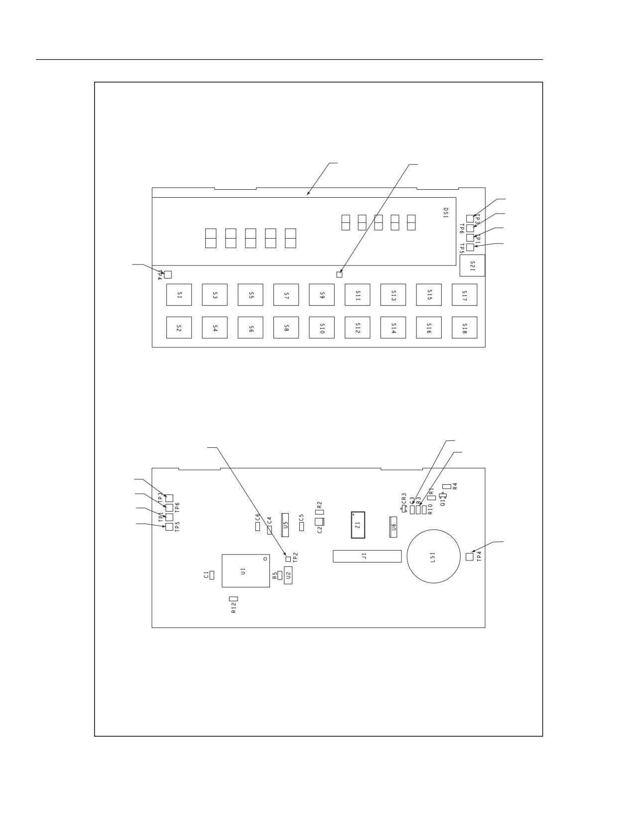
45
Service Manual
DS1
TP2
TP3
TP6
TP1
TP5
TP4
CKT1
C3
TP2
R3
TP3
TP6
TP1
TP5
TP4
CKT2
45-4002
qb32f.eps
Figure 6-4. A2 Display PCA
6-14
Chapter 7
Option -01 Battery Pack
Title
Page
7-1.
Introduction
7-3
7-2.
Specifications
7-3
7-3.
Theory of Operation
7-3
7-4.
Functional Block Description
7-3
7-5.
Switching Power Supply
7-5
7-6.
Cycle/Float Charge Rate Switch
7-5
7-7.
Low Battery Indicator Detector
7-5
7-8.
Low Battery Disconnect
7-5
7-9.
Constant Voltage Trickle Charger
7-6
7-10.
Other Circuits
7-6
7-11. General Maintenance
7-6
7-12.
Removal
7-6
7-13.
Installation
7-7
7-14. Performance Testing
7-9
7-15.
General Operability
7-9
7-16.
Low Battery Indicator Detector and Low Battery Disconnect Test. 7-10
7-17.
Cycle/Float Charge Rate Switch Test
7-10
7-18. Calibration
7-12
7-19. Troubleshooting
7-13
7-20. Additional Tests
7-14
7-21. Schematic Diagram
7-14
7-22. List of Replaceable Parts
7-14
7-1
45
Service Manual
7-2
Option -01 Battery Pack
Introduction
7
7-1.
Introduction
The Fluke 45-01K Battery Kit is a field installable option that may be installed in the
meter. The installation of the Battery Kit facilitates portable operation of the meter for
typically eight hours.
7-2.
Specifications
Specifications for the Battery Kit Option are as follows:
• Type of Cell: Sealed Lead-Acid Rechargeable
• Battery Voltage: 8 Volts Nominal
• Charge Time: 16 Hours Typical w/meter off
7-3.
Theory of Operation
7-4.
Functional Block Description
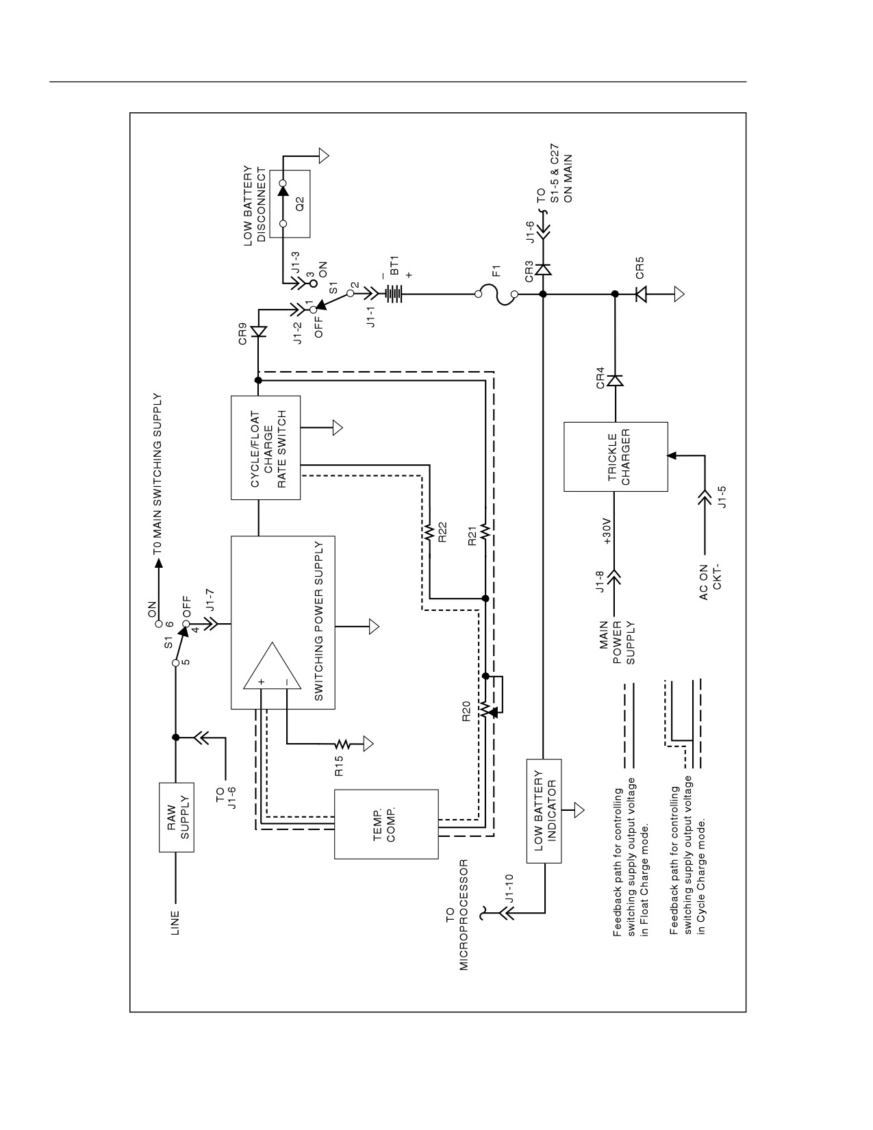
The Battery Pack Option PCA consists of the five functional blocks illustrated in Figure
7-1. Each block is described below:
• Switching Power Supply
The Switching Power Supply regulates the 7.5 V-to-35 V raw dc input provided by
the main circuit board (J1-7). The supply output (9.3 V to 9.8 V, temperature-
compensated) is used to charge the 8 V lead-acid battery.
• Cycle/Float Charge Rate Switch
The Cycle/Float Charge Rate Switch monitors the charging current required by the
battery pack and sets the output voltage accordingly (9.35 V for trickle charging, or
9.8 V for cyclic charging).
• Low Battery Indicator Detector
The Low Battery Indicator Detector monitors the battery pack voltage, outputting a
logic low to turn on the meter low voltage indicator when the battery pack voltage is
below approximately 7.7 V.
• Low Battery Disconnect
The Low Battery Disconnect circuit interrupts meter loading on the battery pack
when battery pack voltage drops below approximately 7.0 V. This action prevents
deep discharge of the batteries.
• Constant Voltage Trickle Charger.
When the meter is operated on line power, the charge on the battery pack is
maintained with the Constant Voltage Trickle Charger (9.25 V output).
7-3
45
Service Manual
qb33f.eps
Figure 7-1. Battery Pack Option Functional Block Diagram
7-4
Option -01 Battery Pack
Theory of Operation
7
7-5.
Switching Power Supply
The switching power supply regulates the output voltage with a pulse-width modulating
technique that varies the on time of the FET switch, Q5. The controller chip for this
process (U4) contains the required 1 V reference, switching oscillator, regulator
comparator, current limit comparators, and output switch. The controller chip is
supported by several external components: C7 sets the oscillator frequency; R17, C6,
and C8 are required for stability; R15, R21, and R20 set the output voltage level. The
variable-width pulse from U4-5 is first level-shifted and clamped by R23, R24, and CR7
and then coupled to the FET switch circuit through inverter U3-2. Hex inverters U3-4,
U3-6, and U3-10 are connected in parallel to provide sufficient drive to the FET gate.
FET switch Q5 is turned on at the beginning of each square wave drive cycle and turned
off at the point necessary to set the desired output voltage.
The current limit is set by the voltage drop across the 0.1-ohm resistance provided by the
parallel configuration of five 0.5-ohm resistors (R29, R34, R35, R36, and R37). Current
limiting occurs when the voltage drop across the ohm resistance is greater than
approximately 100 mV. Current limiting is effected by reducing the duty cycle of the
switching transistor, Q5, which in turn reduces the output voltage of the supply.
A bootstrap supply for the driver and coupling/clamp circuits is provided by CR8, R25,
C9, C11, VR3. The output level has a negative temperature coefficient to provide the
proper charging voltage level for the battery pack over a broad temperature range. This
negative coefficient is provided by the Temperature Compensation circuit (Q4, R18, and
R19) in the feedback path of the switching power supply.
7-6.
Cycle/Float Charge Rate Switch
The Cycle/Float Charge Rate Switch monitors the charging current supplied to the
battery pack during charge when the meter is de-energized. If the current is 60 mA to 80
mA or higher, the charging voltage is increased to about 9.8 V. This level of current
causes a voltage drop across R28 that is sufficient to turn Q6 and Q7 on, connecting one
end of R22 to common. The resulting current through R22 modifies feedback to the
switching supply, causing the increased output voltage.
As the battery pack charge reaches about 90% of capacity, the charge current at 9.8 volts
drops below 60 to 80 mA; Q6 and Q7 turn off, and the charging voltage decreases to
9.35 volts, the trickle charge level for the battery pack. Diode CR10 clamps the voltage
across R28 to about 0.8 V maximum.
7-7.
Low Battery Indicator Detector
The Low Battery Indicator Detector uses comparator U2-7. Bandgap reference VR2 is
connected to the inverting input of the comparator, while the divided-down battery
voltage is connected to the noninverting input. Resistor R16 provides the comparator
with a hysteresis of approximately 0.25 V.
The comparator output is an open collector transistor connected to pull-up resistor R45
on the Main Circuit Assembly. When the battery pack voltage falls below about 7.7 V,
U2-7 goes low. When the battery pack voltage rises above about 8.0 volts, U2-7 goes
high. If the battery pack option is not installed, the pull-up resistor on the Main Circuit
Assembly pulls the battery line high to keep the low battery indicator turned off.
7-8.
Low Battery Disconnect
The Low Battery Disconnect uses FET switch Q2. The FET gate is driven by a latching
circuit comprised of Q3, Q12, Q13, and VR4.
7-5
45
Service Manual
When the power switch is first turned on, a pulse through C15 turns on Q13, which then
turns on Q3. With the Q3 collector voltage now near its emitter voltage and the FET gate
near the battery voltage, the FET switch is on. At the same time, Q12 is turned on; its
collector pulls down the base of Q3, latching the circuit on.
When the voltage between the base of Q12 and the anode of VR4 drops below 6.9 volts
(battery voltage of about 7.0 volts), Q12 cannot be maintained on due to the 6.2 V zener
diode in its emitter circuit, and the circuit unlatches itself. The gate of Q3 then goes to
zero and turns off, disconnecting the battery pack. If the battery pack charge is low, this
circuit does not latch, and the battery pack is protected from being deeply discharged.
7-9.
Constant Voltage Trickle Charger
The Constant Voltage Trickle Charger uses a voltage regulator set at 9.25 volts. The
output voltage is set by the values of R38, R40, and the setting of R39. The 30-volt
supply on the Main Circuit Assembly provides the source for the regulator. Trickle
charging occurs only when the meter is operated on line power.
If trickle charging occurs when the battery pack is low, R2 limits charging current to
about 15 mA maximum.
When the meter is operated solely on battery pack power, the charger is disconnected
from the battery pack. A logic level signal (ACON*) from the Main Circuit Assembly
(J1-5) is maintained high, and the output of comparator U2-1 goes low, pulling U1-1 to
common and setting the U1-2 output at 1.25 volts. CR4 is thus reversed biased,
disconnecting the charger from the battery pack.
7-10.
Other Circuits
During the various modes of operation, switching diodes provide the required battery
pack connections. During battery pack operation of the meter, CR3 connects the battery
pack to the switching supply on the Main Circuit Assembly. During charging (line power
connected), CR5 connects the battery pack to the charging circuit. If line power is
disconnected, CR9 disconnects the battery pack from the charging circuit.
The 5-amp battery pack fuse opens if either the battery pack is connected with the wrong
polarity or if the battery pack output is shorted on the battery pack circuit board.
7-11. General Maintenance
7-12. Removal
Use the following instructions to remove the Battery Pack Option from the meter:
1. Make sure the meter is turned off and unplugged from the power outlet.
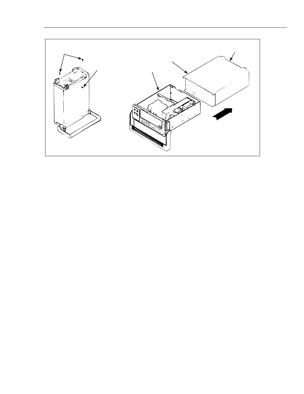
2. Remove the screw from the bottom of the case and the two screws from the rear
bezel (as shown in Figure 7-2 detail A). While holding the front panel, slide the case
and rear bezel off the chassis. (See Figure 7-2 detail B.) At this point, the rear bezel
is not secured to the case.
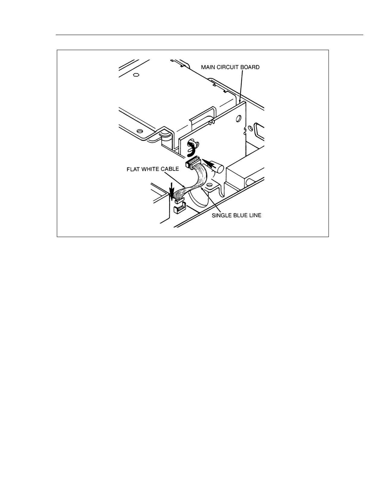
3. Locate the flat white battery pack option cable connector at the Main PCA (see
Figure 7-3.) Use needle nose pliers to detach this connection; alternately pull up on
each end of this connector.
7-6
Option -01 Battery Pack
General Maintenance
7
Rear Bezel
Mounting Screw (2)
Case
Grounding Screw (2)
Chassis
B.
A.
qb14f.eps
Figure 7-2. Removing the Case
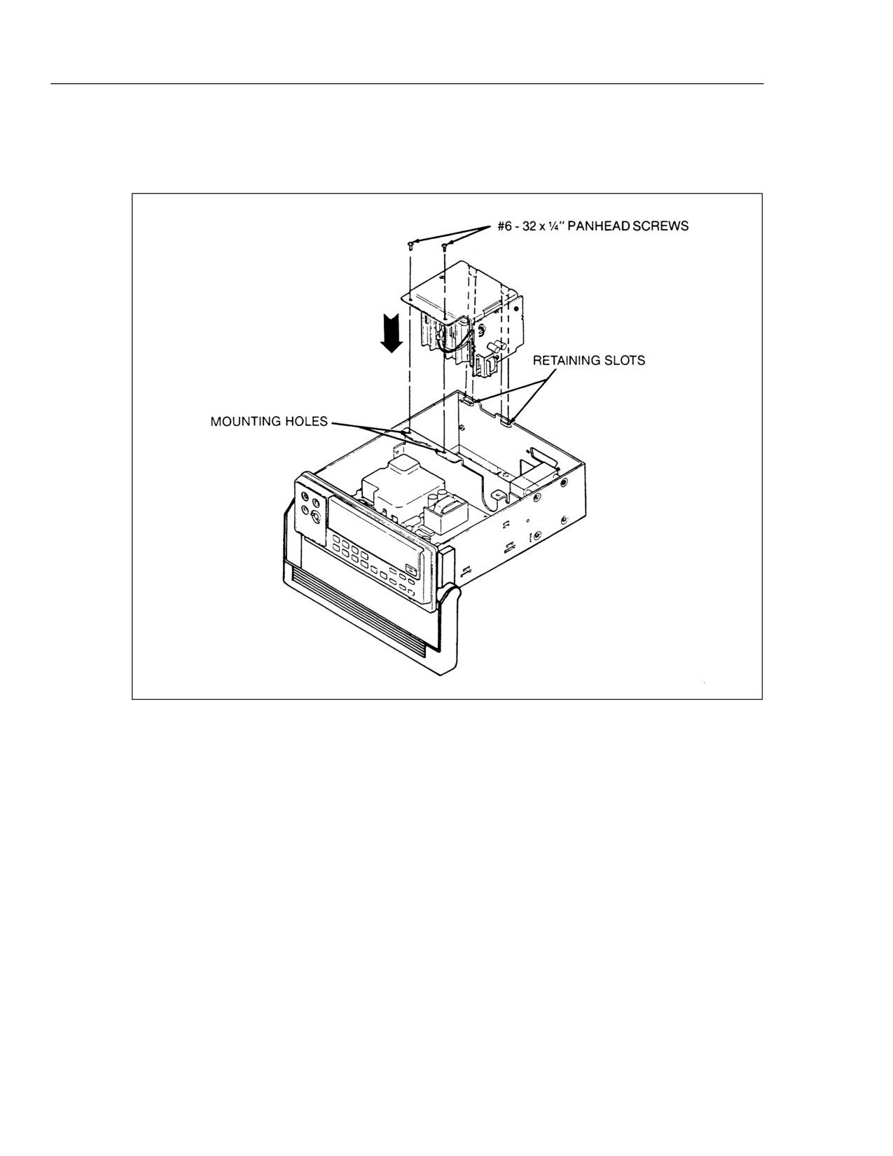
4. Remove the two #6-32 x 1/4" panhead Phillips screws securing the Battery Pack
Option (see Figure 7-4).
5. Carefully slide the Battery Pack Option out of the meter (as shown in Figure 7-4).
Do not pinch the wires running from the circuit board to the battery terminals.
Caution
To prevent damage to the meter when servicing the Main PCA,
unplug the battery pack ribbon cable at the Main PCA or
disconnect the wires to the battery pack.
7-13.
Installation
Use the following instructions to install the Battery Kit Option. Refer to the Instruction
Sheet (PN 856013 - supplied with the Battery Kit) for the more detailed instructions
required with an initial installation of the Battery Kit Option.
1. Make sure the meter is turned off and disconnected from line power.
2. With the meter disconnected from line power, discharge the power supply capacitor
by turning the meter on. After five seconds, turn the meter off.
3. Carefully slide the battery kit into the area reserved for it in the back of the meter (as
shown in Figure 7-4). Make sure that both the retaining slots line up and the
mounting holes mate. Do not pinch wires running from the circuit assembly to the
battery pack terminals.
4. Secure the battery kit with two #6-32 x 1/4" panhead Phillips screws.
5. Attach the flat, white connecting cable at the Battery Pack Option circuit board (see
Figure 7-3). The single blue line of the cable should be to the rear of the meter.
Align the plastic socket on the cable end, then seat it securely in place.
6. Reinstall the meter case to seat properly in the front panel. Attach the rear bezel with
the two panhead Phillips screws, and secure the case with the flathead Phillips screw
in the bottom.
7-7
45
Service Manual
7. To ensure that the battery kit is properly installed, turn the meter ON before
connecting the power cord. If the meter does not turn on, the battery pack may be in
the discharged state. Charge the battery pack for 16 hours; then retest.
qb35c.eps
Figure 7-3. Installing the Battery Kit
7-8
Option -01 Battery Pack
Performance Testing
7
qb34c.eps
Figure 7-4. Battery Pack Option Connecting Cable
7-14. Performance Testing
7-15. General Operability
The following performance verification assumes the following initial setup
configuration:
• The Battery Pack Option is physically installed in the meter.
• The red and black battery pack wires have been disconnected.
Refer to Table 7-1 for description of any equipment that is required during the
performance tests.
1. Disconnect the meter from line power. Now turn meter power on (1 = on), then off
(0 = off).
Note
Do not connect the battery pack until after the option assembly is turned
on later in this procedure.
2. Connect the 1.8 kΩ resistor across the battery pack wires. Connect the voltmeter
(Low to TP1 and High to TP2.)
3. Connect the meter to line voltage, but do not turn the meter on.
4. Check for a voltmeter reading of 9.35 V ±0.01V.
5. Now turn power on. Check for a voltmeter reading of 9.25 V ±0.01 V.
6. Remove the voltmeter and the 1.8 kΩ resistor.
7-9
45
Service Manual
7. Observing the polarity markings on the battery pack, connect the red wire to the
positive (+) terminal. Then connect the black (or brown) wire to the negative (-)
terminal. Reversal of these connections causes fuse F1 to open.
7-16.
Low Battery Indicator Detector and Low Battery Disconnect Test
The following test is necessary only after repairs have been made to either the Low
Battery Indicator Detector or the Low Battery Disconnect circuit.
1.
Turn the meter OFF.
2.
Unplug the two battery pack connectors from the battery pack terminals. Observing
the correct polarity, connect the variable power supply to the two battery pack
connectors.
3.
Connect the voltmeter across the variable power supply.
4.
Set the variable power supply to approximately 9 volts.
5.
Now turn the meter ON, and check for correct operation of the Low Battery
Indicator symbol.
• While watching the display, slowly lower the variable voltage power supply
output. Check that the low battery indicator symbol comes on at 7.7 ±0.25 V dc.
• Now, slowly increase the variable voltage supply output. Check that the low
battery indicator symbol goes out at about 8 V dc.
6.
Check the Low Battery Disconnect point.
• With the meter still operating on the variable supply, slowly lower the voltage,
and check that the meter goes OFF at about 7.0 V dc.
• After the meter goes OFF, slowly increase the voltage, and check that the meter
does not come ON before approximately 8.0 V dc.
Note
The meter may not come on, above 8 volts until the power is cycled.
7.
There are no adjustments to set the Low Battery Indicator point or the Low Battery
Disconnect point.
7-17.
Cycle/Float Charge Rate Switch Test
Use the following procedure to verify operation of the meter's Cycle/Float Charge Rate
Switch. Note that this test is required only after repairs have been performed on the
Cycle/Float Rate Switch Test circuits.
1. Turn the meter OFF.
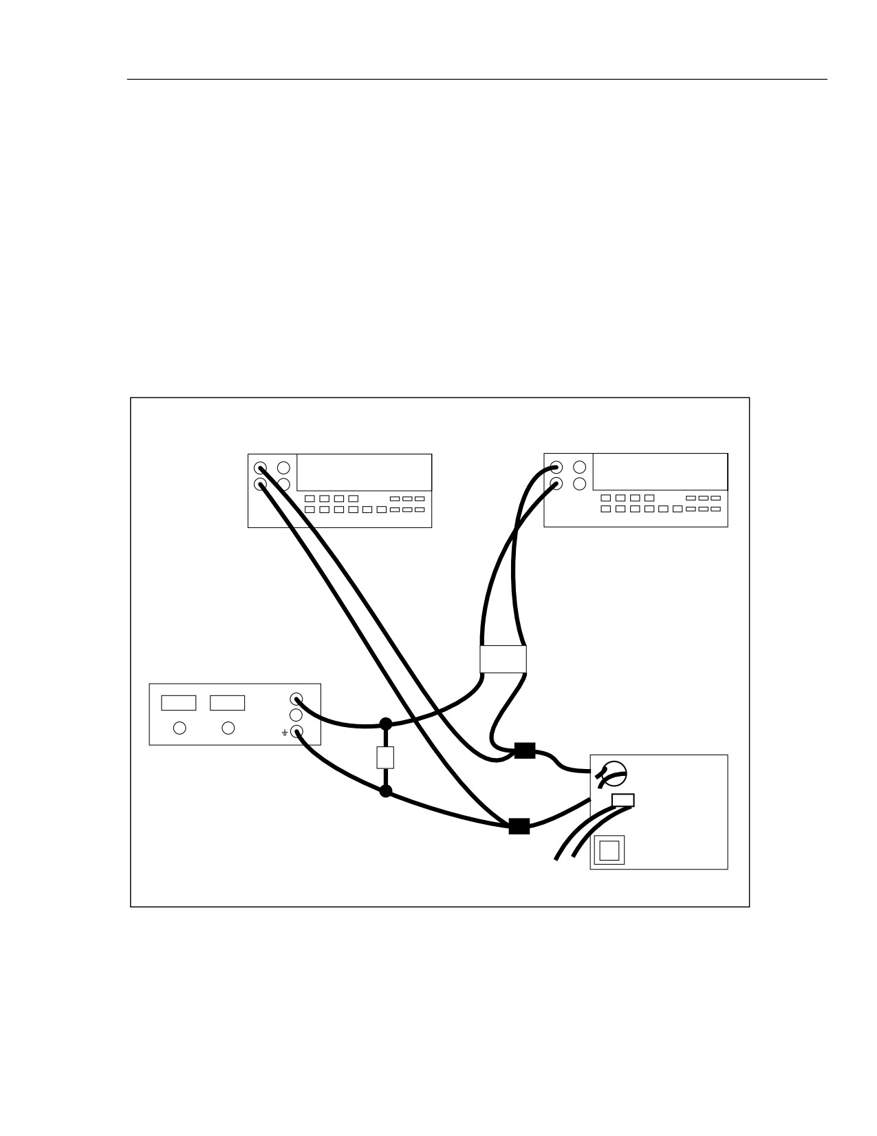
2. For this procedure, use a battery simulator as a substitute for the regular battery
pack. Connect this simulator (shown in Figure 7-5) as follows:
• Connect a 33Ω, 5W load resistor in parallel across the output of a variable
voltage power supply.
• Disconnect the battery charger wires from the battery.
• Connect the simulator to the battery charger wires. Install a 0.1Ω shunt resistor
in series with the red wire.
• Connect a voltmeter across the shunt resistor to measure the voltage drop across
and the charging current through the resistor.
7-10
Option -01 Battery Pack
Calibration
7
3. With no ac line power applied to the meter, adjust the variable voltage power supply
for 8.5 V dc output.
4. Now apply ac line power, and check that the charging current is greater than 250
mA.
5. Slowly increase the variable voltage supply output. Check for the following:
• The charging current decreases as the supply voltage approaches 10 V dc.
• The current should continue to decrease as the voltage increases, until the
current is between 60 and 80 mA.
• With any additional decrease in current (increase of the supply voltage), the
current should suddenly jump to a low value (less than 0.5 mA.)
• When the variable voltage supply output is reduced to 9.35 V dc, the current
should be between 5 and 15 mA.
OPTIONAL VOLTMETER
METER TO MEASURE
TO MONITOR A BATTERY VOLTAGE
CHARGING CURRENT
.1Ω SHUNT
+
V
I
-
RED
POWER SUPPLY
33
Ω
0 TO 15V
5Ω
BLACK
BATTERY OPTION PCA
qb36f.eps
Figure 7-5. Cycle/Float Charge Rate Switch Test
7-11
45
Service Manual
7-18. Calibration
The Battery Pack Option is adjusted at the factory for optimum performance and should
not require adjustment when installed. However, if either of the two adjustment pots on
the top of the Battery Pack Option circuit assembly have been turned inadvertently, or if
the unit has been repaired, the following procedure can be used to reset the controls for
optimum battery life and proper power supply system performance.
The following equipment is needed to perform these adjustments:
• An 1800 Ω, 1/2 watt, 5% resistor
• A voltmeter
The following steps describe how to adjust the Battery Pack Option:
1. With the Battery Pack Option installed in the meter and with the meter disconnected
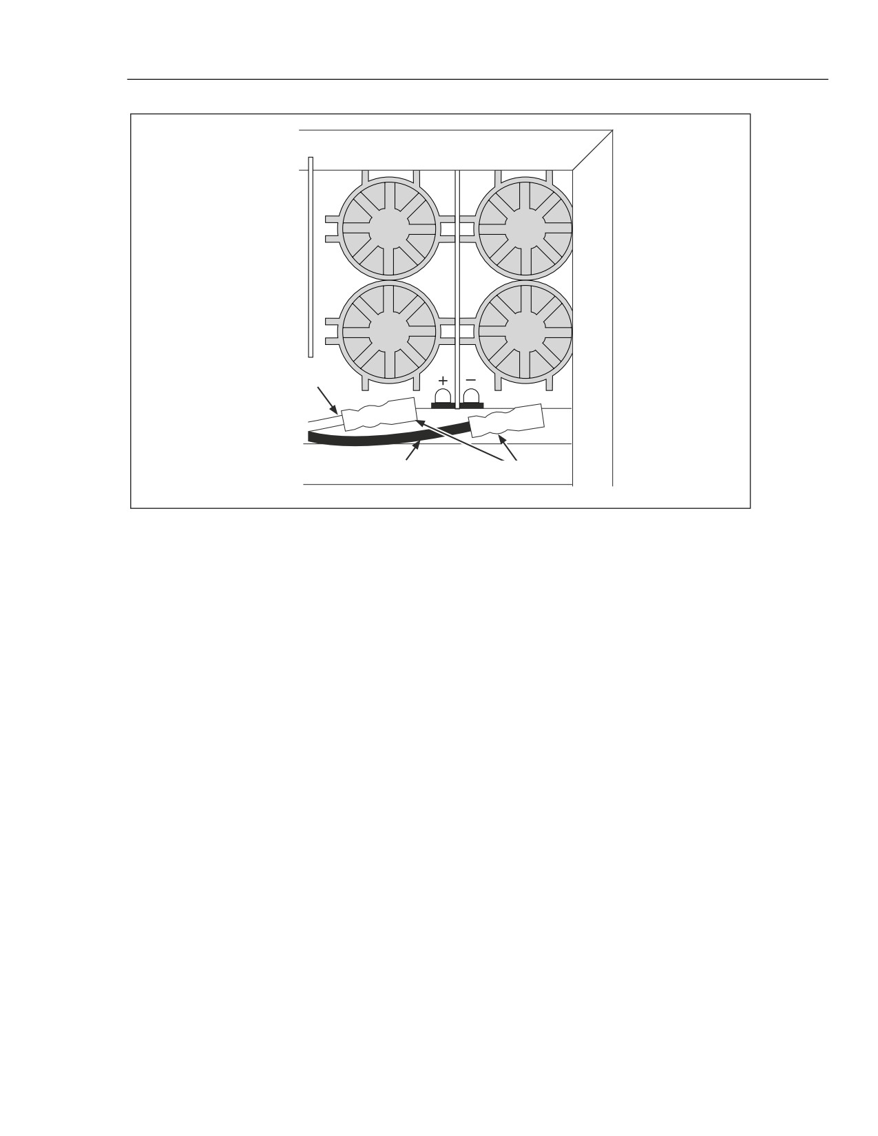
from line power, unplug the battery connectors from the battery + and - terminals
(Figure 7-6).
2. Install the 1800 Ω resistor across the battery pack connectors.
3. Connect the meter to line power and turn the meter ON.
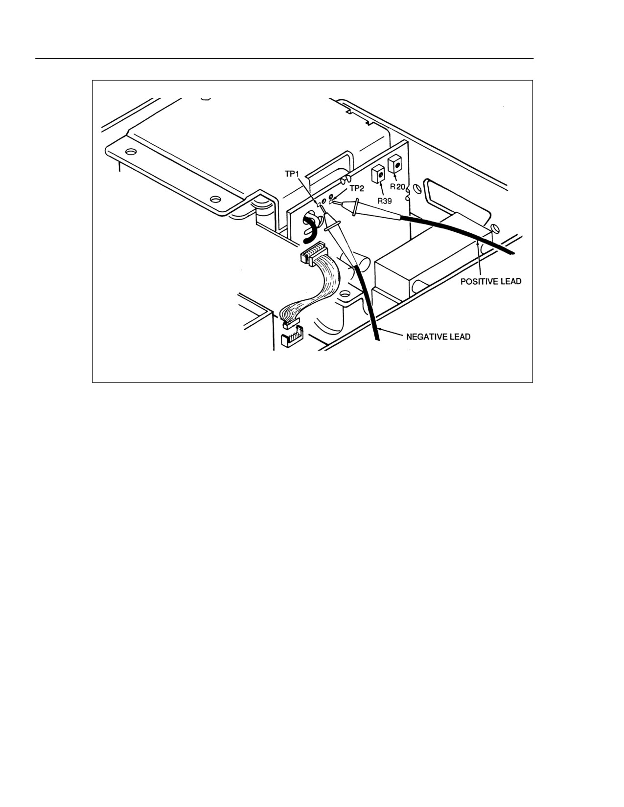
4. Connect the test leads from another voltmeter across test points TP1 and TP2 on the
Battery Pack Option circuit assembly (as shown in Figure 7-7). Adjust the front
potentiometer (R39) (top of the Battery Pack Option circuit assembly) until the
voltmeter across the test points reads 9.25 V.
5. Turn the meter OFF.
6. Connect the test leads from another voltmeter across TP1 and TP2 on the battery
pack option circuit assembly. Adjust rear potentiometer R20 (top of the battery pack
option circuit assembly) until the voltmeter across the test points reads 9.35 volts.
(With the meter connected to line power and turned off, the charging voltage reads
approximately 9.35 volts.)
7. Disconnect the line cord from the meter.
8. Remove the 1800 Ω resistor, and plug the battery pack connector wires back into the
battery pack (the red wire to + and the black wire to -.)
9. To ensure the battery pack connector wires are properly connected and the battery
kit is properly installed, turn the meter ON without plugging in the power cord.
7-12
Option -01 Battery Pack
Troubleshooting
7
View from bottom of instrument
Red
Black
Battery Connectors
qb37f.eps
Figure 7-6. Unplugging the Battery Pack Connectors
7-19. Troubleshooting
Troubleshooting can be facilitated by removing the Battery Pack Option and connecting
the Battery PCA with an extender cable (Fluke Part Number 854245). Refer to the
removal instructions provided earlier in this chapter.
With the meter off (but plugged into line power), check for approximately 16 V dc (at
120V ac line) raw dc supply between the ground test point and the cathode of either
A1CR2 or A1CR3. If necessary, check for transformer secondary voltage of
approximately 24 V ac.
Use an oscilloscope to trace the waveforms associated with the switching power supply.
• With the line voltage at 120 V ac, check the waveform at the drain of FET Q5. This
signal should be a 25 V p-p square wave, with the negative part at zero volts, a
period of 20 to 25 µs, and an ON duty ratio of .20 to .50. This square wave may
exhibit a damped sine wave (two to ten cycles) ringing on the trailing half of the
positive portion. The sine wave amplitude should be from 10 to 20 V p-p.
• Check for a 15 V p-p square wave at the gate of Q5.
• Check for a 14 V p-p square wave at U4-5.
• Check for a 0.5 V p-p sawtooth waveform (with a period of 20 to 25 µs) at U4-3.
Make sure that the oscilloscope is ac-coupled for this measurement.
Troubleshoot other sections of the Battery Pack Option assembly by making dc voltage
measurements. For circuit common, use the GND test point on the main circuit board or
the common end of R30 on the Battery Pack PCA. Note that the battery pack negative
terminal is not connected to common when the low battery disconnect circuit turns off
Q2.
7-13
45
Service Manual
qb38c.eps
Figure 7-7. Test Points and Adjustments
7-20. Additional Tests
The Low Battery Indicator Detector/Low Battery Disconnect Test and the Cycle/Float
Charge Switch Test described earlier under Performance Testing can also be used as
fault isolation aids in troubleshooting the Battery Pack Option.
7-21. Schematic Diagram
The schematic diagram for the Battery Pack Option is included in Chapter 9 of this
manual.
7-22. List of Replaceable Parts
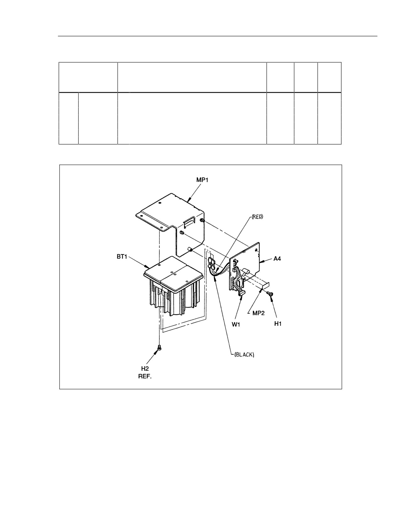
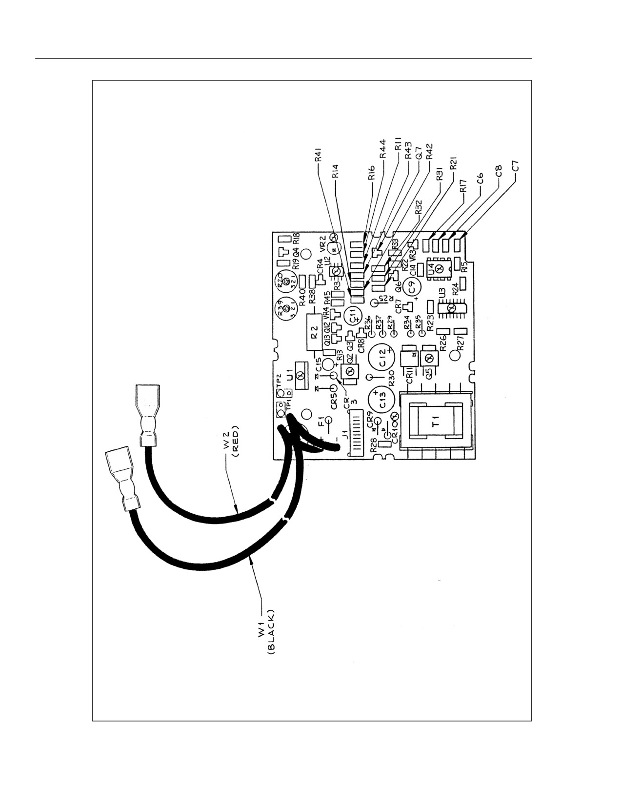
Figures 7-8 and 7-9 provide illustration for parts list in Tables 7-2 and 7-3, respectively.
Refer to Chapter 6 for parts ordering information.
7-14
Option -01 Battery Pack
List of Replaceable Parts
7
Table 7-1. Option -01 Battery Pack Final Assembly
Reference
Description
Fluke
Total
Note
Designator
Stock
Qty.
No.
A
4
*
BATTERY PCA
825885
1
BT
1
BATTERY,LEAD-ACID,8.0V,2.5AH
822262
1
H
1-4
SCREW,PH,P,LOCK,STL,6-32,.250
152140
4
MP
1
RETAINER,BATTERY
828814
1
MP
34
TAPE,FOAM,URETHANE,ADHES,.063,.500
854539
1
TM
1
FLUKE 45 BATTERY KIT INST SHEET
856013
1
W
1
CABLE ASSY,FLAT,10 COND,MICROMOD,3 IN
831552
1
45-01 T&B
qb39c.eps
Figure 7-8. Option-01 Battery Pack Final Assembly
7-15

45
Service Manual
Table 7-2. A4 Battery Pack PCA
Fluke
Total
Reference
Description
Note
Stock
Qty.
Designator
No.
C
6, 7
CAP,CER,1800PF,+-10%,50V,C0G,1206
769786
2
C
8
CAP,CER,33PF,+-10%,50V,C0G,1206
769240
1
C
9
CAP,AL,47UF,+-20%,50V,SOLV PROOF
822403
1
C
11
CAP,AL,10UF,+-20%,63V,SOLV PROOF
816843
1
C
12
CAP,AL,47UF,+-20%,100V,SOLV PROOF
837492
1
C
13
CAP,AL,1000UF,+-20%,16V,SOLV PROOF
837468
1
C
14
CAP,CER,0.22UF,+80-20%,50V,Y5V,1206
740597
1
C
15
CAP,AL,2.2UF,+-20%,50V,SOLV PROOF
769687
1
CR
3, 5, 9
DIODE,SI,SCHOTTKY BARRIER,40V,1A
837732
3
CR
4, 7, 8
DIODE,SI,BV=75V,IO=250MA,SOT23
830489
3
CR
10
DIODE,SI,100 PIV,1.0 AMP
698555
1
CR
11
DIODE,SI,100 PIV,3.3 AMP,SCHOTTKY
837740
1
F
1
FUSE,.095X.28,5A,125V,FAST,AXIAL
696427
1
J
1
HEADER,1 ROW,.050CTR,10 PIN
831503
1
Q
2, 5
TRANSISTOR,SI,NMOS,1W,D-PAK
822106
2
Q
3, 7
TRANSISTOR,SI,PNP,SMALL SIGNAL,SOT-23
742684
2
Q
4, 6, 12, 13
TRANSISTOR,SI,NPN,SMALL SIGNAL,SOT-23
742676
4
R
2
RES,MOX,1.5K,+-5%,1W
603685
1
R
3, 42
RES,CERM,47K,+-5%,.125W,200PPM,1206
746685
2
R
11
RES,CERM,130K,+-5%,.125W,200PPM,1206
851761
1
R
13
RES,CERM,523K,+-1%,.125W,100PPM,1206
844956
1
R
14
RES,CERM,100K,+-1%,.125W,100PPM,1206
769802
1
R
15
RES,CERM,10.5K,+-1%,.125W,100PPM,1206
851852
1
R
16, 43
RES,CERM,10M,+-5%,.125W,300PPM,1206
783274
2
R
17
RES,CERM,470K,+-5%,.125W,200PPM,1206
746792
1
R
18
RES,CERM,330K,+-5%,.125W,200PPM,1206
746776
1
R
19
RES,CERM,51K,+-5%,.125W,200PPM,1206
746693
1
R
20
RES,VAR,CERM,10K,+-20%,0.3W
837559
1
R
21
RES,CERM,59K,+-1%,.125W,100PPM,1206
851803
1
R
22
RES,CERM,301K,+-1%,.125W,100PPM,1206
821652
1
R
23
RES,CERM,470,+-5%,.125W,200PPM,1206
740506
1
R
24
RES,CERM,3.3K,+-5%,.125W,200PPM,1206
746529
1
R
25
RES,METAL FILM,2.26k,+-1%,0.5W
603693
1
R
26, 44
RES,CERM,10,+-5%,.125W,200PPM,1206
746214
2
R
27
RES,CERM,100K,+-5%,.125W,200PPM,1206
740548
1
R
28
RES,CERM,12,+-5%,.125W,200PPM,1206
845458
1
R
29, 34- 37
RES,CF,0.50,+-5%,0.25W
830646
5
R
30
RES,CF,560,+-5%,0.25W
810440
1
R
31
RES,CERM,100,+-5%,.125W,200PPM,1206
746297
1
R
32, 41
RES,CERM,1K,+-5%,.125W,200PPM,1206
745992
2
R
33
RES,CERM,120,+-5%,.125W,200PPM,1206
746305
1
R
38
RES,CERM,910,+-5%,.125W,200PPM,1206
769257
1
R
39
RES,VAR,CERM,200,+-20%,0.3W
837567
1
R
40
RES,CERM,6.8K,+-5%,.125W,200PPM,1206
746024
1
R
45
*
RES,CERM,2.2K,+-5%,.125W,200PPM,1206
746479
1
7-16

Option -01 Battery Pack
List of Replaceable Parts
7
Table 7-2. A4 Battery Pack PCA (cont)
Reference
Fluke
Total
Description
Note
Designator
Stock
Qty.
No.
T
1
INDUCTOR,FXD,DUAL,EE24-25,0.4MH,1.2A
817379
1
U
1
IC,VOLT REG,ADJ,1.2 TO 37 V,1.5 AMPS
460410
1
U
2
IC,COMPARATOR,DUAL,LOW PWR,SOIC
837211
1
U
3
IC,CMOS,HEX BUFFERS,SOIC
837229
1
U
4
IC,VOLT REG,ADJ,SWITCHING REGULATOR
821215
1
VR
2
IC, 1.23V,150 PPM T.C.,BANDGAP V. REF
634451
1
VR
3
ZENER,UNCOMP,15V,5%,8.5MA,0.2W,SOT-23
83787
1
VR
4
*
ZENER,UNCOMP,6.8V,5%,20MA,0.2W,SOT-23
83795
1
W
1
WIRE ASSY,BATTERY,BLACK
834960
1
W
2
WIRE ASSY,BATTERY,RED
844332
1
7-17
45
Service Manual
qb40c.eps
Figure 7-9. A4 Battery Pack PCA
7-18
Chapter 8
Option -05 IEEE-488 Interface
Title
Page
8-1.
Introduction
8-3
8-2.
Theory of Operation
8-3
8-3.
Functional Block Description
8-3
8-4.
Detailed Circuit Description
8-3
8-5.
Main Assembly Connectors
8-3
8-6.
Address Decoding Circuit
8-3
8-7.
Isolation Circuits
8-4
8-8.
IEEE-488 Controller
8-4
8-9.
IEEE-488 Transceivers/Connector
8-5
8-10.
General Maintenance
8-8
8-11.
Removing the IEEE-488 Interface Option
8-8
8-12.
Installing the IEEE-488 Interface Option
8-9
8-13.
Performance Testing
8-9
8-14.
Troubleshooting
8-10
8-15.
Power-up Problems
8-10
8-16.
Communication Problems
8-10
8-17.
Failure to Select IEEE-488 Interface Option
8-10
8-18.
Failure to Handshake on IEEE-488 Bus
8-11
8-19.
Failure to Enter Remote
8-11
8-20.
Failure to Receive Multiple Character Commands
8-12
8-21.
Failure to Transmit Query Responses
8-12
8-22.
Failure to Generate an End or Identify (EOI)
8-12
8-23.
Failure to Generate a Service Request (SRQ)
8-12
8-24.
Schematic Diagram
8-12
8-25.
List of Replaceable Parts
8-12
8-1
Option -05 IEEE-488 Interface
Introduction
8
8-1.
Introduction
The IEEE-488 Interface turns the Fluke 45 into a fully programmable instrument for use
with the IEEE Standard 488.1 (1987) interface bus (IEEE-488 bus). With the IEEE-488
Interface, the Fluke 45 can become part of an automated instrumentation system.
8-2.
Theory of Operation
8-3.
Functional Block Description
The IEEE-488 Assembly (A5) requires power supply voltages, address, data and control
signals from the Fluke 45 Main Assembly (A1) to operate. The A5 assembly implements
the circuitry necessary to satisfy the IEEE-488.1 standard for programmable
instrumentation.
8-4.
Detailed Circuit Description
The IEEE-488 Assembly comprises the following functional blocks: the Main Assembly
Connectors, the Address Decoding Circuit, the Isolation Circuits, the IEEE-488
Controller, and the IEEE-488 Transceivers and Connector. These five blocks are
described in the following paragraphs. Signal names mentioned during this discussion
are:
ACON*AC line power on
IRQ2*IEEE-488 interrupt request
OPSIEEE-488 option sense
OPTSW* IEEE-488 option power switch control signal
8-5.
Main Assembly Connectors
The IEEE-488 Assembly interfaces with the Main Assembly through two ribbon cables
that mount to the 14-position and 20-position connectors on each assembly. The 20-pin
connector (A5J2) routes the 16-bit address bus from the Microprocessor (A1U6) to the
circuitry on the IEEE-488 Assembly. The 14-position connector (A5J3) passes the eight-
bit data bus and memory control signals between the two assemblies.
The IEEE-488 Assembly is powered by the +5.2V dc power supply (VCC) from the
Main Assembly. VCC is connected to the IEEE-488 Assembly via A5J3-1. The logic
common return (GND) is through A5J2-20.
8-6.
Address Decoding Circuit
When a memory read or memory write cycle intended for the IEEE-488 Controller
(A5U6) is in progress, the 13 address bits ADD(15) through ADD(3) from A1U6 are
decoded by A5U1, A5U2, and A5U5 to generate an active low chip-select signal. The
chip-select signal (A5U5-8) goes low when two events occur: OPTSW* (A5J3-12) is
near -5.2V dc (VEE), and the address bus indicates that the Microprocessor is accessing
memory between addresses 0028 and 002F hexadecimal (inclusive). When the Fluke 45
is operating on battery power, the Microprocessor turns off the power to the IEEE-488
Assembly by driving the OPTSW* signal (A5J3-12) to VCC. This signal drives A5U1-6
to about +4.3V dc (through A5CR1), disabling the Address Decoding Circuit.
8-3
45
Service Manual
8-7.
Isolation Circuits
The Isolation Circuits allow the Microprocessor to turn off power to the A5U6, A5U7,
and A5U8 components. These three components consume the majority of the power on
the IEEE-488 Assembly; normal meter operation on batteries is extended by
approximately 100% with this power isolation scheme.
The Microprocessor determines that the IEEE-488 Assembly is installed in the meter by
checking the state of the OPS signal (A5J2-18). This signal is pulled up to VCC by
resistor A1R39 and is shorted to logic ground on the IEEE-488 Assembly. If A1U6-29 is
low, the Microprocessor assumes that the IEEE-488 Assembly is installed. If the
ACON* signal (A1U6-33) is low (indicating operation on ac power), the Microprocessor
drives A1U6-28 high. As a result, the OPTSW* signal (A1U7-3) is driven to VEE, and
transistor A5Q1 turns on. This transistor passes current from the VCC power supply to
the VCC2 power supply to bias A5U6, A5U7, and A5U8. Normally VCC2 is
approximately 0.1V less than VCC.
When OPTSW* (A5J3-12) is near VCC (battery operation), diode A5CR1 and pulldown
resistor A5R1 cause the non-inverting octal tri-state buffer (A5U4) to be tri-stated off by
holding inputs A5U4-1 and A5U4-19 near VCC. This octal buffer isolates six
Microprocessor outputs (ADD(2), ADD(1), ADD(0), WR*, RD, and E clock) from the
IEEE-488 Controller (A5U6) when the meter is operating on batteries. A5U4 also
buffers the chip-select signal (A5U5-8) that goes to A5U6 and the interrupt output signal
from A5U6-10.
The eight bit data bus from the Microprocessor is isolated from A5U6 by an octal bus
transceiver with tri-state outputs (A5U3). This transceiver is enabled only when the
Address Decoding Circuit detects that a memory cycle for the IEEE-488 Assembly is in
progress and A5U3-19 is driven low. If the memory cycle is a read cycle, the R/W*
signal (A5U3-1) is high and the transceiver buffers the eight bit data from A5U6 to
A1U6. If the memory cycle is a write cycle, the R/W* signal (A5U3-1) is low and the
transceiver buffers the eight-bit data from A1U6 to A5U6.
8-8.
IEEE-488 Controller
The IEEE-488 Controller (A5U6) is an integrated circuit that performs the transfer of
information between the IEEE-488 standard bus and the Microprocessor. Once it has
been programmed by the Microprocessor via the eight register microprocessor interface,
A5U6 performs IEEE-488 bus transactions independently until it must interrupt the
Microprocessor for additional information or data.
The IEEE-488 Controller is clocked by a 921.6-kHz square-wave clock. This clock
(A5U4-5) is generated by buffering the E clock (A5U4-15) from the Microprocessor.
The IEEE-488 Controller uses this clock to run the internal state machines that handle
IEEE-488 bus transactions.
The IEEE-488 Controller can be given a hardware reset with either of the following two
methods:
• If the system reset signal RESET (A5J3-14) goes high or if OPTSW* (A5J3-12)
goes high, then NOR gate output A5U2-10 goes low, and the D flip-flop Q output
A5U9-9 goes low. This flip-flop output drives the reset input (A5U6-22), forcing the
IEEE-488 Controller into its reset state.
• When the meter is initially powered up, both RESET and OPTSW* are high, forcing
the IEEE-488 Controller reset input (A5U6-22) to be low. As long as OPTSW* is
high, VCC2 is near ground and A5U6 is not biased, so A5U6-22 is held low to avoid
sourcing current into A5U6-22 while A5U6 is unbiased.
8-4
Option -05 IEEE-488 Interface
Theory of Operation
8
When the Microprocessor drives OPTSW* to VEE to enable the VCC2 power supply,
the CLR* input to the D flip-flop (A5U9-13) goes high to enable the flip-flop. The Q
output (A5U9-9) remains low until the Microprocessor does an initial dummy memory
cycle to the IEEE-488 Controller (approximately 1 ms later.) The rising edge at the end
of the chip select signal (A5U9-11) clocks the flip-flop and causes the Q output to go
high. This action removes the hardware reset to the IEEE-488 Controller. This delay is
followed by another dummy read cycle and a series of six memory write cycles that
program the IEEE-488 Controller.
For each character that it receives or transmits, the IEEE-488 Controller generates an
interrupt to the Microprocessor. These interrupts are generated by driving the open-drain
interrupt output A5U6-10 low. This signal is buffered by a tri-state buffer whose output
at A5U4-3 drives the IRQ2* input to the Microprocessor low. When the Microprocessor
responds to the interrupt and takes the necessary actions by reading and writing registers
in the IEEE-488 Controller, both A5U6-10 and, subsequently, A5U4-3 go high again.
Resistor A5R3 provides a pull-up termination on open-drain interrupt output A5U6-10.
Tri-state buffer output A5U4-3 is pulled up by resistor A5R2 to terminate the IRQ2*
signal when the buffer is tri-stated off.
When the Microprocessor performs a memory cycle to the IEEE-488 Controller, the
lower three bits of the address bus that are buffered by A5U4 (ADD(2) through ADD(0))
select the register being accessed in A5U6. When a memory read cycle is performed,
chip-enable A5U6-3 goes low, and A5U6-5 (DBIN) goes high. These actions enable
A5U6, driving the contents of the selected register onto the data bus and through the data
bus transceiver to the Microprocessor. When a memory write cycle is performed, chip-
enable A5U6-3 goes low, and A5U6-4 (WE*) goes first low and then high to latch the
data being driven from the Microprocessor (through A5U3) into the IEEE-488
Controller.
The IEEE-488 Controller interfaces to the IEEE-488 Transceivers using an eight-bit data
bus, eight interface signals, and two transceiver control signals (A5U6-33 and A5U6-
24).
The controller-in-charge signal (A5U6-33), which should always be high, controls the
direction of the SRQ, ATN, IFC, and REN IEEE-488 transceivers in A5U8.
The talk enable output (A5U6-24) is either low when the IEEE-488 Controller is not
addressed to talk or high when the controller is addressed to talk. This signal determines
the direction of all IEEE-488 Transceivers except SRQ, ATN, IFC, and REN.
8-9.
IEEE-488 Transceivers/Connector
The IEEE-488 Transceivers (A5U7 and A5U8) are octal transceivers that are specifically
designed to exhibit the proper electrical drive characteristics to meet the IEEE-488
standard. These transceivers are configured to match the control signals available on the
IEEE-488 Controller. Assuming that A5U6-33 is always high, Table 8-1 describes the
transceiver direction control. The IEEE-488 Transceivers connect to a 24-position
connector, which mates with the ribbon cable leading to the IEEE-488 connector
mounted at the rear of the meter chassis.
8-5
45
Service Manual
Table 8-1. IEEE-488 Transceiver Control
Transceiver
TE = 0 (Listener)
TE = 1 (Talker)
DI01..DI08
Receiver
Transmitter
SRQ
Transmitter
Transmitter
ATN
Receiver
Receiver
EOI
Receiver
Receiver
(ATN = 0)
Receiver
Transmitter (ATN = 1)
DAV
Receiver
Transmitter
NRFD
Transmitter
Receiver
NDAC
Transmitter
Receiver
IFC
Receiver
Receiver
REN
Receiver
Receiver
Rear Bezel
Mounting Screw (2)
Case
Grounding Screw (2)
Chassis
B.
A.
qb14f.eps
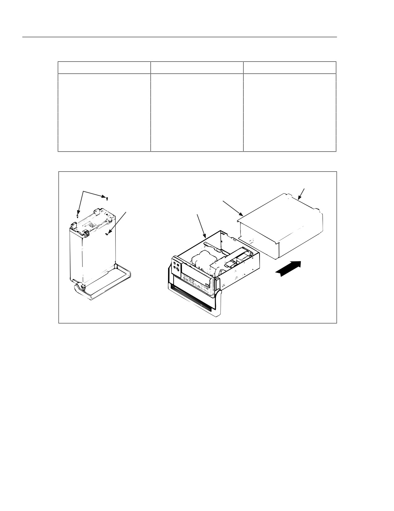
Figure 8-1. Disassembly
8-6
Option -05 IEEE-488 Interface
Theory of Operation
8
qb41c.epc
Figure 8-2. IEEE-488 Interface Connector
8-7
45
Service Manual
qb42c.eps
Figure 8-3. IEEE-488 Module Assembly
8-10. General Maintenance
8-11. Removing the IEEE-488 Interface Option
The following instructions can be used for access and servicing an IEEE-488 Interface
Option that is already installed in a Fluke 45 Dual Display Multimeter. For initial
installation, refer to the Instruction Sheet (PN 856005) provided with the option.
1. Make sure the meter is turned off and unplugged from the power outlet.
2. Remove the screw on the bottom of the meter case and the two screws from the rear
bezel (as shown in Figure 8-1A). While holding the front panel, slide the case and
rear bezel off the chassis (see Figure 8-1B). (At this point, the rear bezel is not
secured to the case.)
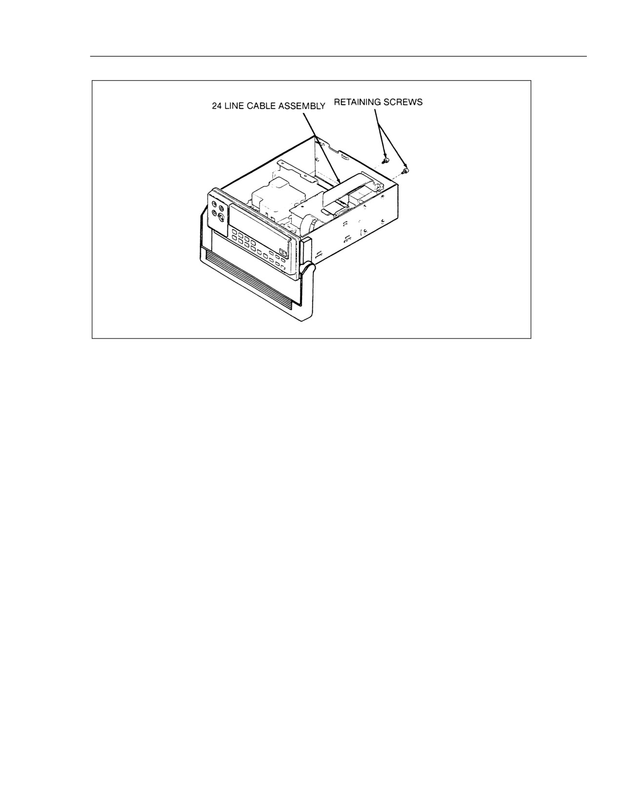
3. Using needle nose pliers, disconnect the 24-line cable assembly at the IEEE-488
PCA by alternately pulling up on each end of its connector. See Figure 8-2.
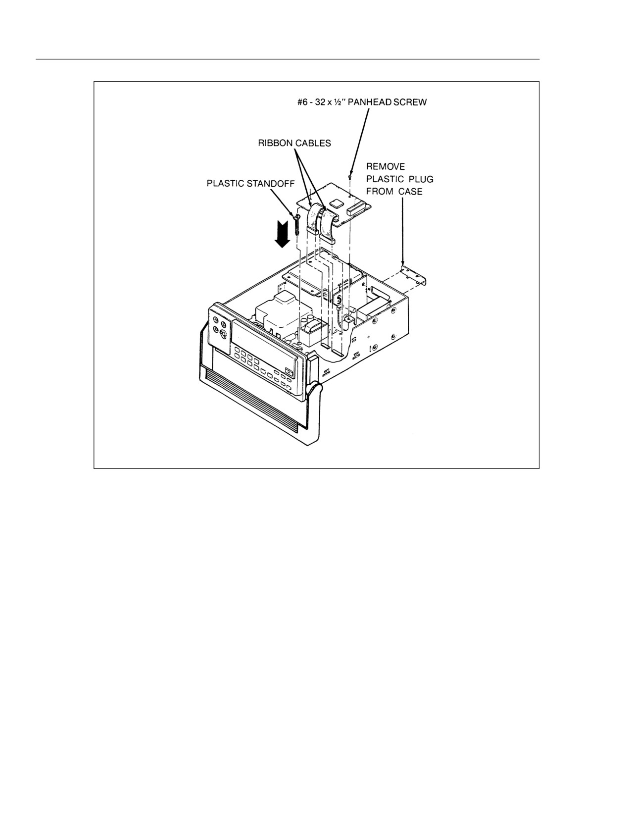
4. Refer to Figure 8-3 for the remaining steps. Remove the panhead Phillips screw at
the rear of the IEEE-488 PCA.
8-8
Option -05 IEEE-488 Interface
Performance Testing
8
5. Using needle nose pliers, detach the two ribbon cables at the front part of the IEEE-
488 PCA. Alternately pull up on each end of the cable connectors.
6. Remove the IEEE-488 PCA, disengaging the assembly from both the small slot in
the side of the meter and the plastic standoff at the front corner of the assembly.
8-12.
Installing the IEEE-488 Interface Option
Use the following procedure to install the IEEE-488 Interface Option.
1. Turn the meter off, and unplug the power connection.
2. Check that the plastic standoff remains in the appropriate hole in the meter PCA
(narrow end of the standoff down; see Figure 8-3).
3. If necessary, install the two ribbon cables on the IEEE-488 PCA. Each cable fits in
only one socket and in only one direction. Make sure the cables lock firmly in place.
4. Attach opposite ends of the ribbon cables onto the Fluke 45 Main PCA.
5. Install the IEEE-488 PCA in the Fluke 45 with the dual ribbon cables facing the
front of the meter. The IEEE-488 PCA slips into the small slot in the side of the
meter. The end of the plastic standoff fits into the hole in the IEEE-488 PCA. Make
sure the IEEE-488 PCA is firmly gripped against the retainer on the standoff. The
rear of the IEEE-488 PCA should rest upon the support just forward of the
transformer.
6. Secure the rear of the IEEE-488 PCA with the panhead Phillips screw.
7. Connect the 24-line cable assembly to the IEEE-488 PCA. (See Figure 8-2.)
8. Reinstall the meter case so it seats properly in the front panel. Attach the rear bezel
with the two panhead Phillips screws, and secure the case with the flathead Phillips
screw in the bottom.
8-13. Performance Testing
Use the performance test program in Figure 8-1 to verify operation of the IEEE-488
Interface. This program is written for use with the Fluke 182A Instrument Controller and
its interpreted BASIC language. The program may be adapted to the language of any
IEEE-488 controller.
This performance test communicates to a meter that has been configured for IEEE-488
operation at address 0. Lines 160 and 170 initialize the IEEE-488 bus and send a
selective device clear to the meter. A multiple byte command is sent to the meter (by line
190) to clear the meter status. Another command sequence (including a query) is sent to
the meter by line 210; the meter asserts Service Request (SRQ) to signal that a response
is available. Lines 530 through 560 first poll the meter for status, then input the response
from the meter. Lines 230 through 270 test for proper operation and print the results.
8-9
45
Service Manual
140 IA% = 0%
! instrument IEEE address
150 S% = -1%
! initialize spl response
160 TERM
! terminate input only on EOI
170 INIT PORT 0
! initialize IEEE-488 bus
180 CLEAR @IA%
! selective device clear
190 PRINT @IA%,"*cls"
! clear instrument status
200 ON SRQ GOTO 530
! enable SRQ interrupt
210 PRINT @IA%,"*cls;*sre 16;*idn?"
! SRQ on Message Available
220 WAIT 500% FOR SRQ
! allow time to execute commands
230 IF S% >= 0% THEN 260
240
PRINT "Instrument failed to generate a Service Request"
250
STOP
260 PRINT "Serial Poll =";S%;"(should be 80)."
270 PRINT "Identification Query Response = ";R$
280 STOP
500 !
510 ! Service Request interrupt
520 !
530 S% = SPL(IA%)
! get instrument serial poll status
540 IF S% AND 16% THEN 550 ELSE 560
550
INPUT LINE @IA%,R$
! if MAV set get the response
560 RESUME 230
! end of SRQ interrupt
999 END
Figure 8-4. IEEE-488 Interface Performance Test
8-14. Troubleshooting
8-15. Power-up Problems
The following discussion identifies probable fault areas if the installation of an IEEE-
488 Interface Option causes power-up failure for the Fluke 45. The problem is probably
a short on A5P2 or A5P3; the Microprocessor on the Main Assembly is prevented from
accessing ROM and RAM correctly. Two extender cables are available (PN 867952 and
867957) to assist during troubleshooting.
• The first thing to check is whether GND is shorted to either VCC or VCC2 on the
IEEE Assembly.
• The short may also be an interface signal to either VCC, GND, or another interface
signal. The logical signals to check are DATA(7..0), ADD(15..0), RD*, WR*, E, and
RESET*.
• The short may be due to a CMOS input that has been damaged from static discharge;
the short is then detectable only when the circuit is powered up. Use an oscilloscope
to check activity on each of the interface signals. Verify that signals are able to
transition normally between 0 and 5V.
8-16. Communication Problems
8-17. Failure to Select IEEE-488 Interface Option
IEEE-488 Interface selection procedures are described in Chapter 3.
8-10
Option -05 IEEE-488 Interface
Troubleshooting
8
If the IEEE-488 Interface Option is not detected by Fluke 45 software, there may be a
problem with the OPS or ACON* signal. The IEEE Interface Option grounds the OPS
signal (A5P2-18), which is normally pulled up to VCC on the Fluke 45 Main Assembly.
The Microprocessor determines that the IEEE-488 Interface Option is not installed if
OPS (A1U6-29) is detected high.
Further, software does not allow the IEEE-488 Interface Option to be selected if the
ACON* signal is detected high. Since ACON* is high when the meter is operating on
battery power, the IEEE-488 Interface Option cannot be selected as the active interface
during battery operation. The displayed "IEEE" message is dim, and the battery indicator
blinks if the Fluke 45 software detects ACON* to be high when the option editor is
entered. The ACON* signal (A1U6-33) is low when the meter is operating from line
power.
8-18.
Failure to Handshake on IEEE-488 Bus
Check VCC2 with a voltmeter. When the Fluke 45 is operating on line power, VCC2
should be about 0.1V lower than VCC. VCC2 is controlled by the Microprocessor,
which sets A1U6-28 high when operating on line power and causes OPTSW* to be
driven to a -5.0V dc level. The OPTSW* signal controls the gate of FET switch A5Q1
on the IEEE-488 Interface Option to turn VCC2 on.
The Reset circuit consists of A5CR1, A5R1, A5U2, and A5U9. When the meter is
operating on batteries, the Reset circuit converts the OPTSW* signal to a digital signal
that disables access to A5U6. When operating from batteries, OPTSW* is at about 5.0V
dc, A5U2-9 is high, A5U2-10 is low, and A5U9-9 is low to reset A5U6 via pin 22.
When the meter is connected to ac line voltage again, this circuit resets A5U6. OPTSW*
transitions to -5.0V dc, A5U2-9 is low (near GND), A5U2-10 is high, and A5U9-9 stays
low until the Address Decoder detects a memory access to the IEEE-488 Interface
Option. About 1.0 ms after OPTSW* goes to -5.0V dc, the initial read access clocks
A5U9-11, causing A5U9-9 to go high to remove the reset from A5U6-22. This action is
followed by another "dummy" read cycle for delay. The Main Assembly then sends six
write cycles to initialize A5U6. The IRQ2 interrupt is then enabled, and the serial poll
status byte is initialized. At this point, the IEEE-488 Interface Option is ready to respond
to transactions on the IEEE-488 bus.
Note
Each time that the IEEE Interface Option is selected in the BAUD menu
(by pressing [AUTO]), the IEEE-488 Interface Option initialization is
repeated as described above, with the exception that no hardware reset is
performed via the OPTSW* signal.
8-19.
Failure to Enter Remote
If the IEEE-488 Interface Option does not enter remote, check that the remote/local
control circuit is operating properly. When the IEEE-488 Interface Option is the active
instrument interface, the remote/local control state is polled by the Main PCA
approximately every 1.0 ms. Normally, A5U5-8 goes low for approximately 1.0 µs
during the read cycle that checks the state of A5U6. If A5U3-11 is low during the read
cycle, A5U6 is in the local state. If A5U3-11 is high during the read cycle, A5U6 is in
the remote state. When A5U6 indicates that it is in remote, the REMOTE indicator on
the display is turned on.
8-11
45
Service Manual
8-20.
Failure to Receive Multiple Character Commands
Monitor the interrupt signal from A5U6-10 during attempts to communicate with the
meter. Each byte received with the ATN signal (A5U6-31) high should cause the
interrupt signal to go low. Follow the interrupt signal through A5U4, and verify that it
arrives at A5J3 properly. If the interrupt is not detected by A1U6, it will remain low
indefinitely. A5U6-10 will only go high when both the interrupt is detected and the
received byte is removed from A5U6 by A1U6.
8-21.
Failure to Transmit Query Responses
Check that TE (A5U6-24) goes high when the interface is addressed to talk. This signal
must go high to allow the bus interface transceivers to change the direction of DIO1
through DIO8, EOI, DAV, NRFD, and NDAC. Verify that each of these signals passes
through A5U7 and A5U8 properly.
8-22.
Failure to Generate an End or Identify (EOI)
When the IEEE-488 Interface Option sends the Line Feed termination character with a
message, the EOI signal should also be set true. When EOI is true, A5U6-30 should go
low. Follow this signal from A5J1 through A5U8 to A5U6.
8-23.
Failure to Generate a Service Request (SRQ)
When a Service Request is being generated, A5U6-32 should be low. Follow this signal
through A5U8 to connector A5J1. When a Serial Poll (SPL) is performed by the IEEE-
488 bus controller, A5U6-32 will go high again.
Note
If the meter is in the remote state without front panel lockout (i.e., REMS),
a service request can be sent from the front panel by pressing [UPB].
8-24. Schematic Diagram
The schematic diagram for the IEEE-488 Interface Option is included in Chapter 9 of
this manual.
8-25. List of Replaceable Parts
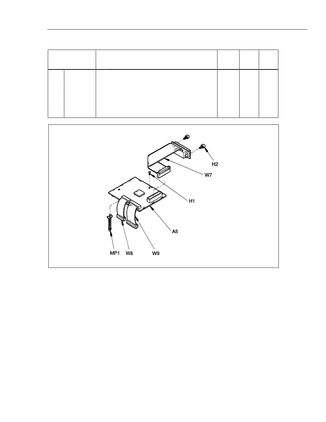
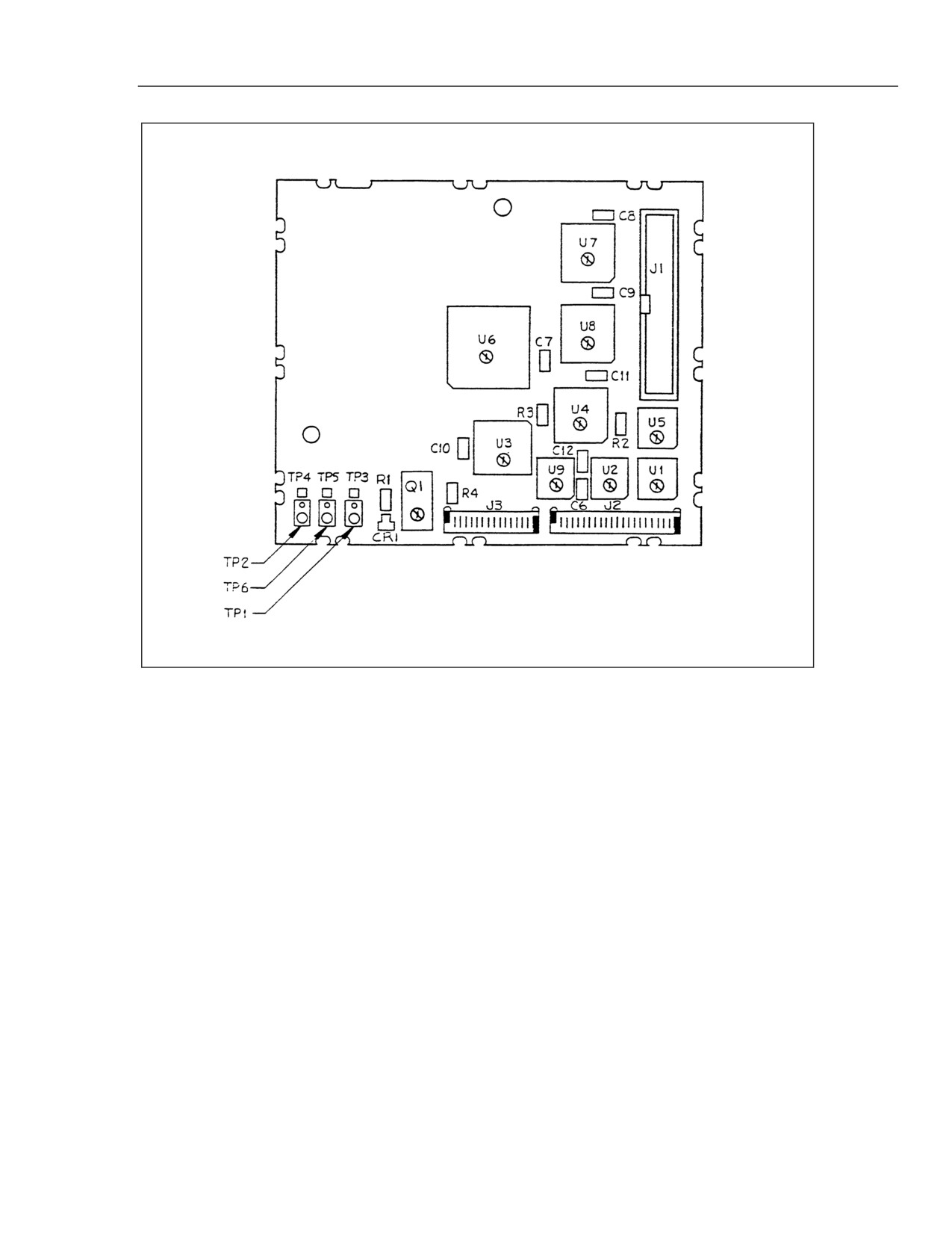
Figures 8-4 and 8-5 provide illustration for the parts lists in Tables 8-3 and 8-4,
respectively. Refer to Chapter 6 for parts ordering information.
8-12
Option -05 IEEE-488 Interface
List of Replaceable Parts
8
Table 8-2. Option -05 IEEE-488 Interface Final Assembly
Reference
Fluke
Total
Description
Note
Designator
Stock
Qty.
No.
A
5
IEEE-488 INTERFACE PCA
814152
1
H
1
SCREW,PH,P,LOCK,STL,6-32,.250
152140
1
H
2
CONN ACC,MICRO-RIBBON,SCREW LOCK KIT
836585
1
MP
1
SPACER,SNAP,PWB,NYL,1.375
845347
1
TM
1
PRINT MATL,INST SHT,FLUKE 45/IEEE-488
856005
1
W
7
CABLE ASSY,IEEE
834978
1
W
8
CABLE ASSY,FLAT,14 COND,MICROMOD,3 IN
831560
1
W
9
CABLE ASSY,FLAT,20 COND,MICROMOD,3 IN
831578
1
45-5 T&B
qb43c.eps
Figure 8-5. Option -05 IEEE-488 Interface Final Assembly
8-13

45
Service Manual
Table 8-3. A5 IEEE-488 Interface PCA
Fluke
Reference
Total
Description
Stock
Note
Designator
Qty.
No.
C
6- 11
CAP,CER,0.1UF,±10%,25V,X7R,1206
747287
6
C
12
CAP,CER,0.022UF,±10%,50V,X7R,1206
747279
1
CR
1
DIODE,SI,BV=75V,IO=250MA,SOT23
830489
1
J
1
HEADER,2 ROW,.100CTR,24 PIN
831834
1
J
2
HEADER,1 ROW,.050CTR,20 PIN
831529
1
J
3
HEADER,1 ROW,.050CTR,14 PIN
831511
1
Q
1
TRANSISTOR,SI,PMOS,1W,D-PAK
836544
1
R
1,3
RES,CERM,5.1K,±5%,125W,200PPM,1206
746560
2
R
2
RES,CERM,47K,±5%,.125W,200PPM,1206
746685
1
R
4
RES,CERM,220,±5%,.125W,200PPM,1206
746347
1
U
1,2
IC,CMOS,QUAD INPUT NOR GATE,SOIC
830711
2
U
3
IC,CMOS,OCTAL BUS TRANSCEIVER,SOIC
742577
1
U
4
IC,CMOS,OCTL LINE DRVR,SOIC
801043
1
U
5
IC,CMOS,8 INPUT NAND GATE,SOIC
830729
1
U
6
IC,NMOS,GPIB CONTROLLER,PLCC
887190
1
U
7
IC,LSTTL,OCTAL GPIB XCVR,SOIC
831651
1
U
8
IC,LSTTL,OCTAL GPIB XCVR,SOIC
831669
1
U
9
*
IC,CMOS,DUAL D F/F,+EDG TRG,SOIC
782995
1
8-14
Option -05 IEEE-488 Interface
List of Replaceable Parts
8
qb44c.eps
Figure 8-6. A5 IEEE-488 Interface PCA
8-15
Chapter 9
Schematic Diagrams
Figure
Title
Page
9-1
A1 Main PCA
9-2
9-2
A2 Display PCA
9-8
9-3
A1A1 True Rms PCA
9-10
9-4
A4 Battery PCA
9-12
9-5
A5 IEEE-488 Interface PCA
9-14
9-1
45
Service Manual
45-4001
qb30f.eps
Figure 9-1. A1 Main PCA
9-2