FLUKE 45 Dual Display Multimeter. Service Manual (For IEC 1010 Meters Only) - page 1
®
45
Dual Display Multimeter
Service Manual
For IEC 1010 Meters Only
PN 609203
March 1999 Rev.1, 1/04
LIMITED WARRANTY & LIMITATION OF LIABILITY
Each Fluke product is warranted to be free from defects in material and workmanship under
normal use and service. The warranty period is one year and begins on the date of shipment.
Parts, product repairs and services are warranted for 90 days. This warranty extends only to the
original buyer or end-user customer of a Fluke authorized reseller, and does not apply to fuses,
disposable batteries or to any product which, in Fluke’s opinion, has been misused, altered,
neglected or damaged by accident or abnormal conditions of operation or handling. Fluke
warrants that software will operate substantially in accordance with its functional specifications for
90 days and that it has been properly recorded on non-defective media. Fluke does not warrant
that software will be error free or operate without interruption.
Fluke authorized resellers shall extend this warranty on new and unused products to end-user
customers only but have no authority to extend a greater or different warranty on behalf of Fluke.
Warranty support is available if product is purchased through a Fluke authorized sales outlet or
Buyer has paid the applicable international price. Fluke reserves the right to invoice Buyer for
importation costs of repair/replacement parts when product purchased in one country is submitted
for repair in another country.
Fluke’s warranty obligation is limited, at Fluke’s option, to refund of the purchase price, free of
charge repair, or replacement of a defective product which is returned to a Fluke authorized
service center within the warranty period.
To obtain warranty service, contact your nearest Fluke authorized service center or send the
product, with a description of the difficulty, postage and insurance prepaid (FOB Destination), to
the nearest Fluke authorized service center. Fluke assumes no risk for damage in transit.
Following warranty repair, the product will be returned to Buyer, transportation prepaid (FOB
Destination). If Fluke determines that the failure was caused by misuse, alteration, accident or
abnormal condition of operation or handling, Fluke will provide an estimate of repair costs and
obtain authorization before commencing the work. Following repair, the product will be returned to
the Buyer transportation prepaid and the Buyer will be billed for the repair and return
transportation charges (FOB Shipping Point).
THIS WARRANTY IS BUYER’S SOLE AND EXCLUSIVE REMEDY AND IS IN LIEU OF ALL OTHER
WARRANTIES, EXPRESS OR IMPLIED, INCLUDING BUT NOT LIMITED TO ANY IMPLIED WARRANTY
OF MERCHANTABILITY OR FITNESS FOR A PARTICULAR PURPOSE. FLUKE SHALL NOT BE LIABLE
FOR ANY SPECIAL, INDIRECT, INCIDENTAL OR CONSEQUENTIAL DAMAGES OR LOSSES,
INCLUDING LOSS OF DATA, WHETHER ARISING FROM BREACH OF WARRANTY OR BASED ON
CONTRACT, TORT, RELIANCE OR ANY OTHER THEORY.
Since some countries or states do not allow limitation of the term of an implied warranty, or
exclusion or limitation of incidental or consequential damages, the limitations and exclusions of
this warranty may not apply to every buyer. If any provision of this Warranty is held invalid or
unenforceable by a court of competent jurisdiction, such holding will not affect the validity or
enforceability of any other provision.
To locate an authorized service center, visit us on the World Wide Web: www.fluke.com
or call Fluke using the phone numbers listed below:
USA and Canada: 1-888-99-FLUKE (1-888-993-5853)
Europe: +31 402-675-200
Japan: +81-3-3434-0181
Singapore: +65-738-5655
Anywhere in the world: +1-425-446-5500
Fluke Corporation
Fluke Europe B.V.
P.O. Box 9090
P.O. Box 1186
Everett, WA 98206-9090
5602 BD Eindhoven
U.S.A.
The Netherlands
5/94
Table of Contents
Chapter
Title
Page
1
Introduction and Specifications
1-1
1-1.
Introduction
1-3
1-2.
Operating Instructions
1-3
1-3.
Options and Accessories
1-3
1-4.
Organization of the Service Manual
1-4
1-5.
Conventions
1-5
1-6.
Specifications
1-6
2
Theory of Operation
2-1
2-1.
Introduction
2-3
2-2.
Functional Block Description
2-3
2-3.
Power Supply
2-3
2-4.
Analog Measurement Processor
2-3
2-5.
Input Protection Circuit
2-3
2-6.
Input Signal Conditioning
2-3
2-7.
Analog-to-Digital (A/D) Converter
2-3
2-8.
Serial Communication (Guard Crossing)
2-3
2-9.
Digital Kernel
2-5
2-10.
Display Assembly
2-5
2-11.
IEEE-488 Interface Option (-05)
2-5
2-12.
Battery Pack Option (-01)
2-5
2-13.
Detailed Circuit Description
2-5
2-14.
Power Supply Circuit Description
2-5
2-15.
Raw DC Supply
2-6
2-16.
5-Volt Switching Supply
2-6
2-17.
Inverter
2-7
2-18.
Analog Measurement Processor
2-7
2-19.
Input Protection
2-10
2-20.
Input Signal Conditioning
2-10
2-21.
Relays
2-11
2-22.
DC Volts
2-12
2-23.
Ohms
2-12
2-24.
100 MΩ and 300 MΩ Ranges
2-14
2-25.
AC Volts
2-14
i
45
Service Manual
2-26.
DCmA
2-15
2-27.
ACmA
2-15
2-28.
Amps
2-15
2-29.
Diode/Continuity Test
2-15
2-30.
Frequency
2-15
2-31.
Active Filter
2-16
2-32.
A/D Converter
2-17
2-33.
Serial Communication (Guard Crossing)
2-18
2-34.
Digital Kernel
2-18
2-35.
RS-232 Interface
2-19
2-36.
Microprocessor
2-19
2-37.
EEROM
2-19
2-38.
RAM
2-20
2-39.
ROM
2-20
2-40.
IEEE-488 Option Connections
2-20
2-41.
Display Assembly
2-20
2-42.
Main Assembly Connector
2-20
2-43.
Front Panel Switches
2-20
2-44.
Display
2-21
2-45.
Beeper Drive Circuit
2-21
2-46.
Watchdog Timer and Reset Circuit
2-21
2-47.
Display Controller with FIP
2-22
3
General Maintenance
3-1
3-1.
Introduction
3-3
3-2.
Warranty Repairs and Shipping Information
3-3
3-3.
General Maintenance Information
3-3
3-4.
Required Equipment
3-3
3-5.
Power Requirements
3-3
3-6.
Static Safe Handling
3-3
3-7.
Cleaning
3-4
3-8.
Fuse Test and Replacement
3-4
3-9.
Line Fuse
3-4
3-10.
Current Input Fuses
3-4
3-11.
Testing Current Input Fuses
3-4
3-12.
Replacing the 500 mA and 440 mA Input Fuses (F1 and F5)
3-5
3-13.
Replacing the 10 A Input Jack Fuse (F2)
3-6
3-14.
Disassembly Procedures
3-7
3-15.
Remove the Meter Case
3-7
3-16.
Remove Handle and Mounting Brackets
3-7
3-17.
Remove the Front Panel Assembly
3-8
3-18.
Remove the Display PCA
3-8
3-19.
Remove the IEEE-488 Option
3-9
3-20.
Remove the Main PCA
3-9
3-21.
Remove the Analog Measurement Processor Shields
3-9
3-22.
Remove the Rms PCA
3-10
3-23.
Remove the Battery Option
3-10
3-24.
Disconnect Miscellaneous Chassis Components
3-10
3-25.
Assembly Procedures
3-10
3-26.
Install Miscellaneous Chassis Components
3-10
3-27.
Install the Battery Option
3-11
3-28.
Install the Rms PCA
3-11
3-29.
Install the Analog Measurement Processor Shields
3-11
3-30.
Install the Main PCA
3-11
ii
Contents (continued)
3-31.
Install the IEEE-488 Option
3-12
3-32.
Assemble the Front Panel Assembly
3-12
3-33.
Install the Front Panel Assembly
3-15
3-34.
Install the Handle and Mounting Brackets
3-15
3-35.
Install the Meter Case
3-15
4
Performance Testing and Calibration
4-1
4-1.
Introduction
4-3
4-2.
Required Equipment
4-3
4-3.
Performance Tests
4-4
4-4.
Front Panel Calibration
4-7
4-5.
Introduction
4-7
4-6.
Entering Calibration Mode
4-8
4-7.
Exiting Calibration Mode
4-9
4-8.
DC Volts Calibration (Front Panel)
4-9
4-9.
AC Volts Calibration (Front Panel)
4-9
4-10.
DC and AC Milliamp Calibration (Front Panel)
4-9
4-11.
DC and AC Amps Calibration (Front Panel)
4-11
4-12.
Ohms Calibration (Front Panel)
4-11
4-13.
Alternate Ohms Calibration (Front Panel)
4-13
4-14.
Continuity/Hysteresis Threshold Calibration (Front Panel)
4-13
4-15.
Frequency Calibration (Front Panel)
4-13
4-16.
C2 Adjustment Procedure
4-13
4-17.
Editing the Prompt for Different Calibration Points
4-14
4-18.
Calibration Using the Computer Interface
4-15
4-19.
Setup
4-15
4-20.
RS-232 Interface
4-15
4-21.
IEEE-488 Interface
4-16
4-22.
The Calibration Procedure
4-18
4-23.
DC Volts Calibration (Computer Interface)
4-19
4-24.
AC Volts Calibration (Computer Interface)
4-19
4-25.
DC and AC Milliamps Calibration (Computer Interface)
4-19
4-26.
DC and AC Amps Calibration (Computer Interface)
4-19
4-27.
Ohms Calibration (Computer Interface)
4-19
4-28.
Continuity/Hysteresis Threshold Calibration (Computer Interface)
4-20
4-29.
Frequency Calibration (Computer Interface)
4-20
4-30.
Concluding Calibration Using the Computer Interface
4-20
4-31.
Alternate Ohms Calibration (Computer Interface)
4-20
5
Diagnostic Testing and Troubleshooting
5-1
5-1.
Introduction
5-3
5-2.
Servicing Surface-Mount Assemblies
5-3
5-3.
Error Codes
5-4
5-4.
General Troubleshooting Procedures
5-10
5-5.
Power Supply Troubleshooting
5-10
5-6.
Raw DC Supply
5-10
5-7.
5-Volt Switching Supply
5-11
5-8.
Inverter
5-12
5-9.
Analog Troubleshooting
5-13
5-10.
Uart Test
5-13
5-11.
DC Volts Troubleshooting
5-14
5-12.
AC Volts Troubleshooting
5-14
5-13.
Ohms Troubleshooting
5-14
5-14. Digital Troubleshooting
5-15
iii
45
Service Manual
5-15. Display Assembly Troubleshooting
5-17
5-16. Calibration Failures
5-19
5-17.
Introduction
5-19
5-18.
Calibration-Related Components
5-20
5-19.
Calibration Interrelationships
5-21
5-20.
Retrieving Calibration Constants
5-21
5-21.
Replacing the EEROM A1U5
5-21
6
List of Replaceable Parts
6-1
6-1.
Introduction
6-3
6-2.
How to Obtain Parts
6-3
6-3.
How to Contact Fluke
6-4
6-4.
Manual Status Information
6-4
6-5.
Newer Instruments
6-4
6-6.
Parts
6-4
7
Option -01 Battery Pack
7-1
7-1.
Introduction
7-3
7-2.
Specifications
7-3
7-3.
Theory of Operation
7-3
7-4.
Functional Block Description
7-3
7-5.
Switching Power Supply
7-5
7-6.
Cycle/Float Charge Rate Switch
7-5
7-7.
Low Battery Indicator Detector
7-5
7-8.
Low Battery Disconnect
7-5
7-9.
Constant Voltage Trickle Charger
7-6
7-10.
Other Circuits
7-6
7-11. General Maintenance
7-6
7-12.
Removal
7-6
7-13.
Installation
7-7
7-14. Performance Testing
7-9
7-15.
General Operability
7-9
7-16.
Low Battery Indicator Detector and Low Battery Disconnect Test.
7-10
7-17.
Cycle/Float Charge Rate Switch Test
7-10
7-18. Calibration
7-12
7-19. Troubleshooting
7-13
7-20. Additional Tests
7-14
7-21. Schematic Diagram
7-14
7-22. List of Replaceable Parts
7-14
8
Option -05 IEEE-488 Interface
8-1
8-1.
Introduction
8-3
8-2.
Theory of Operation
8-3
8-3.
Functional Block Description
8-3
8-4.
Detailed Circuit Description
8-3
8-5.
Main Assembly Connectors
8-3
8-6.
Address Decoding Circuit
8-3
8-7.
Isolation Circuits
8-4
8-8.
IEEE-488 Controller
8-4
8-9.
IEEE-488 Transceivers/Connector
8-5
8-10. General Maintenance
8-8
8-11.
Removing the IEEE-488 Interface Option
8-8
8-12.
Installing the IEEE-488 Interface Option
8-9
iv
Contents (continued)
8-13. Performance Testing
8-9
8-14. Troubleshooting
8-10
8-15.
Power-up Problems
8-10
8-16.
Communication Problems
8-10
8-17.
Failure to Select IEEE-488 Interface Option
8-10
8-18.
Failure to Handshake on IEEE-488 Bus
8-11
8-19.
Failure to Enter Remote
8-11
8-20.
Failure to Receive Multiple Character Commands
8-12
8-21.
Failure to Transmit Query Responses
8-12
8-22.
Failure to Generate an End or Identify (EOI)
8-12
8-23.
Failure to Generate a Service Request (SRQ)
8-12
8-24. Schematic Diagram
8-12
8-25. List of Replaceable Parts
8-12
9
Schematic Diagrams
9-1
Index
v
List of Tables
Table
Title
Page
1-1.
Accessories
1-4
2-1.
Analog Measurement Processor Pin Name Description
2-9
2-2.
Relay Operation
2-11
2-3.
Reference Resistance
2-13
2-4.
AC Volts Input Signal Dividers
2-14
2-5.
Front Panel Switch Scanning
2-21
2-6.
Display Initialization Modes
2-23
3-1.
Fuses
3-6
4-1.
Recommended Test Equipment
4-3
4-2.
Performance Tests for Volts, Diode Test, Ohms, and Frequency Functions
4-5
4-3.
Performance Tests for mA Current Functions
4-7
4-4.
Performance Tests for Current Functions
4-7
4-5.
Front Panel Calibration
4-10
4-6.
Specifications Increase with Different Calibration Points
4-15
4-7.
Calibration Using the Computer Interface
4-17
4-8.
Calibration Mode Computer Interface Commands
4-21
4-9.
EEROM Calibration Constants
4-22
5-1.
Error Codes
5-5
5-2.
Power Supplies
5-11
5-3.
DC Volts Troubleshooting
5-14
5-4.
AC Volts Troubleshooting
5-15
5-5.
Display Initialization
5-18
5-6.
Calibration Steps and Related Components
5-22
5-7.
Components Unique to Calibration Steps
5-23
5-8.
Calibration Hierarchy
5-24
5-9.
Calibration Constants
5-24
6-1.
Manual Status Information
6-4
6-2.
Final Assembly
6-5
6-3.
A1 Main PCA
6-8
6-4.
A1A1 True Rms PCA
6-12
6-5.
A2 Display PCA
6-13
7-1.
Option -01 Battery Pack Final Assembly
7-15
7-2.
A4 Battery Pack PCA
7-16
8-1.
IEEE-488 Transceiver Control
8-6
8-2.
Option -05 IEEE - 488 Interface Final Assembly
8-13
vii
List of Figures
Figure
Title
Page
2-1.
Overall Functional Block Diagram
2-4
2-2.
Analog Simplified Schematic Diagram
2-8
2-3.
DC Volts 300 V Range Simplified Schematic
2-12
2-4.
Ohms Simplified Schematic
2-13
2-5.
AC Buffer Simplified Schematic
2-14
2-6.
DC mA and Amps Simplified Schematic
2-16
2-7.
Active Filter Simplified Schematic
2-17
2-8.
A/D Converter Simplified Schematic
2-18
2-9.
Command Byte Transfer Waveforms
2-23
2-10.
Grid Control Signal Timing
2-24
2-11.
Grid-Anode Timing Relationships
2-24
3-1.
Replacing the Line Fuse (F3)
3-5
3-2.
Replacing the External 100 mA Input Fuse (F1)
3-6
3-3.
Removing the Case
3-7
3-4.
Removing the Handle and Handle Mounting Brackets
3-8
3-5.
Assembly Details
3-13
4-1.
Four Wire Configuration
4-12
4-2.
C2 Location
4-14
5-1.
Test Point Locator
5-6
5-2.
Volt Switching Supply
5-12
5-3.
Main Processor Timing
5-16
5-4.
Display Controller to Microprocessor Signals
5-17
5-5.
Primary Display
5-18
5-6.
Secondary Display
5-18
6-1.
Final Assembly
6-6
6-2.
A1 Main PCA
6-11
6-3.
A1A1 True Rms PCA
6-12
6-4.
A2 Display PCA
6-14
7-1.
Battery Pack Option Functional Block Diagram
7-4
7-2.
Removing the Case
7-7
7-3.
Installing the Battery Kit
7-8
7-4.
Battery Pack Option Connecting Cable
7-9
7-5.
Cycle/Float Charge Rate Switch Test
7-11
7-6.
Unplugging the Battery Pack Connectors
7-13
7-7.
Test Points and Adjustments
7-14
ix
45
Service Manual
7-8. Option-01 Battery Pack Final Assembly
7-15
7-9. A4 Battery Pack PCA
7-18
8-1. Disassembly
8-6
8-2. IEEE-488 Interface Connector
8-7
8-3. IEEE-488 Module Assembly
8-8
8-4. IEEE-488 Interface Performance Test
8-10
8-5. Option -05 IEEE-488 Interface Final Assembly
8-13
8-6. A5 IEEE-488 Interface PCA
8-15
9-1. A1 Main PCA
9-2
9-1. A1 Main PCA
9-2
9-2. A2 Display PCA
9-8
9-3. A1A1 True Rms PCA
9-10
9-4. A4 Battery PCA
9-12
9-5. A5 IEEE-488 Interface PCA
9-14
x
Chapter 1
Introduction and Specifications
Title
Page
1-1.
Introduction
1-3
1-2.
Operating Instructions
1-3
1-3.
Options and Accessories
1-3
1-4.
Organization of the Service Manual
1-4
1-5.
Conventions
1-5
1-6.
Specifications
1-6
1-1
Introduction and Specifications
Introduction
1
1-1.
Introduction
The Fluke 45 Dual Display Multimeter (also referred to as "the meter") is a 4-1/2-digit
(30,000-count) meter with a 5-digit (100,000-count) high resolution mode designed for
bench-top, field service, and system applications. The meter uses a dual vacuum-
fluorescent display, allowing for two types of readings from a single input. Primary and
secondary displays show the user-defined readings side by side. Even though the
readings are made sequentially, the displays show both readings at all times for ease of
comparison.
Some features provided by the meter are:
• Computer interface operation via the RS-232 interface (included) or the IEEE-488
interface (optional). The meter is fully programmable for use on the IEEE Standard
488.1 (1987). The meter is also designed in compliance with supplemental standard
IEEE-488.2 (1987).
• True rms ac
•
(AC + DC) rms, calculated
• Frequency measurements to greater than 1 MHz.
•
1 µV sensitivity in volts dc
• Decibels with variable reference impedance and audio power measurement
capability.
• A compare mode to determine if a measurement is within, above, or below a
designated range.
•
100,000, 30,000, and 3,000 selectable count resolution, with reading speeds of 2.5, 5,
and 20 readings per second (rps), respectively.
• Built-in self-tests with closed-case calibration (no internal adjustments).
1-2.
Operating Instructions
Full operating instructions are provided in the Fluke 45 Users Manual. Reference to
these instructions may be necessary during some of the maintenance and repair
procedures presented in this Service Manual. For quick references, an operating
instruction summary is presented on the inside of the front cover of the Service Manual.
For more detailed information, refer to the Users Manual.
1-3.
Options and Accessories
Three options are available. These options can be installed either at the factory or in the
field. The following discussions pertain to the field-installable option kits:
• The Battery Kit (Option -01K) consists of a rechargeable, 8 V, lead-acid battery,
with battery bracket and charger assembly. The battery has a typical operating time
of eight hours and is fully operable at ambient temperatures between 0 and 50ºC.
• The IEEE-488 Interface Kit (Option -05K) consists of a printed circuit assembly,
connecting cables, and mounting hardware. This option provides full
programmability, external trigger input, and automated calibration. The IEEE-488
computer interface command set is identical to the RS-232 interface commands
wherever possible.
• Option -15K combines Options -01K and -05K as a single kit.
1-3
45
Service Manual
The Fluke 45 Dual Display Multimeter can be mounted in a standard 19-inch rack panel
on either the right-hand or left-hand side using the Fluke M00-200-634 Rack Mount Kit.
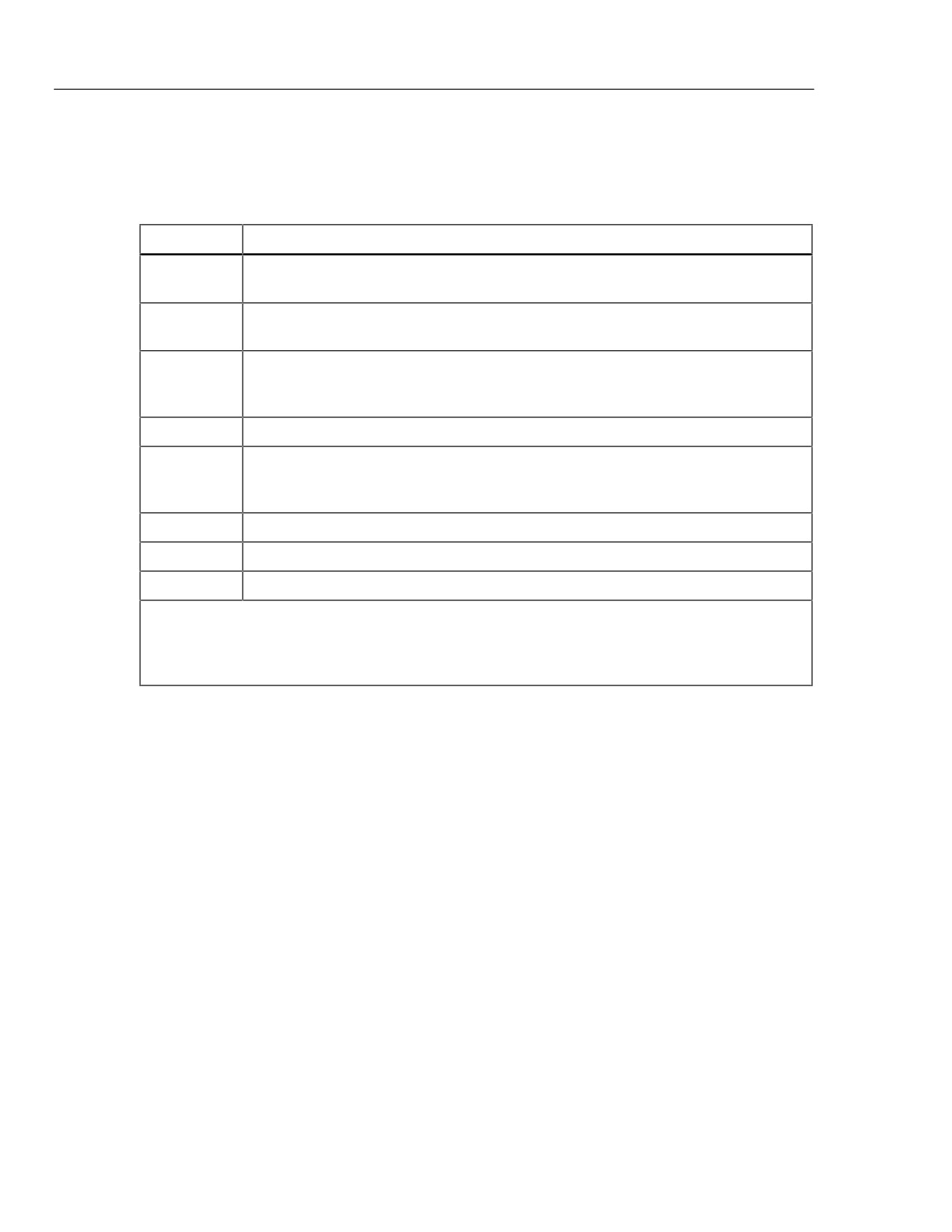
Accessories for the Fluke 45 are listed in Table 1-1.
Table 1-1. Accessories
Model
Description
C40
Soft carrying case. Provides padded protection for the meter. Includes a pocket for the
manual and pouch for the test leads and line cord.
M00-200-
Rackmount Kit. Allows meter to be mounted on either the right or left side of a standard
634
19-inch rack.
RS40
RS-232 terminal interface cable. Connects other Fluke 45 to any terminal or printer with
properly configured DTE connector (DB-25, female pins), including an IBM PC®, IBM
PC/XT® or IBM PS/2 (models 25, 30, 50, P60, 70, and 80).
RS41
RS-232 modem cable. Connects the Fluke 45 to a modem.
S45
QuickStart™, a PC software package, simplifies operation of the Fluke 45 when using
the RS-232 computer interface. Readings are recorded in files that can be accessed by
Lotus 1-2-3®, dBase III® and other graphics packages.
Y8021
Shielded IEEE-488 one-meter (39.4 inches) cable, with plug and jack at each end.
Y8022
Shielded IEEE-488 two-meter (78.8 inches) cable, with plug and jack at each end.
Y8023
Shielded IEEE-488 four-meter (13 feet) cable, with plug and jack at each end.
QuickStart 45 is a trademark of Fluke Corporation.
Lotus is a registered trademark of Lotus Development Co.
dBase III is a registered trademark of Ashton-Tate.
IBM PC and IBM PC/XT are registered trademarks of International Business Machines.
1-4. Organization of the Service Manual
This manual focuses on component-level repair of the Fluke 45 Dual Display
Multimeter. To that end, manual chapters are often interdependent; effective
troubleshooting may require not only reference to the troubleshooting procedures in
Chapter 5, but also some understanding of the detailed Theory of Operation in Chapter 2
and some tracing of circuit operation in the Schematic Diagrams presented in Chapter 9.
Often, scanning the table of contents will yield an appropriate place to start using the
manual. A comprehensive table of contents is presented at the front of the manual; local
tables of contents are also presented at the beginning of each chapter for ease of
reference. If you know the topic name, the index at the end of the manual is probably a
good place to start.
The following chapter descriptions serve to introduce the manual:
Chapter 1. Introduction and Specifications
Introduces the Fluke 45 Dual Display Multimeter, describing its features, options, and
accessories. This chapter also discusses use of the Service Manual and the various
conventions used in describing the meter’s circuitry. Finally, a complete set of
specifications is presented.
1-4
Introduction and Specifications
Conventions
1
Chapter 2. Theory of Operation
This chapter first categorizes meter circuitry into functional blocks, with a description of
each block’s role in overall operation. A detailed circuit description is then given for
each block. These descriptions explore operation to the component level and fully
support troubleshooting procedures defined in Chapter 5.
Chapter 3. General Maintenance
Provides maintenance information covering handling, cleaning, and fuse replacement.
Access and reassembly procedures are also explained in this chapter.
Chapter 4. Performance Testing and Calibration
This chapter provides performance verification procedures that are tied to the
specifications presented in Chapter 1. To maintain these specifications, a full calibration
procedure is also presented.
Chapter 5. Diagnostic Testing and Troubleshooting
The troubleshooting procedures presented in this chapter rely closely on both the Theory
of Operation presented in Chapter 2 and the Schematic Diagrams shown in Chapter 9.
Chapter 3 provides access information.
Chapter 6. List of Replaceable Parts
Includes parts lists for all standard assemblies. Information on how and where to order
parts is also provided.
Chapter 7. Option -01 Battery Pack
Each option is allocated a separate chapter: 7 for the Battery Pack Option -01 and 8 for
the IEEE-488 Interface Option -05. Option -15 incorporates both Options -01 and -05.
Chapter 7 includes the full range of Service Manual topics (specifications, theory of
operation, maintenance, list of replaceable parts, etc.) for the Battery Pack option.
Schematic diagrams for the options are found in Chapter 9.
Chapter 8. Option -05 IEEE-488 Interface
Includes the full range of Service Manual topics (specifications, theory of operation,
maintenance, list of replaceable parts, etc.) for the IEEE-488 Interface option. Schematic
diagrams for the options are found in Chapter 9.
Chapter 9. Schematic Diagrams
Includes schematic diagrams for all standard and optional assemblies. A list of
mnemonic definitions is also included to aid in identifying signal name abbreviations.
1-5. Conventions
Throughout the manual set, certain notational conventions are used. A summary of these
conventions follows:
• Instrument Reference
The Fluke 45 Dual Display Multimeter is usually called the "meter."
• Printed Circuit Assembly
1-5
45
Service Manual
The term "pca" is used to represent a printed circuit assembly and its
attached parts.
•
Signal Logic Polarity
On schematic diagrams, a signal name followed by a "*" is active (or
asserted) low. Signals not so marked are active high.
•
Circuit Nodes
Individual pins or connections on a component are specified with a dash (-)
following the component reference designator. For example, pin 19 of U30
would be U30-19.
•
User Notation
For front panel operation,
XXX An uppercase word or symbol without parentheses indicates a button
to be pressed by the user. Buttons can be pressed in four
ways:
1. Press a single button to select a function or operation.
2. Press a combination of buttons, one after the other.
3. Press and hold down a button, then press another button.
4. Press multiple buttons simultaneously.
For computer interface operation,
XXX
An uppercase word without parentheses identifies a command
by name.
<XXX> Angle brackets around all uppercase letters mean press
the<XXX> key.
(xxx)
When associated with a keyword, a lowercase word in
parentheses indicates an input required by the user.
1-6.
Specifications
The following contains the specifications for the Fluke 45 Dual Display Multimeter.
These specifications assume:
• A 1-year calibration cycle
• An operating temperature of 18 to 28ºC
• Relative humidity not exceeding 90% (non-condensing)
Accuracy is expressed as ±(percentage of reading + counts).
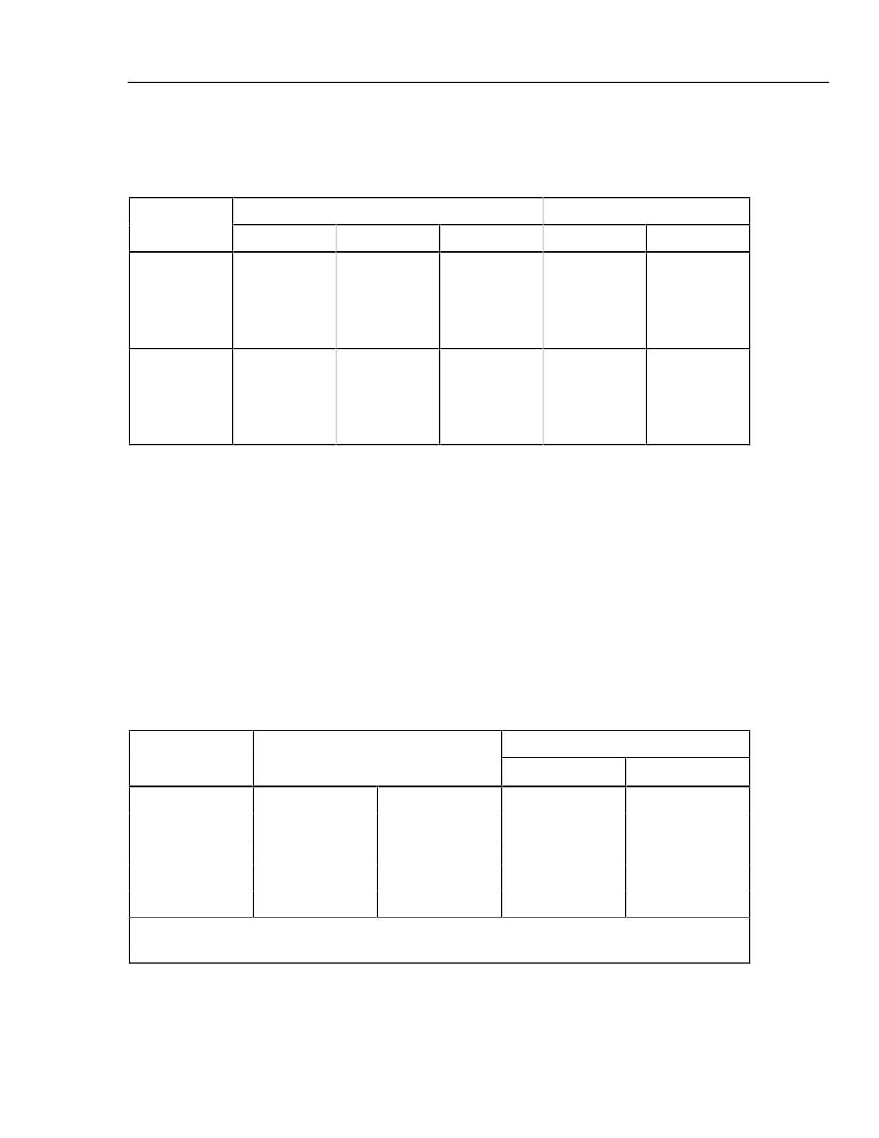
Reading Rates and Display Counts
Rate
Readings per Second
Full Range Display Counts
Slow
2.5
99,999*
Medium
5
30,000
Fast
20
3,000
* Ohms full range will typically be 98,000 counts
1-6
Introduction and Specifications
Specifications
1
Response Times
Refer to Chapter 4 of the Users Manual for detailed information.
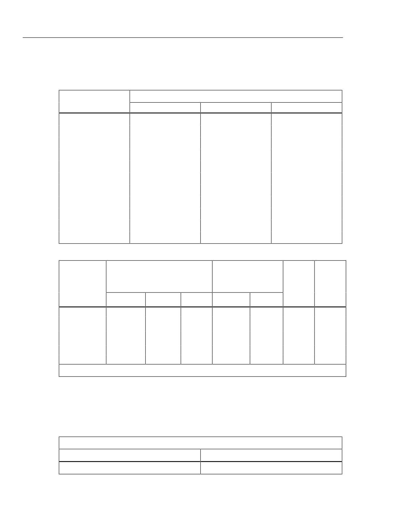
DC Voltage
Resolution
Accuracy
Range
Slow
Medium
Fast
(6 months)
(1 year)
300 mV
-
10 µV
100 µV
0.02% + 2
0.025%+2
3 V
-
100 µV
1 mV
0.02% + 2
0.025% +2
30 V
-
1 mV
10 mV
0.02% + 2
0.025%+2
300 V
--
10 mV
100 mV
0.02% + 2
0.025% +2
1000 V
-
100 mV
1 V
0.02% + 2
0.025%+2
100 mV
1 µV
-
-
0.02% + 6
0.025%+6
1000 mV
10 µV
-
-
0.02% + 6
0.025% +6
10 V
100 µV
-
-
0.02% + 6
0.025%+6
100 V
1 mV
-
-
0.02% + 6
0.025% +6
1000 V
10 mV
-
-
0.02% + 6
0.025%+6
Input Impedance
10 MΩ in parallel with <100 pF
Note
In the dual display mode, when the volts ac and volts dc functions are
selected, the 10 MΩ dc input divider is in parallel with the 1 MΩ ac
divider.
Normal Mode Rejection Ratio
>80 dB at 50 or 60 Hz, slow and medium rates
>54 dB for frequencies between 50-440 Hz, slow and medium rates
>60 dB at 50 Hz, fast rate (Note: Fast rate has no filtering)
Maximum Allowable AC Voltage While Measuring DC Voltage
Peak Normal Mode Signal
Range
Max Allowable Peak AC Voltage
NMRR* >80dB**
NMRR >60 dB**
300 mV
100 mV
20 V
15 V
15 V
3 V
1000 mV
20 V
15 V
15 V
30 V
10 V
1000 V
50 V
300 V
300 V
100 V
1000 V
50 V
300 V
1000 V
1000 V
1000 V
200 V
1000 V
* NMRR is the Normal Mode Rejection Ratio
** Normal Mode Rejection Ratio at 50 or 60 Hz ± 0.1%
Common Mode Rejection Ratio
>90 dB at dc, 50 or 60 Hz, (1 kΩ unbalanced, medium and slow rates)
1-7
45
Service Manual
Maximum Functional Input
1000 V dc or peak ac on any range
True Rms AC Voltage, AC-Coupled
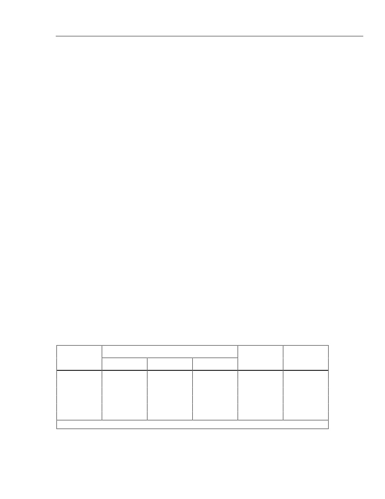
Resolution
Range
Slow
Medium
Fast
300 mV
-
10 µV
100 µV
3 V
-
100 µV
1 mV
30 V
-
1 mV
10 mV
300 V
-
10 mV
100 mV
750 V
-
100 mV
1 V
100 mV
1 µV
-
-
1000 mV
10 µV
-
-
10 V
100 µV
-
-
100 V
1 mV
-
-
750 V
10 mV
-
-
Accuracy
Max Input
Frequency
Linear Accuracy
dB Accuracy
Power*
at Upper
Freq
Slow
Medium
Fast
Slow/Med
Fast
20-50 Hz
1% + 100
1% + 10
7% + 2
0.15
0.72
2% + 10
750 V
50 Hz -10 kHz
0.2% + 100
0.2% + 10
0.5% +
0.08
0.17
0.4% + 10
750 V
2
10 - 20 kHz
0.5% + 100
0.5% + 10
0.5% +
0.11
0.17
1% + 10
750 V
2
20 - 50 kHz
2% + 200
2% + 20
2% + 3
0.29
0.34
4% + 20
400 V
50 - 100 kHz
5% + 500
5% + 50
5% + 6
0.70
0.78
10% + 50
200 V
* Error in power mode will not exceed twice the linear accuracy specification
Accuracy specifications apply within the following limits, based on reading rate:
Slow Reading Rate:
Between 15,000 and 99,999 counts (full range)
Medium Reading Rate:
Between 1,500 and 30,000 counts (full range)
Fast Reading Rate:
Between 150 and 3,000 counts (full range)
Decibel Resolution
Resolution
Slow & Medium
Fast
0.01 dB
0.1 dB
1-8
Introduction and Specifications
Specifications
1
Input Impedance
1 MΩ in parallel with <100 pF
Maximum Crest Factor
3.0
Common Mode Rejection Ratio
>60 dB at 50 or 60 Hz (1 kΩ unbalanced medium rate)
Maximum Input
750 V rms, 1000 V peak
2 x 10⁷ Volt-Hertz product on any range, normal mode input
1 x 10⁶ Volt-Hertz product on any range, common mode input
(AC + DC) Voltage Accuracy
Total Measurement Error will not exceed the sum of the separate ac and dc accuracy
specifications, plus 1 display count. Refer to the table under "Maximum Allowable AC
Voltage While Measuring DC Voltage or (AC + DC) Voltage" located on page 1-6.
Note
When measuring AC + DC, (or any dual display combination of AC and
DC) in the fast reading rate, the Fluke 45 may show significant reading
errors. This results from a lack of filtering on the DC portion of the
measurement for the fast reading rate. To avoid this problem, use only the
"slow" and "medium" reading rates for AC + DC or AC and DC
combinations.
Maximum Frequency of AC Voltage Input While Measuring AC Current
When the meter makes ac current and ac voltage measurements using the dual display,
the maximum frequency of the voltage input is limited to the maximum frequency of the
current function. For example, if you are making an ac current measurement on the 10 A
range, the maximum frequency of the voltage input must be less than 2 kHz.
DC Current
Range
Resolution
Burden
Slow
Medium
Fast
Accuracy
Voltage*
30 mA
-
1 µA
10 µA
0.05% + 3
0.45 V
100 mA
-
10 µA
100 µA
0.05% + 2
1.4 V
10 A
-
1 mA
10 mA
0.2% + 5
0.25 V
10 mA
100 nA
-
-
.05% + 15
0.14 V
100 mA
1 µA
-
-
0.05% + 5
1.4 V
10 A
100 µA
-
-
0.2% + 7
0.25 V
*Typical at full range
1-9
45
Service Manual
Maximum Input
mA
300 mA dc or ac rms. Protected with a 500 mA, 250 V, IEC 127-sheet I,
fastblow fuse and a 440 mA, 1000 V, fast blow fuse.
A
10 A dc ac rms continuous, or 20 A dc or ac rms for 30 seconds maximum.
protected with a 11 A, 1000 V, 17,000 A interrupt rating, fast blow fuse.
Note
Resistance between the COM binding post and the meter’s internal
measuring circuits is approximately .003 Ω
AC Current
Resolution
Range
Burden Voltage*
Slow
Medium
Fast
10 mA
100 µA
-
-
0.14 V
30 mA
-
1 µA
10 µA
0.45 V
100 mA
1 µA
10 µA
100 µA
1.4 V
10 A
100 µA
1 mA
10 mA
0.25 V
* Typical at full range
Accuracy
Accuracy
Range
Frequency
Slow
Medium
Fast
mA (To 100 mA)
20-50 Hz
2% + 100
2% + 10
7% + 2
mA (To 100 mA)
50 Hz - 10 kHz
0.5% + 100
0.5% + 10
0.8% + 2
mA (To 100 mA)
10 - 20 kHz
2% + 200
2% + 20
2% + 3
A (1-10 A)
20 - 50 Hz
2% + 100
2% + 10
7% + 2
A (1 - 10 A)
50 Hz - 2 kHz
1% + 100
1% + 10
1.3% + 2
A (0.5 to 1 A)
20 - 50 Hz
2% + 300
2% + 30
7% + 4
A (0.5 to 1 A)
50 Hz - 2 kHz
1% + 300
1% + 30
1.3% + 4
mA accuracy specifications apply within the following limits, based on reading rate:
Slow Reading Rate:
Between 15,000 and 99,999 counts (full range)
Medium Reading Rate: Between 1,500 and 30,000 counts (full range)
Fast Reading Rate:
Between 150 and 3,000 counts (full range)
1-10
Introduction and Specifications
Specifications
1
Maximum Crest Factor
3.0
Maximum Input
mA
300 mA dc or ac rms. Protected with a 500 mA, 250 V, IEC 127-sheet I, fast
blow fuse and a 440 mA, 1000 V, fast blow fuse.
A
10 A dc or ac rms continuous, or 20 A dc or ac rms for 30 seconds maximum.
Protected with a 11 A, 1000 V, 17,000 A interrupt rating, fast blow fuse.
Note
Resistance between the COM binding post and the meter’s internal
measuring circuits is approximately .003 Ω.
Ohms
Typical
Max Current
Range
Resolution
Accuracy
Full Scale
Through the
Voltage
Unknown
Slow
Medium
Fast
300 Ω
-
10 mΩ
100
0.05% + 2 + 0.02Ω
0.25
1 mA
mΩ
3 kΩ
-
100 mΩ
1Ω
0.05% + 2
0.24
120 µA
30 kΩ
-
1 Ω
10 Ω
0.05% + 2
0.29
14 µA
300 kΩ
-
10 Ω
100 Ω
0.05% + 2
0.29
1.5 µA
3 MΩ
-
100 Ω
1 kΩ
0.06% + 2
0.3
150 µA
30 MΩ
-
1 kΩ
2%
0.25% + 3
2.25
320 µA
300
-
100 kΩ
1 MΩ
2%
2.0
320 µA
MΩ*
100 Ω
1 mΩ
-
-
0.05% + 8 + 0.02Ω
0.09
1 mA
1000 Ω
10 mΩ
-
-
0.05% + 8 + 0.02Ω
0.10
12 µA
10 kΩ
100 mΩ
-
-
0.05% + 8
0.11
14 µA
100 kΩ
1 Ω
-
-
0.05% + 8
0.11
1.5 µA
1000 kΩ
10 Ω
-
-
0.06% + 8
0.12
150 µA
10 MΩ
100 Ω
-
-
0.25% + 6
1.5
150 µA
100 MΩ
100 kΩ
-
-
2% + 2
2.75
320 µA
* Because of the method used to measure resistance, the 100 MΩ (slow) and 300 MΩ(medium and fast)
ranges cannot measure below 3.2 MΩ and 20 MΩ, respectively. "UL" (underload) is shown on the display
for resistances below these nominal points, and the computer interface outputs "+1E-9".
1-11
45
Service Manual
Open Circuit Voltage
3.2 volts maximum on the 100 Ω, 300 Ω, 30 MΩ, 100 MΩ, and 300 MΩ ranges, 1.5
volts maximum on all other ranges.
Maximum Rated Input (Input Protection)
1000 V dc or rms ac on all ranges
Diode Test/Continuity
Maximum Reading
Resolution
Slow
999.99 mV
10 µV
Medium
2.5 V
100 µV
Fast
2.5 V
1 mV
Test Current
Approximately 0.7 mA when measuring a forward-biased junction.
Audible Tone
Continuous tone for continuity. Brief tone for normal forward biased diode or
semiconductor junction.
Open Circuit Voltage
3.2 volts maximum
Continuity Capture Time
50 µs maximum, 10 µs typical
Maximum Rated Input (Input Protection)
1000 volts dc or rms ac
1-12
Introduction and Specifications
Specifications
1
Frequency
5 Hz to > 1 MHz
Applicable Functions
Volts AC and Current AC
Resolution
Range
Accuracy
Slow & Medium
Fast
1000 Hz
.01 Hz
.1 Hz
.05% + 2
10 kHz
.1 Hz
1 Hz
.05% +1
100 kHz
1 Hz
10 Hz
.05% +1
1000 kHz
10 Hz
100 Hz
.05% +1
1 MHz
100 Hz
1 kHz
* For measurement of 1 MHz and lower, accuracy is .05% + 1.
For measurement above 1 MHz, accuracy is not specified.
Sensitivity of AC Voltage
Frequency
Level (Sine Wave)
5 Hz - 100 kHz
30 mV rms
100 kHz - 300 kHz
100 mV rms
300 kHz - 1 MHz
1 V rms
Above 1 MHz
Not Specified
Sensitivity Level of AC Current
Frequency
Input
Level
5 Hz - 20 kHz
100 mA
>3 mA rms
45 Hz - 2 kHz
10 A
>3 A rms
Note
When the meter is set to measure frequency and there is no input signal
(i.e., the input terminals are open), the meter may read approximately 25
kHz (rather than zero). This is due to internal capacitive pickup of the
inverter power supply into the high-impedance, input circuitry. With
source impedance of < 2 kΩ, this pickup will not affect the accuracy or
stability of the frequency reading.
1-13
45
Service Manual
Environmental
Warmup Time
1 hour to rated specifications
Temperature Coefficient
<0.1 times the applicable accuracy specification per degree C for 0°C to 18°C and 28°C
to 50°C
Electromagnetic Compatibility
In an RF field of 1 V/m on all ranges and functions:
Total Accuracy = Specified Accuracy + .4% of range. Performance above 1 V/m is
not specified.
Operating Temperature
0°C to 50°C
Storage Temperature
40°C to + 70°C
Elevated temperature storage of battery will accelerate battery self-discharge. Maximum
storage time before battery must be recharged:
20 - 25°C
1000 days
50°C
180 days
70°C
40 days
Relative Humidity
To 90% at 0°C to 28°C , (non condensing)
To 80% at 28°C to 35°C,
To 70% at 35°C to 50°C except to 70%
at 0°C to 50°C for the 1000 kΩ, 3 MΩ, 10 MΩ, 30 MΩ, 100
MΩ, and 300 MΩ
ranges.
Altitude
Operating
0 to 10,000 feet
Non-operating
0 to 40,000 feet
Vibration
3 G @ 55 Hz
Shock
Half sine 40G. Per Mil-T- 28800D, Class 3, Style E.
Bench Handling. Per Mil-T-28800D, Class 3.
1-14
Introduction and Specifications
Specifications
1
General
Common Mode Voltage
1000 V dc or rms ac maximum from any input to earth
Size
9.3 cm high, 21.6 cm wide, 28.6 cm deep
Weight
Net, 2.4 kg without battery; 3.2 kg with battery; Shipping, 4.0 kg without battery, 4.8
with battery.
Power
90 to 264 V ac (no switching required), 50 and 60 Hz. 15 VA maximum
Safety
Compliant with the following standards:
ANSI/ISA S82.01-1994
CAN/CSA-C22.2 No. 1010. 1-92
EN61010.1:1993 to 1000 V Overvoltage Cat I, 600 V Overvoltage Cat II
UL3111-1. See the following for an explanation of CATI and CATII categories.
CAT I:
OVERVOLTAGE (Installation) CATAGORY I, Pollution Degree 2 per IEC1010-1
refers to the level of Impulse Withstand Voltage protection provided. Equipment of
OVERVOLTAGE CATEGORY I is equipment for connection to circuits in which
measures are taken to limit the transient over voltages to an appropriate low level.
Examples include protect electronic circuits.
CAT II:
OVERVOLTAGE (Installation) CATAGORY II, Pollution Degree 2 per IEC1010-1
refers to the level of Impulse Withstand Voltage protection provided. Equipment of
OVERVOLTAGE CATEGORY II is energy-consuming equipment to be supplied
from the fixed installation. Examples include household, office, and laboratory
appliances.
Electromagnetic Compatibility
Meets FCC Part 15 Subpart J.
EN61326-1 (1998)
RS-232-C
Baud rates:
300, 600, 1200, 2400, 4800 and 9600
Odd, even or no parity One stop bit
1-15
45
Service Manual
Options
Battery (Option -01K)
Type
8 V, Lead-Acid
Operating Time
8 hours (typical). N lights when less than 1/2 hour of battery operation remains. Meter
still meets specifications.
Recharge Time
16 hours (typical) with meter turned off and plugged into line power. Battery will not
charge when meter is turned on.
IEEE-488 (Option -05K)
Capability Codes
SH1, AH1, T5, L4, SR1, RL1, PP0, DC1, DT1, E1, TE0, LE0 and C0 External Trigger
Input VIH 1.35 V minimum VIL 1.25 V maximum
Input Threshold Hysteresis
0.6 V minimum
1-16
Chapter 2
Theory of Operation
Title
Page
2-1.
Introduction
2-3
2-2.
Functional Block Description
2-3
2-3.
Power Supply
2-3
2-4.
Analog Measurement Processor
2-3
2-5.
Input Protection Circuit
2-3
2-6.
Input Signal Conditioning
2-3
2-7.
Analog-to-Digital (A/D) Converter
2-3
2-8.
Serial Communication (Guard Crossing)
2-3
2-9.
Digital Kernel
2-5
2-10.
Display Assembly
2-5
2-11.
IEEE-488 Interface Option (-05)
2-5
2-12.
Battery Pack Option (-01)
2-5
2-13.
Detailed Circuit Description
2-5
2-14.
Power Supply Circuit Description
2-5
2-15.
Raw DC Supply
2-6
2-16.
5-Volt Switching Supply
2-6
2-17.
Inverter
2-7
2-18.
Analog Measurement Processor
2-7
2-19.
Input Protection
2-10
2-20.
Input Signal Conditioning
2-10
2-21.
Relays
2-11
2-22.
DC Volts
2-12
2-23.
Ohms
2-12
2-24.
100 MΩ and 300 MΩ Ranges
2-14
2-25.
AC Volts
2-14
2-26.
DCmA
2-15
2-27.
ACmA
2-15
2-28.
Amps
2-15
2-29.
Diode/Continuity Test
2-15
2-30.
Frequency
2-15
2-31.
Active Filter
2-16
2-32.
A/D Converter
2-17
2-33.
Serial Communication (Guard Crossing)
2-18
2-34.
Digital Kernel
2-18
2-35.
RS-232 Interface
2-19
2-1
45
Service Manual
2-36.
Microprocessor
2-19
2-37.
EEROM
2-19
2-38.
RAM
2-20
2-39.
ROM
2-20
2-40.
IEEE-488 Option Connections
2-20
2-41.
Display Assembly
2-20
2-42.
Main Assembly Connector
2-20
2-43.
Front Panel Switches
2-20
2-44.
Display
2-21
2-45.
Beeper Drive Circuit
2-21
2-46.
Watchdog Timer and Reset Circuit
2-21
2-47.
Display Controller with FIP
2-22
2-2
Theory of Operation
Introduction
2
2-1.
Introduction
This chapter presents a layered description of Fluke 45 circuitry. First, the multimeter is
described in general terms with a Functional Block Description. Then, each block is
detailed further (often to the component level) with Detailed Circuit Descriptions. Refer
to Chapter 9 of this manual for full schematic diagrams.
Signal names followed by a ’*’ are active (asserted) low. Signal names not so marked are
active high.
2-2.
Functional Block Description
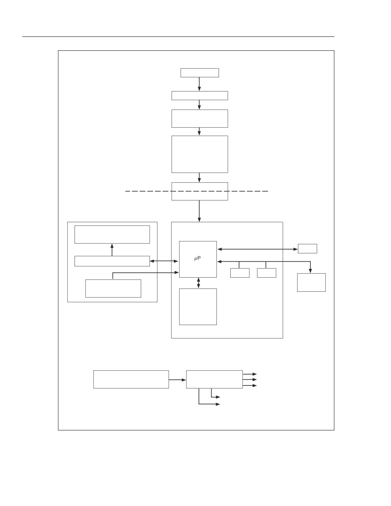
Refer to Figure 2-1, Overall Functional Block Diagram, during the following functional
block descriptions.
2-3.
Power Supply
The Power Supply functional block provides voltages required by both the vacuum-
fluorescent display (-30 V dc, -5.2 V dc, and 5 V ac) and the in-guard circuitry (-5.25 V
dc and 5.25 V dc). Within the Power Supply, the Raw DC Supply converts ac line
voltage to dc levels and the 5 V Switching Supply converts this raw dc to 5 V ±0.25 V
dc, which is used by the Inverter in generating the above-mentioned outputs.
2-4.
Analog Measurement Processor
The Analog Measurement Processor (A1U1) provides input signal conditioning, ranging,
a/d conversion, and frequency measurement. This custom chip is controlled by the Main
Processor (A1U6), with communication carried out over a special serial interface.
2-5.
Input Protection Circuit
Input protection safeguards the meter against a number of over-voltage and over-current
conditions. Depending on the type of input, protection circuits or fuses are used.
2-6.
Input Signal Conditioning
The input signal (voltage, current, or resistance) must be scaled or conditioned to a dc
voltage that can be measured by the a/d converter. High dc voltage levels must be
attenuated. Resistances, currents, and ac voltages must be converted to a representative
dc voltage. DC-type measurements (dc volts, dc current, ohms, and diode test) are then
filtered by an active filter. AC measurements (ac volts and ac current) are passively
filtered after being converted to a dc voltage.
2-7.
Analog-to-Digital (A/D) Converter
The voltage level from the signal conditioning circuits charges (or integrates) a capacitor
for an exact amount of time. The capacitor discharge time, which is proportional to the
level of the unknown input signal, is measured by the digital circuits in the Analog
Measurement Processor and sent to the microprocessor.
2-8.
Serial Communication (Guard Crossing)
This functional block provides a high isolation voltage communication path between the
Digital Kernel and the Analog Measurement Processor. This bi-directional
communication circuit also requires power supply voltages from the Power Supply
block.
2-3
45
Service Manual
Inputs
Input Protection
Input Signal
Conditioning
Analog
Measurement
Processor
(A/D Converter)
Serial
Guard
Communication
Crossing
Vacuum Fluorrescent
Display
RS-232
Display Controller
RAM
ROM
IEEE-488
Front Panel
Option -05
Switches
EEPROM
Display Assembly
Calibration
Constants
Digital Kernel
5 Vac
Battery Assembly
Power
-5.2 Vdc
Option -01
Supply
-30 Vdc
5.25 Vdc
-5.25 Vdc
qb01.eps
Figure 2-1. Overall Functional Block Diagram
2-4
Theory of Operation
Detailed Circuit Description
2
2-9.
Digital Kernel
The Digital Kernel functional block is responsible for the coordination of all activities
within the meter. This block requires power supply voltages from the Power Supply and
reset signals from the Display Assembly.
Specifically, the Digital Kernel Microprocessor performs the following functions:
• Executes the instructions in ROM
• Stores temporary data in RAM
• Store meter configuration and calibration data in EEROM
• Communicates with the Analog Measurement Processor via the Serial
Communication (Guard Crossing) block
• Communicates with the Display Controller to display readings and user interface
information
• Scans the user interface keyboard found on the Display Assembly
• Communicates via the RS-232 interface and optional IEEE-488 interface.
2-10.
Display Assembly
The Display Assembly controller communicates with the main Microprocessor over a
three-wire communication channel. Commands from the Microprocessor inform the
Display Controller how to modify its internal display memory. The Display Controller
then drives the grid and anode signals to illuminate the required segments on the
Display. The A2 Display Assembly requires power supply voltages from the Power
Supply and a clock signal from the A1U6 Microprocessor.
2-11.
IEEE-488 Interface Option (-05)
Theory of operation for the IEEE-488 Interface Option (-05) is presented in Chapter 8 of
this manual. The related schematic diagram is found in Chapter 9.
2-12.
Battery Pack Option (-01)
Chapter 7 of this manual contains the theory of operation for the Battery Pack Option
(-01). Refer to Chapter 9 for the related schematic diagram.
2-13. Detailed Circuit Description
2-14. Power Supply Circuit Description
The Power Supply consists of the following three functional sections:
• Raw DC Supply
The Raw DC Supply converts line voltage (90 V to 264 V ac) to a dc output of 7.5 V
to 5 V.
•
5 V Switching Supply
The 5 V Switching Supply converts the Raw DC Supply output to 5.1 V ± 0.25 V dc.
• Inverter
Using the 5 V Switching Supply output, the Inverter generates the -30 V dc, -5 V dc,
and 5 V ac supply levels needed for the vacuum-fluorescent display. Also, the
2-5
45
Service Manual
Inverter provides isolated positive and negative 5.25 V outputs for the in-guard
circuitry.
2-15.
Raw DC Supply
The Raw DC Supply uses a power transformer (A1T3) that operates on input line
voltages ranging from 90 V to 264 V ac. Since there is no power switch in the
transformer input circuit, the Raw DC Supply is energized whenever the meter is
connected to line power. The transformer uses an internal 275 V ac MOV (metal-oxide
varistor) to clamp line transients. This MOV normally acts as an open circuit; when the
peak voltage exceeds approximately 400 V, the MOV turns on and, working with the
line impedance in series with the line fuse, limits the transient peak voltage to 400 to 500
V. All line voltages use a T 0.125 A, 250 V (slow blow) fuse.
On the secondary side of the transformer, the output is rectified by diodes A1CR2 and
A1CR3 and filtered by capacitor A1C27. In addition, A1C26 reduces rectifier diode
switching emi emissions from the meter. The meter power switch (A1S1) is also
connected in the output of the Raw DC Supply; it connects the Raw DC Supply either to
the 5-V Switching Supply (when the meter is ON) or to the Battery Charger Switching
Supply through A1J1-7 (when the meter is OFF.)
2-16.
5-Volt Switching Supply
The 5-Volt Switching Supply incorporates the A1U11 controller device and several
external components. Operating on an input of 7.5 V dc to 35 V dc, the 5-volt Switching
Supply uses a pulse-width modulation technique to regulate its output at 5.1 V dc. The
nominal switching frequency is 40 kHz.
With the controller, the output voltage is controlled by varying the duty cycle (ON time)
of the switch transistor in A1U11. (Controller device A1U11 contains the supply
reference, oscillator, switch transistor, pulse-width modulator comparator, switch drive
circuit, current-limit comparator, and current-limit reference.) Resistors A1R41 and
A1R42, in conjunction with the reference circuit, set the input levels to the pulse-width
modulating comparator. Resistors A1R35 (in parallel with A1R41) and A1R36 (in
parallel with A1R42) are used in production to adjust the 5.1 V supply output. Removing
A1R35 decreases the output by approximately 5%. Removing A1R36 increases the
output by approximately 7%.
Within the controller, the output of the comparator is combined with the oscillator signal
to form the drive signal for the switch transistor. Diode A1CR6 operates as a
complementary switch with the switch transistor. Dual inductor A1T1 is a magnetic
device that regulates current pulses as the switch transistor is turned on and off. A
current shunt (A1R47, A1R48, and A1R49) senses the overall current flowing through
diode A1CR5 and the switch transistor of A1U11. If this current rises too high, the duty
cycle (ON time) of the switch transistor is reduced to current-limit the supply. Capacitor
A1C33 serves as a filter capacitor and energy storage device, and A1C34 and A1C35 are
the output filter capacitors.
The boost circuit (A1CR4 and A1C32) supplies the controller A1U11 with sufficient
supply voltage when the switching supply input is low. For example, this condition may
occur when the meter is operating on low line voltage.
Resistor A1R40 and capacitors A1C28 and A1C29 are needed for proper dynamic
performance of the switching supply. Capacitor A1C30 sets the operating frequency of
the supply.
2-6
Theory of Operation
Detailed Circuit Description
2
2-17.
Inverter
The inverter uses transistors A1Q10, A1Q11, A1Q12, and A1Q13 connected to form an
astable 30-kHz multivibrator. The operating frequency and drive to the transistors are
determined by the values of the interconnecting resistors and capacitors. The inverter
transformer (A1T2) primary is connected across the collectors of the multivibrator
transistors; the primary winding is thereby driven by a symmetrical square wave.
Resistor A1R46 and capacitor A1C41 form a filter network to reduce the amplitude of
current pulses generated by the switching of the inverter transistors.
The secondary windings of A1T2 are used for three sets of supply voltages. The first
winding of the A1T2 secondary provides out-guard outputs using the following rectifier
diodes and filter capacitors to provide the required voltages for the display and the
battery trickle charger circuit.
• A1CR11 and A1C45: -30 V supply
• A1CR12 and A1C47: -5 V supply
• A1CR10 and A1C46: +30 V source for the battery trickle charger.
Next, an isolated secondary winding provides the various in-guard supplies. Dual diodes
A1CR8 and A1CR9 and capacitors A1C43 and A1C44 are the rectifiers and filters for
the in-guard +5.25 V and -5.25 V supplies. Dual diode A1CR7 and capacitor A1C42 are
the rectifier and capacitor for the relay (5.25 V dc) supply.
A third transformer winding provides the heater power (FIL1, FIL2) for the vacuum-
fluorescent display. Zener diode A1VR3 and resistor A1R55 bias this winding at
approximately 5 volts more positive than the -30 V supply.
2-18.
Analog Measurement Processor
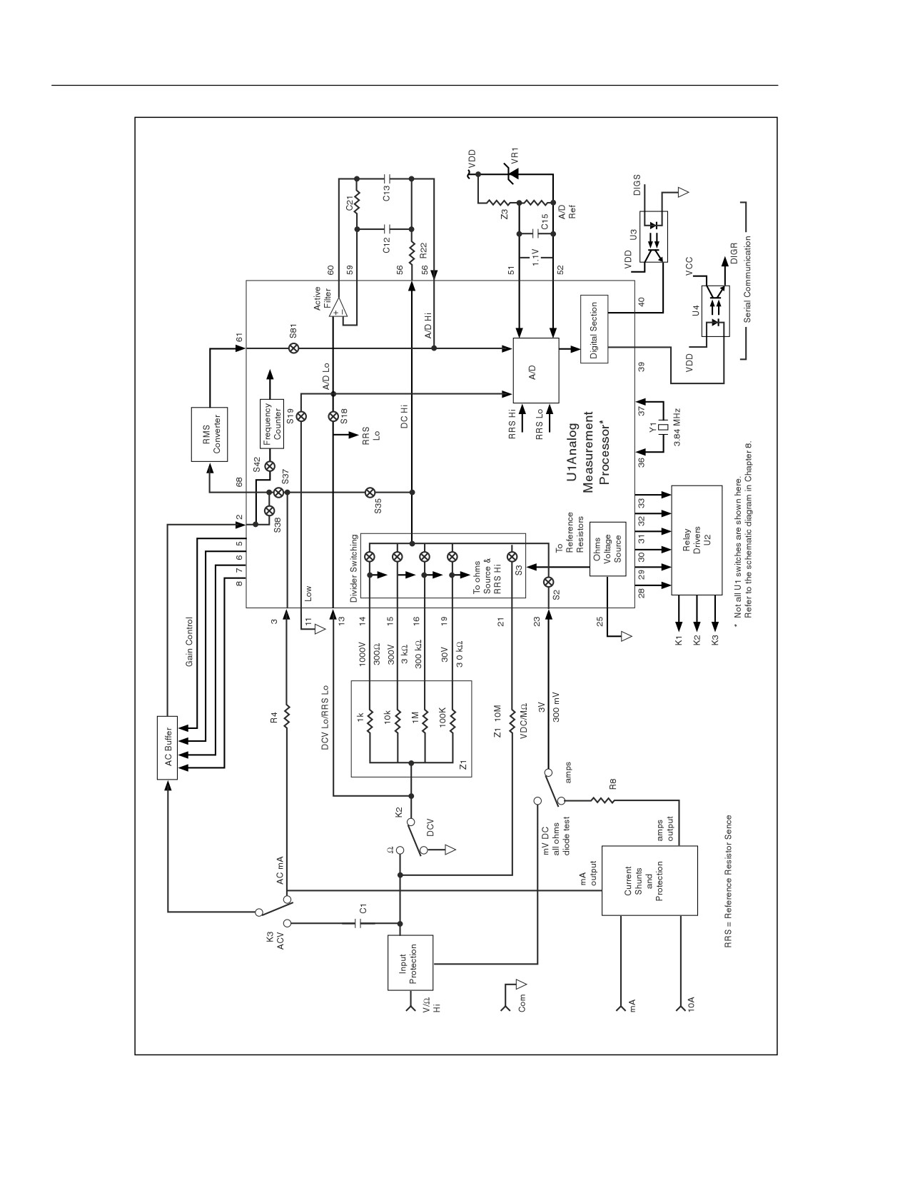
Refer to Figure 2-2 for an overall picture of the Analog Measurement Processor chip and
its peripheral circuits. Table 2-1 describes Analog Measurement Processor chip signal
names.
The Analog Measurement Processor (A1U1) is a 68-pin CMOS device that, under
control of the Main Processor (A1U6), performs the following functions:
• Input signal routing
• Input signal conditioning
• Range switching
• Active filtering of dc-type measurements. The active filter is disabled for fast
reading rate measurements.
• A/D conversion
• Support for direct volts, direct current, true rms alternating volts, true rms alternating
current, ohms, frequency, and continuity/diode test functions.
Two separate signal paths are used, one for dc/ohms and one for ac. For dc, the 3 V
range and below are coupled directly to the a/d converter; higher voltages are attenuated.
For ohms, the dc circuitry is augmented with an internal ohms source voltage regulator
controlled through an extra set of switches. For ac, inputs are routed through the ac
buffer, with attenuation being controlled by the a/d converter.
The a/d converter uses a modified dual-slope minor cycle method. The basic
measurement unit, a minor cycle, consists of a fixed time integrate period for the
unknown input, a variable reference integrate period, a variable hold period, and various
short transition periods. A minor cycle period equals 25 ms.
2-7
45
Service Manual
qb02f.eps
Figure 2-2. Analog Simplified Schematic Diagram
2-8

Theory of Operation
Detailed Circuit Description
2
Table 2-1. Analog Measurement Processor Pin Name Description
Pin
Name
Description
1
VDD
+5 V supply
2
ACBO
AC buffer output
3
AIN
Amps input
4
AGND2
Analog ground #2
5
ACR4
AC buffer range 4
6
ACR3
AC buffer range 3
7
ACR2
AC buffer range 2
8
ACR1
AC buffer range 1
9
VSSACR
-5 V supply for AC ranging
10
(not used)
11
LO
A/D converter low input
12
GRD
Guard
13
RRS
Reference resistor sense for ohms
14
V4
Tap #4 on the DCV input divider/ohms reference network
15
V3
Tap #3 on the DCV input divider/ohms reference network
16
V1
Tap #1 on the DCV input divider/ohms reference network
17
GRD
Guard
18
V2F
Tap #2 active filter input on the DCV input divider/ohms reference network
19
V2
Tap #2 on the DCV input divider/ohms reference network
20
GRD
Guard
21
V0
Tap #0 on the DCV input divider/ohms reference network
22
GRD
Guard
23
OVS
Ohms and volts sense input
24
GRD
Guard
25
AGND1
Analog ground #1
26
(not used)
27
DGND
Digital ground
28
FC0
Function control #0
29
FC1
Function control #1
30
FC2
Function control #2
31
FC3
Function control #3
32
FC4
Function control #4
33
FC5
Function control #5
34
FC6
(not used)
35
FC7
(not used)
36
OSCIN
Crystal oscillator input
37
OSCO
Crystal oscillator output
38
MRST
Master reset
39
AS
Analog send
40
AR
Analog receive
41
SK
Serial clock
42
CS
Chip select
43
BRS
Baud rate select
44
VSS
-5 V
45
INT
Integrator output
46
SUM
Integrator summing node
47
B.1
Buffer output, 100 mV range
48
B.3
Buffer output, 300 mV range
49
B1
Buffer output, 1000 mV range
50
B3
Buffer output, 3 V range
2-9

45
Service Manual
Table 2-1. Analog Measurement Processor Pin Name Description (cont)
Pin
Name
Description
51
VREF+
A/D reference plus
52
VREF-
A/D reference minus
53
RAO
A/D reference amplifier output
54
RA+
A/D reference amplifier noninverting input
55
RA-
A/D reference amplifier inverting input
56
AFO
Active filter output
57
MOF
Megohms filter
58
AFI
Active filter input
59
FAI
Filter amplifier inverting input
60
FAO
Filter amplifier output
61
RMSF
RMS output, filtered
62
ARTN
Analog return
63
(not used)
64
RMSO
RMS converter output
65
BIAS2
Bias input
66
VSSF
-5 V dc, filtered
67
BIAS1
Bias input
68
RMSI
RMS converter input
2-19.
Input Protection
Input protection safeguards the meter against a number of over-voltage and over-current
conditions. The various input protection schemes are as follows:
• In the Voltage mode of operation, MOVs A1RV1, A1RV2 and A1RV3 clamp input
voltage transients to about 1800 volts, and A1R5, A1RT1 and A1R6 limit the
current. In this mode, A1R7 and the 10-MΩ resistor in A1Z1 protect A1U1.
• In the Ohms and Diode Test modes, A1Q1 clamps voltage inputs of both polarities,
and A1R5 and thermistor A1RT1 limit the overload current. With large overloads,
A1RT1 heats up and increases in resistance. Components A1R9 and A1Z1 protect
A1U1.
• The [100 mA] input is protected by fuses F1 and F5. With this input, A1R4 protects
A1U1.
• The [10 A] input is protected by fuse A1F2, with A1R8 protecting A1U1.
2-20.
Input Signal Conditioning
The input signal (voltage, current, or resistance) must be scaled or conditioned to a form
that can be measured by the a/d converter. High dc voltage levels must be attenuated.
Resistances, currents, and ac voltages must be converted to a representative dc voltage.
DC-type measurements (dc volts, dc current, ohms, and diode test) are then filtered by
the active filter. AC measurements (ac volts and ac current) are passively filtered after
being converted to a dc voltage. In the medium and fast measurement rates, the a/d
converter uses one of two ranges: ±300 mV and ±3 V full scale. In the slow rate, the a/d
converter uses one of two additional ranges (±100 mV and ±1000 mV full scale), for a
total of four ranges.
2-10
Theory of Operation
Detailed Circuit Description
2
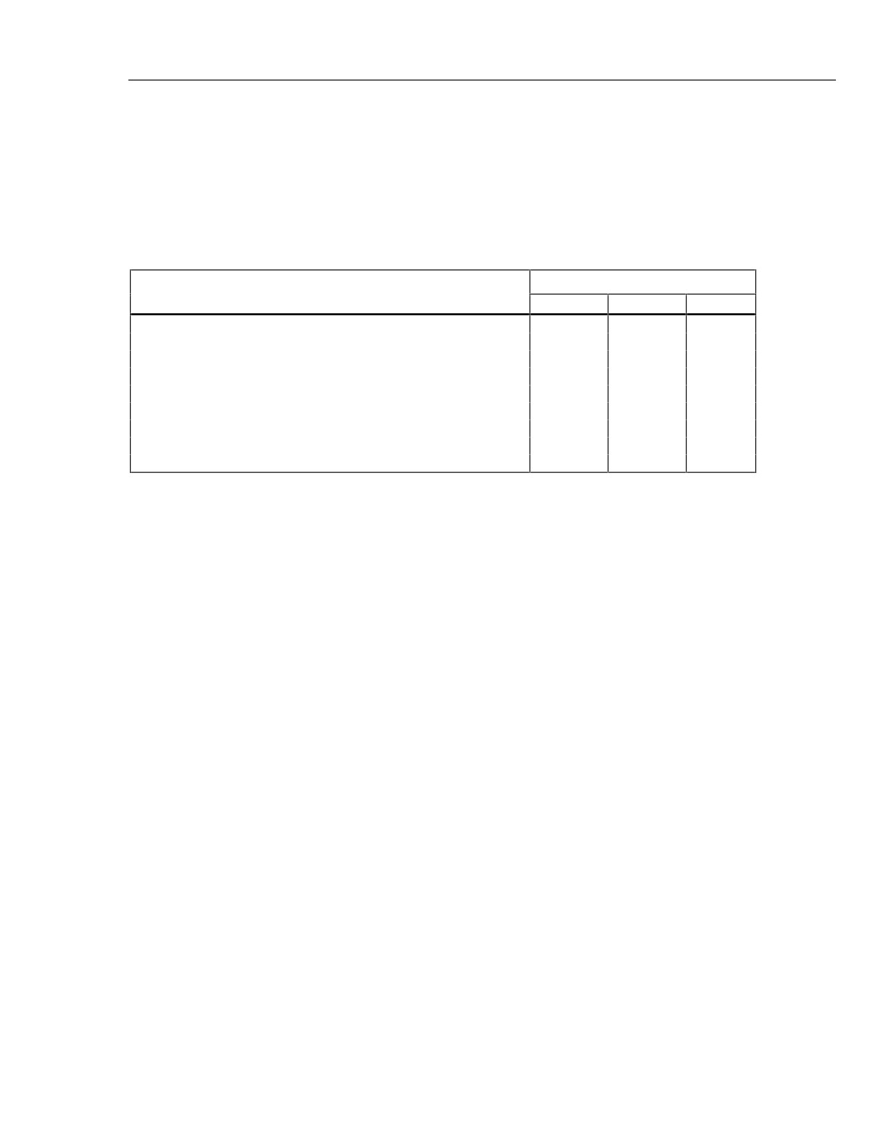
2-21. Relays
Latching relays A1K1, A1K2, and A1K3 route and connect the input signal to the
functional blocks required by the selected function. The Analog Measurement Processor
(A1U1) function control outputs, which are 8-ms positive pulses (0 V to VDD) at FC0 to
FC5 (pins 28 to 33), control the relay driver, A1U2. The A1U2 drivers are NPN
Darlington pairs. Relay functions are defined in Table 2-2.
Table 2-2. Relay Operation
Relays
Function
A1K
A1K2
A1K3
DC mV, 3 V
Reset
Set
Set
DC 10 V, 30 V, 100 V, 300 V, 1000 V
Set
Set
Set
ACV
Set
Set
Reset
Ohms & k ohms
Reset
Reset
Set
M ohms
Reset
Set
Set
Diode Test
Reset
Reset
Set
mA DC and ADC
Set
Set
Reset
mA AC and AAC
Set
Set
Set
Frequency
Set
Set
Reset
2-11
45
Service Manual
S2
A1R6 &
A1R7
A1K1
VΩ
A1R5 &
A1RT1
A1Z1
10M
S3
S9
S10
ACTIVE
HIGH
FILTER
A1Z1
A/D
10.01k
A1R9
LOW
A1K2
COM
qb03f.eps
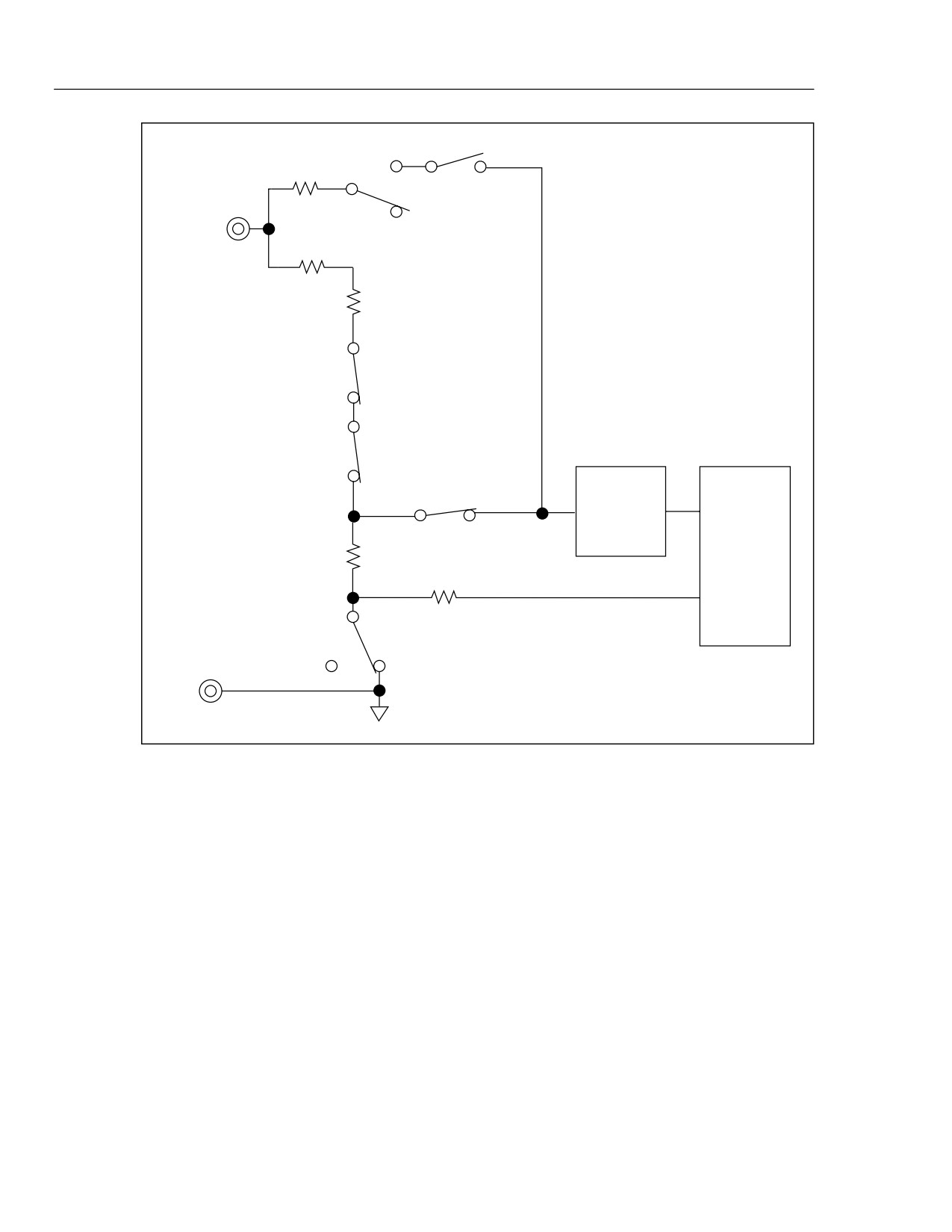
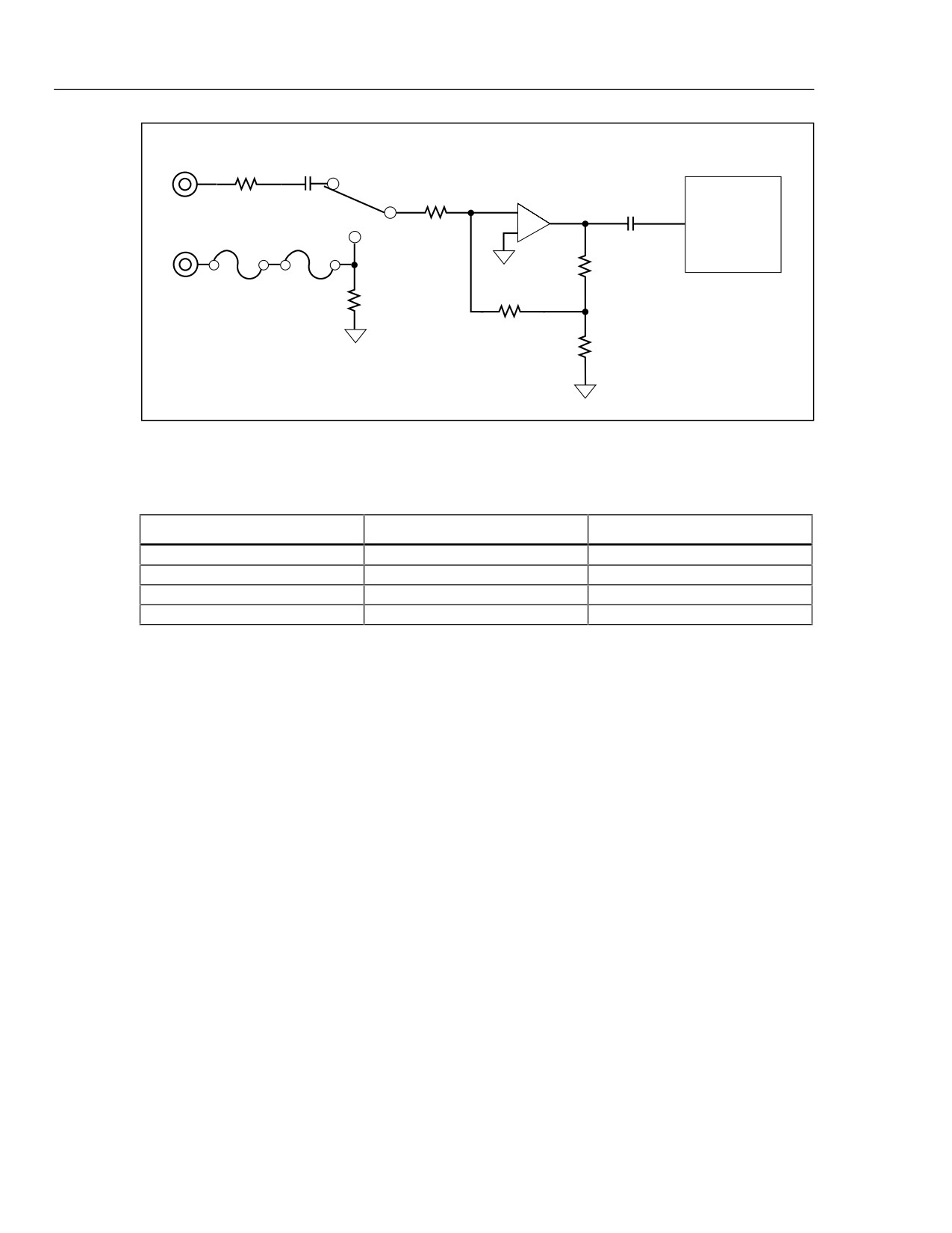
Figure 2-3. DC Volts 300 V Range Simplified Schematic
2-22. DC Volts
For the mV and 3 V ranges, the input signal is applied to A1U1 through A1R6, A1R7,
and A1K1. The signal is routed directly through A1U1 to the active filter and the a/d
converter without attenuation. Higher voltages are attenuated by the dc input divider
A1Z1.
For the 300 V range, switches S3 and S9 in A1U1 connect the A1Z1 10-MΩ resistor to
the A1Z1 10.01-kΩ resistor, forming a 1000:1 divider. See Figure 2-3. The S10 switch in
A1U1 routes the signal to the active filter. Pin 3 of A1Z1 serves as divider common,
which is also the a/d converter low signal sensed through A1R9.
2-23. Ohms
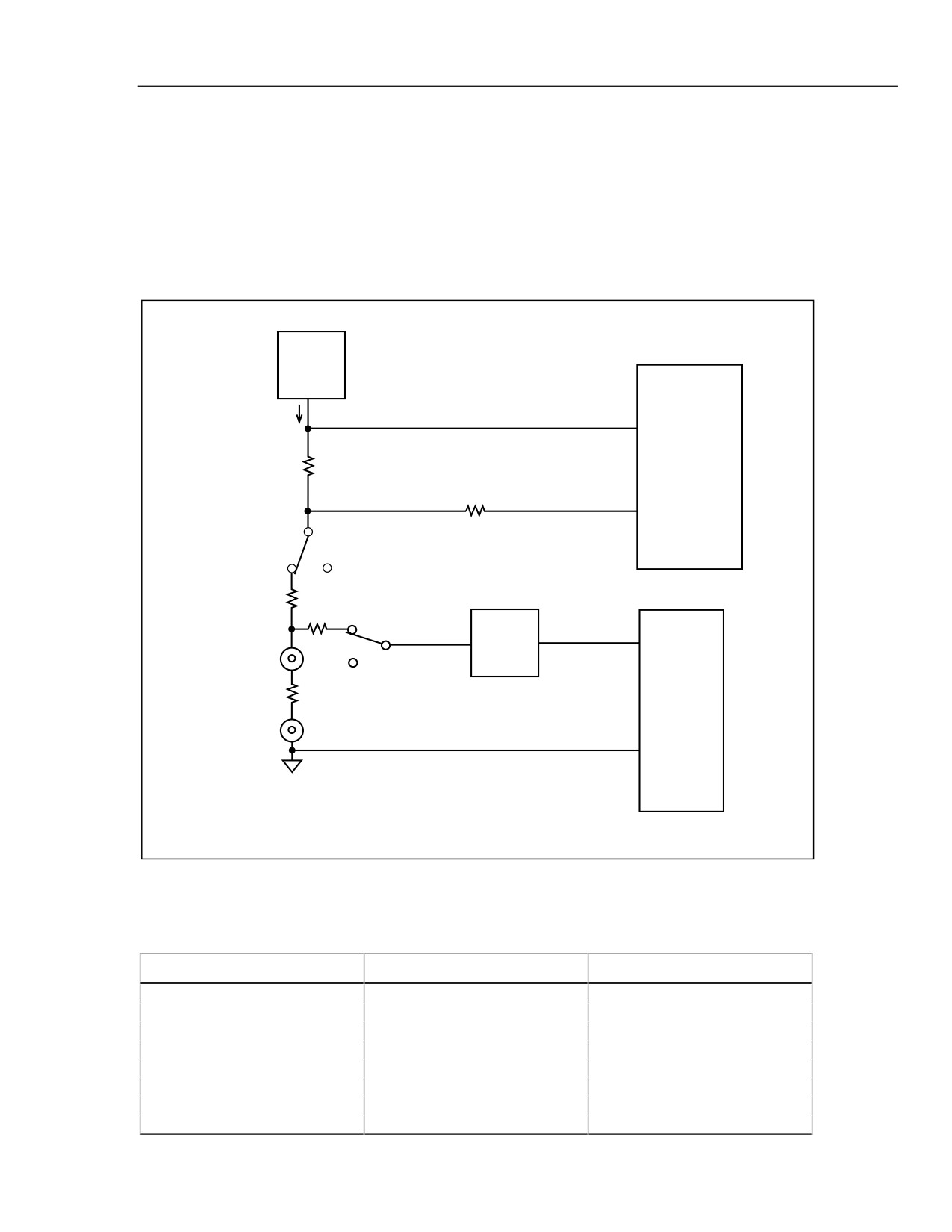
Resistance measurements are made using the ratio ohms technique. See Figure 2-4. A
voltage source is connected in series with the reference resistor (A1Z1) and the unknown
resistor. Since the same current then flows through both resistors, the unknown
resistance is determined from the ratio of the voltage drops across the reference and
unknown resistors.
2-12
Theory of Operation
Detailed Circuit Description
2
Depending on the range, S3, S6, S9, S13, or S15 connects the Analog Measurement
Processor ohms voltage source to a reference resistor. The resulting current passes
through the reference resistor, A1K2, the protection resistors A1RT1 and A1R5, and the
unknown resistance. The a/d converter integrates with the voltage across the unknown
through the OVS input (pin 23). For DE- integrate reference, the a/d converter uses the
voltage across the reference resistor through RRS (pin 13) and Ohms Reference High
through S5 (pin 21), S14 (pin 19), S17 (pin 16), S11 (pin 15) or S8 (pin 14). Reference
resistances are identified in Table 2-3.
OHMS
VOLTAGE
SOURCE
IX
LOW
A/D
+
A1Z1
RREF
INTEGRATE
VR REF
REFERENCE
_
REFERENCE
RESISTOR
A1R9
HIGH
A1K2
A1RT1&A1R5
A1R6 & A1R7
ACTIVE
HIGH
A1K1
FILTER
V Ω
+
RX
A/D
VR X UNKNOWN
INTEGRATE
RESISTOR
UNKNOWN R
COM
LOW
VR X
IXRX
RX
=
VR REF =
IX RREF RREF
qb04f.eps
Figure 2-4. Ohms Simplified Schematic
Table 2-3. Reference Resistance
Range
Voltage Source
A1Z1 Reference Resistor
100 Ω /300 Ω
3 V
1 kΩ
1000 Ω/3 kΩ
1.3 V
10.01 kΩ
10 kΩ/30 kΩ
1.3 V
100.5 kΩ
100 kΩ/300 kΩ
1.3 V
1 MΩ
1000 kΩ/3 MΩ/10 MΩ
1.3 V
10 MΩ
30 MΩ
3 V
10 MΩ
100 MΩ/300 MΩ
3 V
10 MΩ
Diode Test
3 V
1 kΩ
2-13
45
Service Manual
A1R5 &
V
A1RT1
A1C1
A1Z2
A1K3
1.111M
A1AR1
_
A1C7
RMS
+
F1
F5
COVERTER
mA
A1Z2
2.776k
A1R2
10
A1Z2 FEEDBACK
A1Z2
RESISTOR
115.7
qb05f.eps
Figure 2-5. AC Buffer Simplified Schematic
Table 2-4. AC Volts Input Signal Dividers
Range (Drive Signal)
A1Z2 Feedback Resistor
Overall Gain
100/300 mV (ACR1)
111.1 kΩ
2.5
1000 mV/3 V (ACR2)
12.25 kΩ || 111.1 kΩ
.25
10/30 V (ACR3)
1.013 kΩ || 111.1 kΩ
.025
100/300/750 V (ACR4)
2.776 kΩ
.0025
2-24.
100 MΩ and 300 MΩ Ranges
The 100 MΩ and 300 MΩ ranges perform a conductance reading; the mathematical
reciprocal of this reading is used as a display in ohms. The reference resistor (A1Z1, 10
MΩ) is integrated first, then the unknown resistance is used for DE- integrate reference.
2-25.
AC Volts
AC voltage and ac current inputs are scaled by the ac buffer, then converted to a
representative dc voltage by the true rms ac-to-dc converter.
Refer to Figure 2-5. JFETs A1Q2 to A1Q8 switch the ranges of the buffer amplifier
A1AR1. The JFET drive signals, ACR1 to ACR4 (pins 5 to 8) turn the JFETs either on at
0 V or off at -VAC. The ratio of the feedback resistor to the 1.111-MΩ input resistor
divides the input signal by 10, 100, or 1000. These arrangements are summarized in
Table 2-4. This signal is then amplified by 25 using the 2.776-kΩ and 115.7Ωbuffer
output divider resistors. The A1Z2 111.1-kΩ feedback resistor is left in parallel with the
higher range feedback resistors. For the 300/750 V range, the 2.776-kΩresistor becomes
the feedback element. A1R15 and A1C2 compensate the 300-mV range of the ac buffer.
The ac signal is then routed to the rms converter by Analog Measurement Processor
switch S38. Capacitors A1C1, A1C7, A1A1C2, and A1A1C3 function as dc blocking
capacitors. A1A1R1 provides input bias current for the rms converter buffer, and
A1A1C1 is the converter’s averaging capacitor.
The rms converter output is divided down by 2.5 by A1Z4; A1R19 and A1C10 form the
passive filter for ac volts. Analog Measurement Processor switch S80 shorts A1R19 both
during ranging and in the fast measurement rate. Components A1R16, A1R17, A1C3,
2-14
Theory of Operation
Detailed Circuit Description
2
A1C4, A1C5, and A1C6 provide a filtered power supply for the ac buffer, the ac buffer
switching JFETs, and the rms converter.
2-26.
DCmA
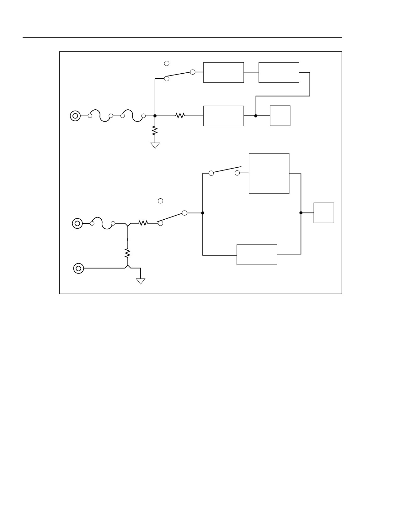
Current through A1R2 develops a voltage that is proportional to the input. This dc
voltage is routed through A1R4 to the active filter, then to the a/d converter. The 100
mA current range uses the 3 V range of the a/d converter. See Figure 2-6.
2-27.
ACmA
In ACmA, relay A1K3 connects the ac voltage developed across A1R2 to the ac buffer.
The signal is then conditioned as described for ac volts.
2-28.
Amps
The dc voltage output of the 10 amp shunt (A1R3) is routed directly to the a/d converter
through the Analog Measurement Processor OVS input (pin 23). For ac amps, the ac
voltage output of the shunt is routed to the rms converter through Analog Measurement
Processor switches S35 and S37.
2-29.
Diode/Continuity Test
In Diode Test, the meter front end is in the 300 ohm range configuration. The a/d
converter measures the dc voltage at the binding posts through the OVS input (pin 23).
For the continuity function, the frequency/continuity comparator senses the signal
through Analog Measurement Processor switches S35 and S41. The comparator toggles
when the input goes below about 20 mV.
2-30.
Frequency
The frequency/continuity comparator uses the ac volts/ac mA output of the ac buffer as
its input at the Analog Measurement Processor ACBO input (pin 2). In the 10 A ac
range, the signal is routed to the comparator through Analog Measurement Processor
switches S35 and S41.
2-15
45
Service Manual
A1K3
AC
RMS
BUFFER
CONVERTER
RESET
mA
F1
F5
A1R4
ACTIVE
A/D
FILTER
A1R2
10
S36
RMS
ACA
CONVERTER
A1K1
10A
A1F2
A/D
A1R8
A1R3
DCA
ACTIVE
COM
.01
FILTER
qb06f.eps
Figure 2-6. DC mA and Amps Simplified Schematic
2-31. Active Filter
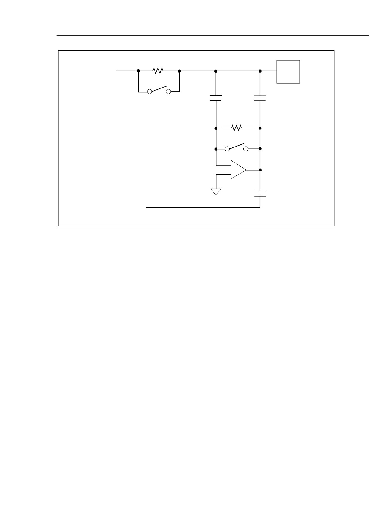
Refer to Figure 2-7. The two-pole active filter consisting of A1R21, A1R22, A1C12, and
A1C13 filters noise on the a-d converter input signal for the DCV, DCmA, DCA,
OHMS, kOHMS, and Diode Test functions. Resistor A1R22 provides a 200-kΩ input
impedance for the filter, except as follows:
• Resistors A1R6 and A1R7 provide the 200-kΩ input impedance for the 100 mV dc,
300 mV dc, 1000 mV dc, 3 V dc, ohms, and kilohms ranges.
• Resistor A1R10 and the 100.5 kΩ resistor in A1Z1 provide the 200 kΩ impedance
for the 10 V and 30 V dc ranges.
• Resistor A1R4 provides the impedance for the two DCmA ranges.
Analog Measurement Processor switch S82 shorts out A1R21 during ranging. Switch
S87 shorts out A1R22 both during ranging and in the measurements listed above. For the
1000 kΩ, 3 MΩ, 10 MΩ, 30 MΩ, 100 MΩ, and 300 MΩ ranges, the active filter is
bypassed, and switch S83 selects C14 as the filter.
2-16
Theory of Operation
Detailed Circuit Description
2
A1R22
ACTIVE
FILTER
A/D
INPUT
A1C12
A1C13
S87
A1R21
S82
_
+
A1C14
MW
FILTER
qb07f.eps
Figure 2-7. Active Filter Simplified Schematic
2-32.
A/D Converter
Figure 2-8 shows the dual slope a/d converter used in the Fluke 45. A voltage level
proportional to the unknown input signal charges (integrates) a capacitor for an exact
amount of time. This capacitor is then discharged by a reference voltage of opposite
polarity. The capacitor discharge time, which is proportional to the level of the unknown
input signal, is measured by the digital circuits in the Analog Measurement Processor
and sent to the microprocessor.
In the medium and fast measurement rates, the a/d converter uses the ±300 mV or ±3 V
range. These ranges typically uprange at a display of 32,000 in the medium rate. In the
slow rate, the a/d converter uses one of two additional ranges: ±100 mV and ±1000 mV.
The uprange point for these additional ranges is a display of 99,999. In the ohms
function only, a typical uprange point is a display of about 98,000.
During the integrate phase, the a/d buffer in Analog Measurement Processor A1U1
applies the signal to be measured to one of the four integrate resistors in resistor network
A1Z3. The choice of resistor depends on the measurement range. Switch S69 connects
output B.1 (pin 47) for the 100-mV range; S71 uses output B.3 (pin 48) for the 300-mV
range; S73 uses output B1 (pin 49) for the 1000 mV range; and S75 uses output B3 (pin
50) for the 3 V range. Refer to Figure 8-1.
The current through the selected integrator resistor charges integrator capacitor A1C16.
After the integrate phase, the buffer applies the opposite polarity reference voltage, and
the integrator integrates back down until the comparator toggles. A counter measures the
integrate reference time. If the a/d converter is overloaded and the integrator does not
return to its starting point by the end of the integrate reference phase, S77 discharges
integrator capacitor A1C16.
The reference voltage for volts, current, and diode test modes is provided by a 6.3 V
zener diode, A1VR1. The reference amplifier in the Analog Measurement Processor
2-17
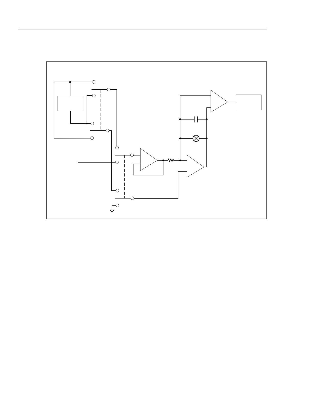
45
Service Manual
provides 2 mA of current through A1VR1. Resistor network A1Z3 divides the 6.3 V
down to 1.1 V.
+ REFERENCE
(- INPUT)
+
+
REFERENCE
COUNTER
_
_
A1C16
A/D
COMPARATOR
S77
INTREGRATE
REFERENCE
-REFERENCE
(+ INPUT)
+
A1Z3
_
INPUT
_
BUFFER
+
INTEGRATOR
INTEGRATE
INPUT
qb08f.eps
Figure 2-8. A/D Converter Simplified Schematic
2-33.
Serial Communication (Guard Crossing)
The Microprocessor communicates with the Analog Measurement Processor using this
isolated two-wire, full-duplex asynchronous interface circuit.
When the Microprocessor is transmitting to the Analog Measurement Processor, the
transmit data bits appear at A1U6-11, which drives the combination of AQ19, A1R33
and A1U3-1. The optocoupler A1U3 then optically transfers this information to its
output circuit, comprised of A1U3-7, A1R30, A1R28 and A1R27. The transmitted data
is then presented to A1TP4 and A1U1-40.
When the Analog Measurement Processor is transmitting data back to the
Microprocessor, the data bits appear at A1U1-39, which drives the input of a Darlington
driver A1U2-1. The Darlington driver output then drives A1R29 and A1U4-1 to transfer
the information to the output of the optocoupler at A1U4-7. Resistors A1R32 and A1R34
complete the optocoupler output circuit. Data is then routed to A1TP7 and A1U6-10 on
the Microprocessor.
2-34.
Digital Kernel
The Digital Kernel is composed of six functional circuit blocks: the RS-232 interface,
the Microprocessor, the EEROM (Electrically Erasable Read Only Memory), the RAM
(Random Access Memory), the ROM (Read Only Memory), and the IEEE-488 Option
Connections. These blocks are described in the following paragraphs.
2-18
Theory of Operation
Detailed Circuit Description
2
2-35.
RS-232 Interface
The RS-232 interface is composed of connector A1J5, RS-232 level shifter A1U7 and
the hardware serial communication interface (SCI) in Microprocessor A1U6.
The transmit signal from the SCI (A1U6-14) goes to the RS-232 driver (A1U7-12),
where it is inverted and shifted to transition between approximately +5.0 and -5.0 V dc.
When nothing is being transmitted by the meter, the driver output A1U7-5 is -5.0 V dc.
The receive signal from A1J5 goes to the RS-232 receiver A1U7-4, where it is inverted
and shifted to transition between +5.0 and 0 V dc. When nothing is being transmitted to
the meter, the receiver output A1U7-13 is +5.0 V dc.
Data Terminal Ready (DTR) is a modem control signal controlled by the
Microprocessor. This signal is an RS-232 output generated by driver A1U7-7; it is at
+5.0 V dc when the meter is powered up.
2-36.
Microprocessor
The Microprocessor utilizes an eight-bit data bus and a sixteen-bit address bus to access
memory locations in ROM (A1U8), RAM (A1U10), and the IEEE-488 option. The upper
three bits of the address bus are decoded by A1U9 to generate chip select signals for the
ROM (A1U9-6) and RAM (A1U9-8). The Microprocessor enables the reading of
memory by driving RD* (A1U6-67) low, and writing of memory by driving WR*
(A1U6-66) low. The IEEE-488 option also makes use of the signal R/W* (read when
high, write when low) that is generated by A1U6-65.
The Microprocessor operates with a memory cycle time of 1.085 us as determined by the
3.6864 MHz crystal A1Y2. The system clock signal (A1U6-68) is a square wave with a
frequency of 921.6 kHz. It is used by the Display Assembly and the IEEE-488 option
assembly after being damped by series resistor A1R57.
The Microprocessor uses synchronous communication to store and retrieve meter
configuration and calibration information in the EEROM (A1U5). See the EEROM
description for more detailed information.
The Microprocessor communicates to the Display Controller using a synchronous, three-
wire communication interface described in detail in the Display Controller Theory of
Operation.
The Microprocessor communicates to the Analog Measurement Processor (via the Serial
Communication circuit) using an asynchronous communication protocol.
Communication to the Analog Measurement Processor originates at A1U6-11 (which is
normally low when no communication is being done). Communication from the Analog
Measurement Processor to the Microprocessor appears at A1U6-10 and is normally low
(unless communication is in progress.)
2-37.
EEROM
The EEROM contains 64 registers, each of which is 16 bits long. These registers are
used to provide non-volatile storage of meter configuration and calibration information.
When the Microprocessor is communicating to the EEROM, Chip Select (A1U5-2) goes
high to enable the EEROM interface.
When the Microprocessor is reading data from the EEROM, the data bits are serially
shifted out on the Data Out signal (A1U5-6) with each one-to-zero transition of the
Serial Clock (A1U5-3).
When the Microprocessor is writing commands and data to the EEROM, the bits are
serially shifted into the EEROM on the Data In signal (A1U5-5) with each zero-to-one
transition of the Serial Clock (A1U5-3). The EEROM drives the Data Out signal (A1U5-
2-19
45
Service Manual
6) low to indicate that it is busy writing the register, thereby controlling the timing of the
write cycle. The microprocessor waits for this signal to go high before performing other
EEROM operations. If the EEROM fails to drive this signal high, the microprocessor
waits indefinitely.
New data is written to a register only after old data in that register is erased. After each
such erase or write cycle, the microprocessor polls the status of EEROM by setting Chip
Select (A1U5-2) high and checking the state of the Data Out signal (A1U5-6). If Data
Out is low, the erase/write cycle is still in progress. If Data Out is high, the EEROM is
ready for another command.
2-38.
RAM
The RAM is a 8192 x 8 bit device that provides the temporary data storage used by the
operating software of the meter. The chip select for this device (A1U10-20) goes low for
any memory cycle between hexadecimal addresses 2000 and 3FFF. The RD* signal from
the Microprocessor enables the reading of data when it is low, and the WR* signal writes
data into the RAM when it is low.
2-39.
ROM
The ROM provides the instruction storage for the Microprocessor. The chip select for
this device (A1U8-20) goes low for any memory cycle between hexadecimal addresses
4000 and FFFF (accessing 48 kbytes.) Whenever this device is chip selected, the
instruction in the addressed location is output to the data bus and read by the
Microprocessor.
2-40.
IEEE-488 Option Connections
The interconnection to the IEEE-488 option is implemented by two ribbon cables that
mount to the 14-position and 20-position connectors on the Main PCA. The 14-position
connector (A1J3) routes the 8-bit data bus, RD*, R/W*, E, RESET and OPTSW* signals
to the option. The 20-position connector (A1J2) routes the 16-bit address bus and the
WR* memory control signal to the option. This connector also routes the IEEE-488
interrupt and option sense signals from the option. See Chapter 8 for further information.
2-41.
Display Assembly
Display Assembly operation classified into six functional circuit blocks: the Main
Assembly Connector, the Front Panel Switches, the Display, the Beeper Drive Circuit,
the Watchdog Timer/Reset Circuit, and the Display Controller. These blocks are
described in the following paragraphs.
2-42.
Main Assembly Connector
The Main Assembly Connector is a 20-pin connector (A2J1) that provides the interface
between the Main Assembly and the other functional blocks on the Display Assembly.
Seven of the connector pins provide the necessary connections to the four power supply
voltages (-30 V dc, -5 V dc, +5 V dc, and 5 V ac). Six pins are used to provide the
interface to the Front Panel Switches (A2SWR1 through A2SWR6). The other seven
signals interface the Microprocessor to the Display Controller and pass the reset signals
between the assemblies.
2-43.
Front Panel Switches
The microprocessor scans the 19 Front Panel Switches (A2S1 through A2S18, and
A2S21) using only six interface signals (plus the ground connection already available
2-20
Theory of Operation
Detailed Circuit Description
2
from the power supply). These six signals (SWR1 through SWR6) are connected to a bi-
directional I/O port on the microprocessor. Each successive column has one less switch.
This arrangement allows the unused interface signals to function as strobe signals when
their respective column is driven by the microprocessor. The microprocessor cycles
through six steps to scan the complete Front Panel Switch matrix. Table 2-5 shows the
interface signal state and, if the signal state is an output, the switches that may be
detected as closed.
In step 1, six port bits are set to input, and the interface signal values are read. In steps 2
through 6, the bit listed as output is set to output zero, the other bits are read, and bits
indicated by a Z are ignored.
Each of the interface signals is pulled up to the +5 V dc supply by a 10 kΩ resistor in
network A2Z1. Normally, the resistance between any two of the interface signals is
approximately 20 kΩ. Checking resistances between any two signals (SWR1 through
SWR6) verifies proper termination by resistor network A2Z1.
2-44.
Display
The custom vacuum-fluorescent display (A2DS1) comprises a filament, 11 grids
(numbered 0 through 10 from right to left on the display), and up to 14 anodes under
each grid. The anodes make up the digits and annunciators for their respective area of the
display. The grids are positioned between the filament and the anodes.
The filament is driven by a 5 V ac signal that is centered on a -25 V dc level. When a
grid is driven to +5 V dc, the electrons from the filament are accelerated toward the
anodes that are under that grid. Anodes under that grid that are also driven to +5 V dc are
illuminated, but the anodes that are driven to -30 V dc are not. Grids are sequentially
driven to +5 V dc, one at a time. The sequence is from GRID(0) to GRID(10), which is
right to left as the display is viewed.
2-45.
Beeper Drive Circuit
The Beeper Drive circuit is controlled by U1. A 3.6-kHz square wave appears at the PPO
output of U1 and across the parallel combination of A2LS1 and A2R10, causing the
beeper to resonate.
Table 2-5. Front Panel Switch Scanning
Interface Signal States or Key Sensed
Step
SWR6
SWR5
SWR4
SWR3
SWR2
SWR1
1
A2S8
A2S17
A2S10
A2S12
A2S18
A2S13
2
A2S1
A2S2
A2S3
A2S4
A2S11
0
3
A2S7
A2S9
A2S5
A2S6
0
Z
4
A2S14
A2S15
A2S16
0
Z
Z
5
n/a
n/a
0
Z
Z
Z
6
A2S21
0
Z
Z
Z
Z
A2Sn indicates switch closure sensed.
0 indicates strobe driven to logic 0.
Z indicates high impedance input; state ignored.
2-46. Watchdog Timer and Reset Circuit
This circuit provides active high and active low reset signals to the rest of the system at
power-up or a system reset if the Microprocessor does not communicate with the
Display Processor for a 5-second period. The Watchdog Timer and Reset Circuit is
2-21
45
Service Manual
comprised of dual retriggerable monostable multivibrator A2U5, NAND gates from
A2U6, diode A2CR3, and various resistive and capacitive timing components.
At power-up, capacitor A2C3 begins to charge up through resistor A2R3. The voltage
level on A2C3 is detected by an input of Schmitt-Trigger NAND gate A2U6-12. The
output of this gate (A2U6-11) then drives the active high reset signal (RESET) to the rest
of the system. When the voltage on A2C3 is below the input threshold of A2U6-12,
A2U6-11 is high. As soon as A2C3 charges up to the threshold of A2U6-12, A2U6-11
goes low. The RESET signal drives NAND gate inputs A2U6-1 and A2U6-2, to generate
the active low reset signal (RESET*) at A2U6-3.
When the RESET signal transitions from high to low (A2U5-1), the Watchdog Timer is
triggered initially, causing A2U5-13 to go high. This half of the dual retriggerable
monostable multivibrator uses timing components A2R2 and A2C2 to define a nominal
4.75-second watchdog timeout period. Each time a low-to-high transition of DISTX is
detected on A2U5-2, capacitor A2C2 is discharged to restart the timeout period. If there
are no low-to-high transitions on DISTX during the 4.75-second period, A2U5-13
transitions from high to low, triggers the other half of A2U5, and causes output A2U5-12
to go low. A2U5-12 is then inverted by A2U6 to drive the RESET signal high, causing a
system reset. The low duration of A2U5-12 is determined by timing components A2Z1
and A2C4 and is nominally 460 µs. When A2U5-12 goes high again, RESET goes low to
retrigger the Watchdog Timer.
2-47.
Display Controller with FIP
The Display Controller is a 4-bit, single-chip microcomputer with high-voltage outputs
that drive a vacuum-fluorescent display directly. The controller receives commands over
a three-wire communication channel from the Microprocessor on the Main Assembly.
Each command is transferred serially to the Display Controller on the display transmit
(DISTX) signal, with bits being clocked into the Display Controller on the rising edges
of the display clock signal (DSCLK). Responses from the Display Controller are sent to
the Microprocessor on the display receive signal (DISRX) and are clocked out of the
Display Controller on the falling edge of DSCLK.
Figure 2-9 shows the waveforms during a single command byte transfer. Note that a high
DISRX signal is used to hold off further transfers until the Display Controller has
processed the previously received byte of the command.
Once reset, the Display Controller performs a series of self-tests, initializing display
memory and holding the DISRX signal high. After DISRX goes low, the Display
Controller is ready for communication; on the first command byte from the
Microprocessor, the Display Controller responds with a self-test results response. If all
self-tests pass, a response of 00000001 (binary) is returned. If any self-test fails, a
response of 01010101 (binary) is returned. The Display Controller initializes its display
memory to one of four display patterns depending on the states of the DTEST* (A2U1-
41) and LTE* (A2U1-13) inputs. The DTEST* input is pulled up by A2Z1, but may be
pulled down by jumpering A2TP4 to A2TP3 (GND). The LTE* input is pulled down by
A2R12, but may be pulled up by jumpering A2TP5 to A2TP6 (VCC). The default
conditions of DTEST* and LTE* cause the Display Controller to turn all segments on
bright at power-up.
Table 2-6 defines the logic and the selection process for the four display initialization
modes.
The two display test patterns are a mixture of on and off segments forming a
recognizable pattern that allows for simple testing of display operation. The Display
Controller provides 10 grid control outputs and 14 anode control outputs. Each of these
24 high-voltage outputs provides an active driver to the +5 V dc supply and a passive 70
2-22
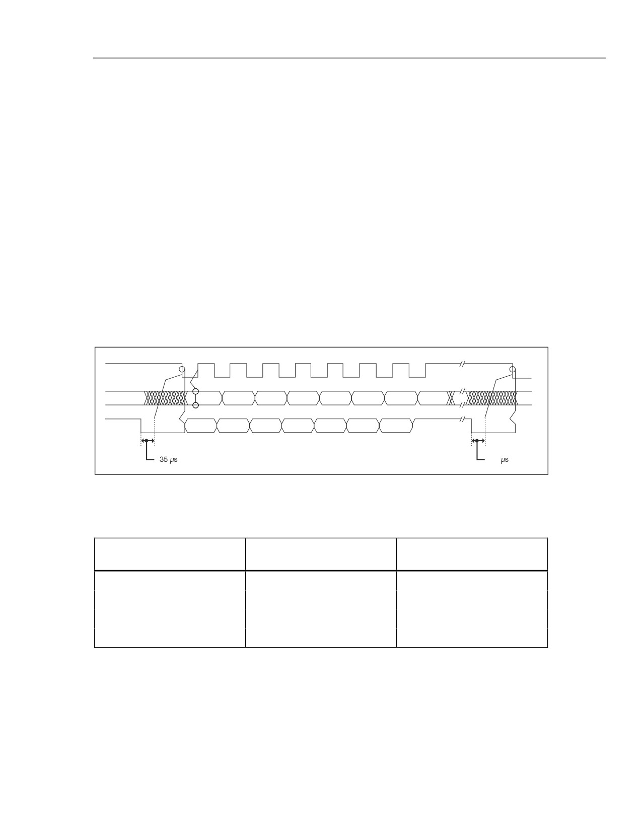
Theory of Operation
Detailed Circuit Description
2
kΩ (nominal) pull-down to the -30 V dc supply. These pull-downs are internal to the
Display Controller.
The output port, P63, of the Display Controller, is used as a grid control output for
GRID(10), of the vacuum-fluorescent display. A high voltage output, from P63, is
provided with a 10 kΩ resistor (A2R1), and PNP transistor (A2Q1) provide an active
driver to the +5 V dc supply and a passive 47 kΩ pull-down (A2R4) to -30 V dc.
The Display Controller drives the vacuum-fluorescent display in a multiplexed manner
by strobing each grid individually while the segment data for that display area is
presented on the anode outputs. Each grid is strobed for approximately 427
microseconds every 5.368 milliseconds, resulting in each grid on the display being
strobed about 170 times per second. The grid strobing sequence is from GRID(0) to
GRID(10), which results in right-to-left strobing of grid areas on the display. Figure 2-10
shows grid control signal timing.
The single grid strobing process involves turning off the previously enabled grid,
outputting the anode data for the next grid, and then enabling the next grid. This
procedure ensures that there is some time between grid strobes so that no shadowing
occurs on the display. Figure 2-11 describes the timing relationship between an
individual grid control signal and the anode control signals.
DSCLK
DISTX
BIT 7
BIT 6
BIT 5
BIT 4
BIT 3
BIT 2
BIT 1
BIT 0
DISRX
BIT 7
BIT 6
BIT 5
BIT 4
BIT 3
BIT 2
BIT 1
BIT 0
Clear to receive
Clear to receive
35
qb09.eps
Figure 2-9. Command Byte Transfer Waveforms
Table 2-6. Display Initialization Modes
A2TP4 Dtest*
A2TP5 LTE*
Power-Up Display
Initialization
1
1
All Segments OFF
1
0
All Segments ON (default)
0
1
Display Test Pattern #1
0
0
Display Test Pattern #2
2-23
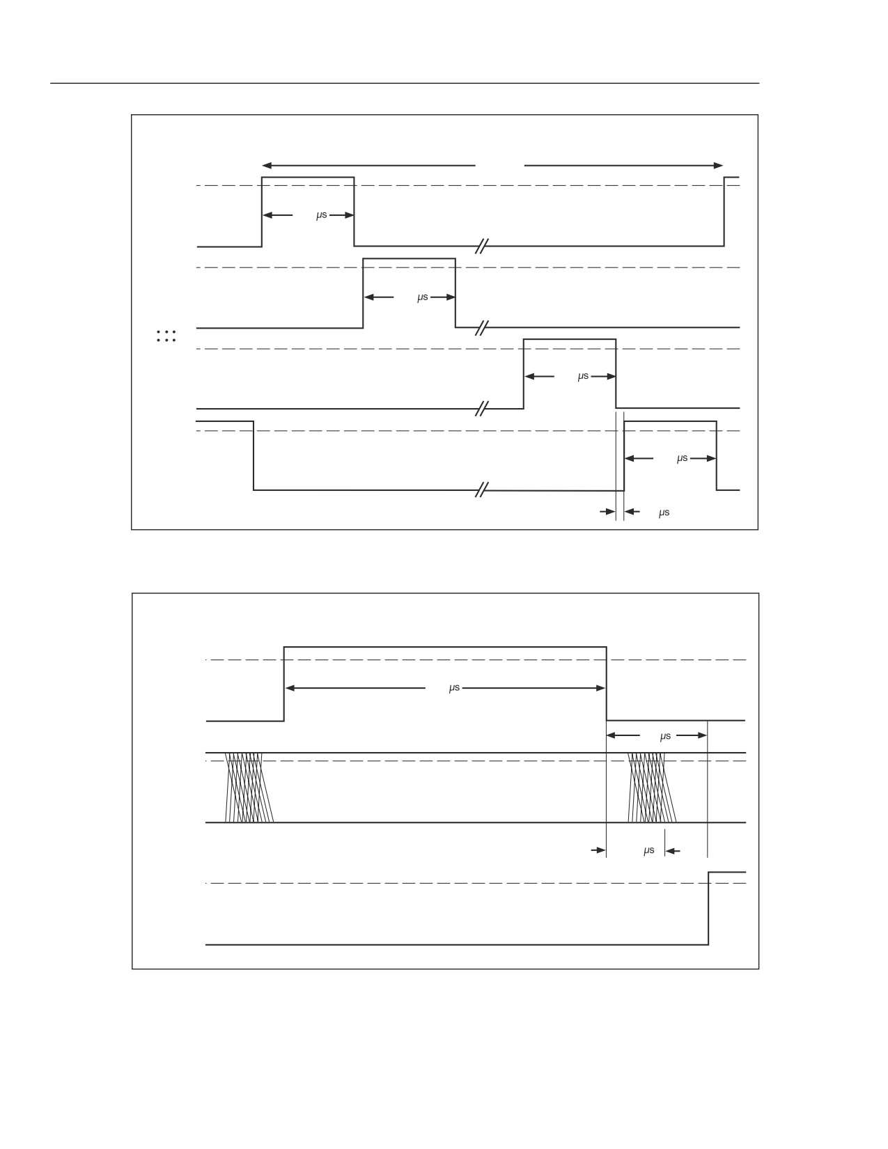
45
Service Manual
Grid Timing
5.368 ms
0V
Grid (0)
427
0V
Grid (1)
427
0V
Grid (9)
427
0V
Grid (10)
427
61
qb10f.eps
Figure 2-10. Grid Control Signal Timing
Grid/Anode Timing
5V
0V
Grid (X0)
427
-30V
61
5V
0V
Anode (14..0)
-30V
30.5
5V
0V
Grid (X-1)
-30V
qb11f.eps
Figure 2-11. Grid-Anode Timing Relationships
2-24
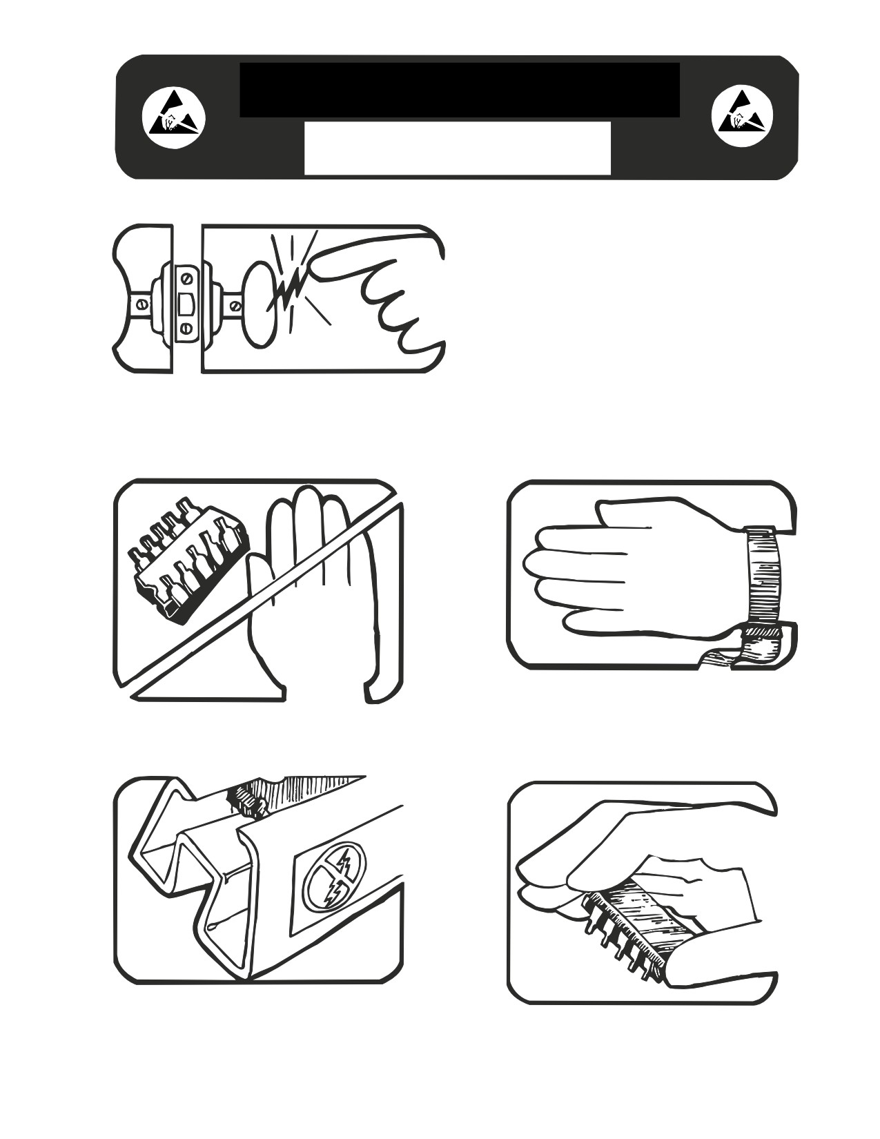
static awareness
A Message From
Fluke Corporation
Some semiconductors and custom IC's can be
damaged by electrostatic discharge during
handling. This notice explains how you can
minimize the chances of destroying such devices
by:
1. Knowing that there is a problem.
2. Leaning the guidelines for handling them.
3. Using the procedures, packaging, and
bench techniques that are recommended.
The following practices should be followed to minimize damage to S.S. (static sensitive) devices.
3. DISCHARGE PERSONAL STATIC BEFORE
HANDLING DEVICES. USE A HIGH RESIS-
1. MINIMIZE HANDLING
TANCE GROUNDING WRIST STRAP.
2. KEEP PARTS IN ORIGINAL CONTAINERS
4. HANDLE S.S. DEVICES BY THE BODY.
UNTIL READY FOR USE.
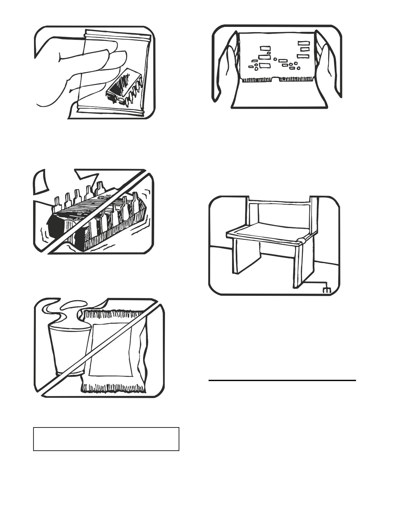
5. USE STATIC SHIELDING CONTAINERS FOR
8. WHEN REMOVING PLUG-IN ASSEMBLIES
HANDLING AND TRANSPORT.
HANDLE ONLY BY NON-CONDUCTIVE
EDGES AND NEVER TOUCH OPEN EDGE
CONNECTOR EXCEPT AT STATIC-FREE
WORK STATION. PLACING SHORTING
STRIPS ON EDGE CONNECTOR HELPS
PROTECT INSTALLED S.S. DEVICES.
6. DO NOT SLIDE S.S. DEVICES OVER
ANY SURFACE.
9. HANDLE S.S. DEVICES ONLY AT A
STATIC-FREE WORK STATION.
10. ONLY ANTI-STATIC TYPE SOLDER-
SUCKERS SHOULD BE USED.
11. ONLY GROUNDED-TIP SOLDERING
IRONS SHOULD BE USED.
7. AVOID PLASTIC,VINYL AND STYROFOAM®
IN WORK AREA.
PORTIONS REPRINTED
WITH PERMISSION FROM TEKTRONIX INC.
AND GERNER DYNAMICS, POMONA DIV.
® Dow Chemical
Chapter 3
General Maintenance
Title
Page
3-1.
Introduction
3-3
3-2.
Warranty Repairs and Shipping Information
3-3
3-3.
General Maintenance Information
3-3
3-4.
Required Equipment
3-3
3-5.
Power Requirements
3-3
3-6.
Static Safe Handling
3-3
3-7.
Cleaning
3-4
3-8.
Fuse Test and Replacement
3-4
3-9.
Line Fuse
3-4
3-10.
Current Input Fuses
3-4
3-11.
Testing Current Input Fuses
3-4
3-12.
Replacing the 500 mA and 440 mA Input Fuses (F1 and F5)
3-5
3-13.
Replacing the 10 A Input Jack Fuse (F2)
3-6
3-14.
Disassembly Procedures
3-7
3-15.
Remove the Meter Case
3-7
3-16.
Remove Handle and Mounting Brackets
3-7
3-17.
Remove the Front Panel Assembly
3-8
3-18.
Remove the Display PCA
3-8
3-19.
Remove the IEEE-488 Option
3-9
3-20.
Remove the Main PCA
3-9
3-21.
Remove the Analog Measurement Processor Shields
3-9
3-22.
Remove the Rms PCA
3-10
3-23.
Remove the Battery Option
3-10
3-24.
Disconnect Miscellaneous Chassis Components
3-10
3-25.
Assembly Procedures
3-10
3-26.
Install Miscellaneous Chassis Components
3-10
3-27.
Install the Battery Option
3-11
3-28.
Install the Rms PCA
3-11
3-29.
Install the Analog Measurement Processor Shields
3-11
3-30.
Install the Main PCA
3-11
3-31.
Install the IEEE-488 Option
3-12
3-32.
Assemble the Front Panel Assembly
3-12
3-33.
Install the Front Panel Assembly
3-15
3-34.
Install the Handle and Mounting Brackets
3-15
3-35.
Install the Meter Case
3-15
3-1
General Maintenance
Introduction
3
3-1.
Introduction
This provides handling, cleaning, fuse replacement, disassembly, and assembly
instructions.
3-2.
Warranty Repairs and Shipping Information
If your meter is still under warranty, see the warranty information at the front of this
manual for instructions on returning the unit. A list of Fluke telephone numbers and our
website address can be found at the end of the warranty information and in Chapter 6.
3-3.
General Maintenance Information
3-4.
Required Equipment
Equipment required for calibration, troubleshooting, and repair of the Fluke 45 is listed
in Table 4-4.
3-5.
Power Requirements
Warning
To avoid shock hazard, connect the meter power cord to a
power receptacle with earth ground.
If you have not already done so, plug the line cord into the connector on the rear of the
meter. The meter operates on any line voltage between 90 V ac and 264 V ac without
adjustment, and at any frequency between 45 and 440 Hz. However, the meter is only
warranted to meet published specifications at 50/60 Hz. The meter draws a maximum of
15 VA.
3-6.
Static Safe Handling
All integrated circuits, including surface mounted ICs, are susceptible to damage from
electrostatic discharge (ESD). Modern integrated circuit assemblies are more susceptible
to damage from ESD than ever before. Integrated circuits today can be built with circuit
lines less than one micron thick, allowing more than a million transistors on a 1/4-inch
square chip. These submicron structures are sensitive to static voltages under 100 volts.
This much voltage can be generated on a dry day by simply moving your arm. A person
can develop a charge of 2,000 volts by walking across a vinyl tile floor, and polyester
clothing can easily generate 5,000 to 15,000 volts during movement against the wearer.
These low voltage static problems are often undetected because a static charge must be
in the 30,000 to 40,000 volt range before a person will feel a shock.
Most electronic components manufactured today can be degraded or destroyed by ESD.
While protection networks are used in CMOS devices, they can only reduce, not
eliminate, component susceptibility to ESD.
ESD may not cause an immediate failure in a component; a delayed failure or
"wounding" effect is caused when the semiconductor’s insulation layers or junctions are
punctured. The static problem is thus complicated in that failure may occur anywhere
from two hours to six months after the initial damage.
3-3
45
Service Manual
Two failure modes are associated with ESD. First, a person who has acquired a static
charge can touch a component or assembly and cause a transient discharge to pass
through the device. The resulting current ruptures the junctions of a semiconductor. The
second failure mode does not require contact with another object. Simply exposing a
device to the electric field surrounding a charged object can destroy or degrade a
component. MOS devices can fail when exposed to static fields as low as 30 volts.
Observe the following rules for handling static-sensitive devices:
1. Handle all static-sensitive components at a static-safe work area.
Use grounded static control table mats on all repair benches, and always wear a
grounded wrist strap. Handle boards by their nonconductive edges only. Store
plastic, vinyl, and Styrofoam objects outside the work area.
2. Store and transport all static-sensitive components and assemblies in static shielding
bags or containers.
Static shielding bags and containers protect components and assemblies from direct
static discharge and external static fields. Store components in their original packages
until they are ready for use.
3-7.
Cleaning
Warning
To avoid electrical shock or damage to the meter, never allow
water inside the case. To avoid damaging the meter’s housing,
never apply solvents to the meter.
If the meter requires cleaning, wipe it down with a cloth that is lightly dampened with
water or a mild detergent. Do not use aromatic hydrocarbons, chlorinated solvents, or
methanol-based fluids when wiping the meter.
3-8.
Fuse Test and Replacement
3-9.
Line Fuse
The line fuse (a T 125 mA, 250 V, slow blow) is located on the rear panel. The fuse is in
series with the power supply. For replacement, unplug the line cord and remove the fuse
holder with fuse as shown in Figure 3-1. The meter is shipped with a replacement fuse.
3-10.
Current Input Fuses
The 100 mA and 10 A inputs are protected by replaceable fuses.
• The 100 mA input is protected by 2 fuses, F1 and F5. F1 is rated at F 500 mA, 250 V
(fast blow), 1500 A minimum breaking capacity, IEC-127 Sheet I and F5 is rated at
440 mA, 1000 V, 10,000 A minimum interrupt rating, (fast blow) fuse.
• The 10 A input is also protected by a fuse, F2, rated at F 11 A, 1000 V (fast blow),
17,000 A breaking capacity.
3-11.
Testing Current Input Fuses
Perform the following procedure to test these fuses:
1. Plug a test lead into the
input terminal, and power up the meter.
2. Press
to select the ohms function.
3-4
///////////////////////////////////////