Полупроводники. Каталог (2011 год) - часть 12


  Главная      Книги - Разные     Полупроводники. Каталог (2011 год)


поиск по сайту            правообладателям  


содержание      ..     10      11      12      13     ..


Полупроводники. Каталог (2011 год) - часть 12
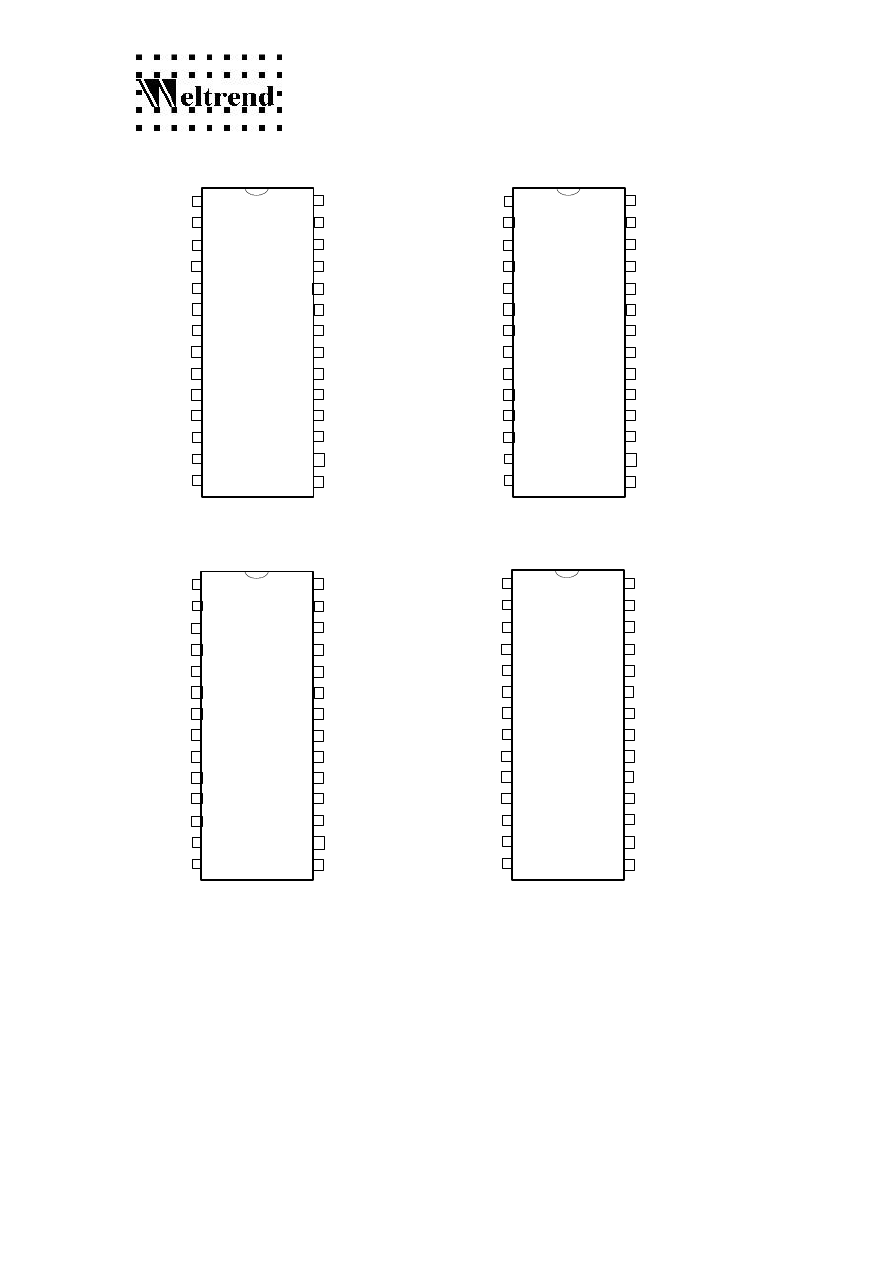


WT8045

Synchronous   Signal   Discriminator   and

Power Saving Detector for Green Monitor





Weltrend  Semiconductor,  Inc.

2F., No. 24, Industry E. 9th Rd.

Science-Based Industrial Park

Hsin-Chu, Taiwan, R.O.C.

Tel:  886-35-780241

Fax: 886-35-770419

25

1

2

3

4

5

6

7

8

9

10

11

12

13

14

15

16

OSCin

HSin

OSCout

VSin

H_out

V_out

VDD

WT8045N28P2

F43.5K

F36.2K

PM3

PM1

Vss

QHRC

640x400
(31.5K/37.5K)

640x480(31.5K)

800x600(48K)

17

18

19

20

21

22

800x600(37.5K)

800x600(35.2K)

1024x768(56.5K)

1024x768 (I)

F33K

640x480(37.5K)

1024x768 (NI)

28

27

26

25

24

23

QV128

QVRC

QH

F52K

PM2


1

2

3

4

5

6

7

8

9

10

11

12

13

14

15

16

OSCin

HSin

OSCout

VSin

H_out

V_out

VDD

WT8045N28P6

F43.5K

F36.2K

PM3

PM1

Vss

QHRC

640x400
(31.5K/37.5K)

640x480(31.5K)

800x600(48K)

17

18

19

20

21

22

800x600(37.5K)

800x600(35.2K)

1024x768(56.5K)

1024x768 (I)

F33K

640x480(37.5K)

1024x768 (NI)

28

27

26

25

24

23

QV1

QVRC

QH

F52K

PM2

1

2

3

4

5

6

7

8

9

10

11

12

13

14

15

16

OSCin

HSin

OSCout

VSin

H_out

V_out

VDD

WT8045N28P7

F43.5K

F36.2K

PM3

PM1 
+PM2

Vss

QHRC

640x400
(31.5K/37.5K)

640x480(31.5K)

800x600(48K)

17

18

19

20

21

22

800x600(37.5K)

800x600(35.2K)

1024x768(56.5K)

1024x768 (I)

F33K

640x480(37.5K)

1024x768 (NI)

28

27

26

25

24

23

QV128

QVRC

QH

F52K

Mute


1

2

3

4

5

6

7

8

9

10

11

12

13

14

15

16

OSCin

HSin

OSCout

VSin

H_out

V_out

VDD

WT8045N28P8

F43.5K

F36.2K

PM3

PM1 
+PM2

Vss

QHRC

640x400
(31.5K/37.5K)

640x480(31.5K)

800x600(48K)

17

18

19

20

21

22

800x600(37.5K)

800x600(35.2K)

1024x768(56.5K)

1024x768 (I)

F33K

640x480(37.5K)

1024x768 (NI)

28

27

26

25

24

23

QV1

QVRC

QH

F52K

Mute

Note: The Hout and Vout pin of  N28P2, N28P6, N28P7 and N28P8 are positive pulse.

REV. A

Information furnished by Analog Devices is believed to be accurate and
reliable. However, no responsibility is assumed by Analog Devices for its
use, nor for any infringements of patents or other rights of third parties
which may result from its use. No license is granted by implication or
otherwise under any patent or patent rights of Analog Devices.

a

Microprocessor

Supervisory Circuits

ADM690–ADM695

FEATURES
Superior Upgrade for MAX690–MAX695
Specified Over Temperature
Low Power Consumption (5 mW)
Precision Voltage Monitor
Reset Assertion Down to 1 V V

CC

Low Switch On-Resistance 1.5 

V

 Normal,

20 

V

 in Backup

High Current Drive (100 mA)
Watchdog Timer—100 ms, 1.6 s, or Adjustable
600 nA Standby Current
Automatic Battery Backup Power Switching
Extremely Fast Gating of Chip Enable Signals (5 ns)
Voltage Monitor for Power Fail

APPLICATIONS
Microprocessor Systems
Computers
Controllers
Intelligent Instruments
Automotive Systems

GENERAL DESCRIPTION
The ADM690–ADM695 family of supervisory circuits offers
complete single chip solutions for power supply monitoring and
battery control functions in microprocessor systems. These
functions include 

µ

P reset, backup battery switchover, watchdog

timer, CMOS RAM write protection, and power failure warn-
ing. The complete family provides a variety of configurations to
satisfy most microprocessor system requirements.

The ADM690, ADM692 and ADM694 are available in 8-pin
DIP packages and provide:

1. Power-on reset output during power-up, power-down and

brownout conditions. The 

RESET

 output remains opera-

tional with V

CC

 as low as 1 V.

2. Battery backup switching for CMOS RAM, CMOS

microprocessor or other low power logic.

3. A reset pulse if the optional watchdog timer has not been

toggled within a specified time.

4. A 1.3 V threshold detector for power fail warning, low battery

detection, or to monitor a power supply other than +5 V.

The ADM691, ADM693 and ADM695 are available in 16-pin
DIP and small outline packages and provide three additional
functions.

1. Write protection of CMOS RAM or EEPROM.

2. Adjustable reset and watchdog timeout periods.

3. Separate watchdog timeout, backup battery switchover, and

low V

CC

 status outputs.

The ADM690–ADM695 family is fabricated using an advanced
epitaxial CMOS process combining low power consumption
(5 mW), extremely fast Chip Enable gating (5 ns) and high reli-
ability. 

RESET

 assertion is guaranteed with V

CC

 as low as 1 V.

In addition, the power switching circuitry is designed for mini-
mal voltage drop thereby permitting increased output current
drive of up to 100 mA without the need for an external pass
transistor.

FUNCTIONAL BLOCK DIAGRAMS

4.65V

1

WATCHDOG

TRANSITION DETECTOR

1.3V

ADM691
ADM693
ADM695

V

OUT

V

BATT

V

CC

WATCHDOG

INPUT (WDI)

POWER FAIL

INPUT (PFI)

1

VOLTAGE DETECTOR = 4.65V (ADM691, ADM695)

                                            4.40V (ADM693)

POWER FAIL
OUTPUT (PFO)

RESET

WATCHDOG

TIMER

RESET &

WATCHDOG

TIMEBASE

RESET

GENERATOR

BATT ON

OSC IN

OSC SEL

WATCHDOG
OUTPUT (WDO)

RESET

LOW LINE

CE

OUT

CE

IN

4.65V

1

RESET

GENERATOR

2

WATCHDOG

TRANSITION DETECTOR

(1.6s)

1.3V

ADM690
ADM692
ADM694

V

OUT

V

BATT

V

CC

WATCHDOG

INPUT (WDI)

POWER FAIL

INPUT (PFI)

1

VOLTAGE DETECTOR = 4.65V (ADM690, ADM694)

                                            4.40V (ADM692)

2

RESET PULSE WIDTH = 50ms (ADM690, ADM692)

                                           200ms (ADM694)

POWER FAIL
OUTPUT (PFO)

RESET

One Technology Way, P.O. Box 9106, Norwood, MA 02062-9106,  U.S.A.
Tel: 617/329-4700

Fax: 617/326-8703

ADM690–ADM695–SPECIFICATIONS

Parameter

Min

Typ

Max

Units

Test Conditions/Comments

BATTERY BACKUP SWITCHING

V

CC

 Operating Voltage Range

ADM690, ADM691, ADM694, ADM695

4.75

5.5

V

ADM692, ADM693

4.5

5.5

V

V

BATT

 Operating Voltage Range

ADM690, ADM691, ADM694, ADM695

2.0

4.25

V

ADM692, ADM693

2.0

4.0

V

V

OUT

 Output Voltage

V

CC

  – 0.05

V

CC

 – 0.025

V

I

OUT

 = 1 mA

V

CC

 – 0.5

V

CC

 – 0.25

V

I

OUT


 100 mA

V

OUT

 in Battery Backup Mode

V

BATT 

– 0.05 V

BATT

 – 0.02

V

I

OUT

 = 250 

µ

A, V

CC

 < V

BATT

 – 0.2 V

Supply Current (Excludes I

OUT

)

1

1.95

mA

I

OUT

 = 100 mA

Supply Current in Battery Backup Mode

0.6

1

µ

A

V

CC

 = 0 V, V

BATT

 = 2.8 V

Battery Standby Current

5.5 V > V

CC

 > V

BATT

 + 0.2 V

(+ = Discharge, – = Charge)

–0.1

+0.02

µ

A

T

= +25

°

C

–1.0

+0.02

µ

A

Battery Switchover Threshold

70

mV

Power Up

V

CC

 – V

BATT

50

mV

Power Down

Battery Switchover Hysteresis

20

mV

BATT ON Output Voltage

0.3

V

I

SINK

 = 3.2 mA

BATT ON Output Short Circuit Current

35

mA

BATT ON = V

OUT

 = 4.5 V Sink Current

0.5

1

25

µ

A

BATT ON = 0 V Source Current

RESET AND WATCHDOG TIMER

Reset Voltage Threshold

ADM690, ADM691, ADM694, ADM695

4.5

4.65

4.73

V

ADM692, ADM693

4.25

4.4

4.48

V

Reset Threshold Hysteresis

40

mV

Reset Timeout Delay

ADM690, ADM691, ADM692, ADM693

35

50

70

ms

OSC SEL = HIGH, V

CC

 = 5 V, T

A

 = +25

°

C

ADM694, ADM695

140

200

280

ms

OSC SEL = HIGH, V

CC

 = 5 V, T

A

 = +25

°

C

Watchdog Timeout Period, Internal Oscillator

1.0

1.6

2.25

s

Long Period, V

CC

 = 5 V, T

A

 = +25

°

C

70

100

140

ms

Short Period, V

CC

 = 5 V, T

A

 = +25

°

C

Watchdog Timeout Period, External Clock

3840

4097

Cycles

Long Period

768

1025

Cycles

Short Period

Minimum WDI Input Pulse Width

50

ns

V

IL

 = 0.4, V

IH

 = 3.5 V

RESET

 Output Voltage @ V

CC

 = +1 V

4

200

mV

I

SINK

 = 10 

µ

A, V

CC

 = 1 V

RESET

LOW


LINE

 Output Voltage

0.4

V

I

SINK

 = 1.6 mA, V

CC

 = 4.25 V

3.5

V

I

SOURCE

 = 1 

µ

A, V

CC

 = 5 V

RESET

WDO

 Output Voltage

0.4

V

I

SINK

 = 1.6 mA, V

CC

 = 5 V

3.5

V

I

SOURCE

 = 1 

µ

A, V

CC

 = 4.25 V

Output Short Circuit Source Current

1

3

25

µ

A

Output Short Circuit Sink Current

25

mA

WDI Input Threshold

V

CC

 = 5 V

1

Logic Low

0.8

V

Logic High

3.5

V

WDI Input Current

20

50

µ

A

WDI = V

OUT

, T

A

 = +25

°

C

–50

–15

µ

A

WDI = 0 V, T

A

 = +25

°

C

POWER FAIL DETECTOR

PFI Input Threshold

1.25

1.3

1.35

V

V

CC

 = +5 V

PFI Input Current

–25

±

0.01

+25

nA

PFO

 Output Voltage

0.4

V

I

SINK

 = 3.2 mA

3.5

V

I

SOURCE

 = 1 

µ

A

PFO

 Short Circuit Source Current

1

3

25

µ

A

PFI = Low, 

PFO

 = 0 V

PFO

 Short Circuit Sink Current

25

mA

PFI = High, 

PFO

 = V

OUT

CHIP ENABLE GATING

CE

IN

 Threshold

0.8

V

V

IL

3.0

V

V

IH

CE

IN

 Pull-Up Current

3

µ

A

CE

OUT

 Output Voltage

0.4

V

I

SINK

 = 3.2 mA

V

OUT

 – 1.5

V

I

SOURCE

 = 3.0 mA

V

OUT

 – 0.05

V

I

SOURCE

 = 1 

µ

A, V

CC

 = 0 V

CE

 Propagation Delay

5

9

ns

REV. A

(V

CC

 = Full Operating Range, V

BATT

 = +2.8 V, T

A

 = T

MIN

 to

T

MAX

 unless otherwise noted)

–2–

Parameter

Min

Typ

Max

Units

Test Conditions/Comments

OSCILLATOR

OSC IN Input Current

±

2

µ

A

OSC SEL Input Pull-Up Current

5

µ

A

OSC IN Frequency Range

0

250

kHz

 OSC SEL = 0 V

OSC IN Frequency with External Capacitor

4

kHz

 OSC SEL = 0 V, C

OSC

 = 47 pF

NOTE

1

WDI is a three level input which is internally biased to 38% of V

CC

 and has an input impedance of approximately 125 k

.

Specifications subject to change without notice.

ADM690–ADM695

REV. A

–3–

ABSOLUTE MAXIMUM RATINGS*

(T

A

 = +25

°

C unless otherwise noted)

V

CC

 . . . . . . . . . . . . . . . . . . . . . . . . . . . . . . . . . . –0.3 V to +6 V

V

BATT

 . . . . . . . . . . . . . . . . . . . . . . . . . . . . . . . . –0.3 V to +6 V

All Other Inputs  . . . . . . . . . . . . . . . . . . –0.3 V to V

OUT

 + 0.5 V

Input Current

V

CC

 . . . . . . . . . . . . . . . . . . . . . . . . . . . . . . . . . . . . . 200 mA

V

BATT

 . . . . . . . . . . . . . . . . . . . . . . . . . . . . . . . . . . . . 50 mA

GND  . . . . . . . . . . . . . . . . . . . . . . . . . . . . . . . . . . . . . 20 mA

Digital Output Current  . . . . . . . . . . . . . . . . . . . . . . . . . 20 mA
Power Dissipation, N-8 DIP  . . . . . . . . . . . . . . . . . . . . 400 mW

θ

JA

 Thermal Impedance  . . . . . . . . . . . . . . . . . . . . . 120

°

C/W

Power Dissipation, Q-8 DIP  . . . . . . . . . . . . . . . . . . . . 500 mW

θ

JA

 Thermal Impedance  . . . . . . . . . . . . . . . . . . . . . 125

°

C/W

Power Dissipation, N-16 DIP  . . . . . . . . . . . . . . . . . . . 600 mW

θ

JA

 Thermal Impedance  . . . . . . . . . . . . . . . . . . . . . 135

°

C/W

Power Dissipation, Q-16 DIP  . . . . . . . . . . . . . . . . . . . 600 mW

θ

JA

 Thermal Impedance  . . . . . . . . . . . . . . . . . . . . . 100

°

C/W

Power Dissipation, R-16 SOIC  . . . . . . . . . . . . . . . . . . 600 mW

θ

JA

 Thermal Impedance  . . . . . . . . . . . . . . . . . . . . . 110

°

C/W

Operating Temperature Range

Industrial (A Version)  . . . . . . . . . . . . . . . . . –40

°

C to +85

°

C

Extended (S Version)  . . . . . . . . . . . . . . . . . –55

°

C to +125

°

C

Lead Temperature (Soldering, 10 secs)  . . . . . . . . . . . . +300

°

C

Vapor Phase (60 secs)  . . . . . . . . . . . . . . . . . . . . . . . +215

°

C

Infrared (15 secs)  . . . . . . . . . . . . . . . . . . . . . . . . . . . +220

°

C

Storage Temperature Range  . . . . . . . . . . . . . –65

°

C to +150

°

C

*Stresses above those listed under “Absolute Maximum Ratings” may cause

permanent damage to the device. This is a stress rating only and functional
operation of the device at these or any other conditions above those listed in the
operational sections of this specification is not implied. Exposure to absolute
maximum ratings for extended periods of time may affect device reliability.

ORDERING GUIDE

Model

Temperature Range

Package Option

ADM690AN

–40

°

C to +85

°

C

N-8

ADM690AQ

–40

°

C to +85

°

C

Q-8

ADM690SQ

–55

°

C to +125

°

C

Q-8

ADM691AN

–40

°

C to +85

°

C

N-16

ADM691AR

–40

°

C to +85

°

C

R-16

ADM691AQ

–40

°

C to +85

°

C

Q-16

ADM691SQ

–55

°

C to +125

°

C

Q-16

ADM692AN

–40

°

C to +85

°

C

N-8

ADM692AQ

–40

°

C to +85

°

C

Q-8

ADM692SQ

–55

°

C to +125

°

C

Q-8

ADM693AN

–40

°

C to +85

°

C

N-16

ADM693AR

–40

°

C to +85

°

C

R-16

ADM693AQ

–40

°

C to +85

°

C

Q-16

ADM693SQ

–55

°

C to +125

°

C

Q-16

ADM694AN

–40

°

C to +85

°

C

N-8

ADM694AQ

–40

°

C to +85

°

C

Q-8

ADM694SQ

–55

°

C to +125

°

C

Q-8

ADM695AN

–40

°

C to +85

°

C

N-16

ADM695AR

–40

°

C to +85

°

C

R-16

ADM695AQ

–40

°

C to +85

°

C

Q-16

ADM695SQ

–55

°

C to +125

°

C

Q-16

WARNING!

ESD SENSITIVE DEVICE

CAUTION
ESD (electrostatic discharge) sensitive device. Electrostatic charges as high as 4000 V readily
accumulate on the human body and test equipment and can discharge without detection.
Although the ADM690–ADM695 features proprietary ESD protection circuitry, permanent
damage may occur on devices subjected to high energy electrostatic discharges. Therefore,
proper ESD precautions are recommended to avoid performance degradation or loss of
functionality.

ADM690–ADM695

REV. A

–4–

PIN FUNCTION DESCRIPTION

Mnemonic

Function

V

CC

Power Supply Input: +5 V Nominal.

V

BATT

Backup Battery Input. Connect to Ground if a backup battery is not used.

V

OUT

Output Voltage, V

CC

 or V

BATT

 is internally switched to V

OUT

 depending on which is at the highest potential. V

OUT

can supply up to 100 mA to power CMOS RAM. Connect V

OUT

 to V

CC

 if V

OUT

 and V

BATT

 are not used.

GND

0 V. Ground reference for all signals.

RESET

Logic Output. 

RESET

 goes low if

1. V

CC

 falls below the Reset Threshold

2. V

CC

 falls below V

BATT

3. The watchdog timer is not serviced within its timeout period.

The reset threshold is typically 4.65 V for the ADM690/ADM691/ADM694/ADM695 and 4.4 V for the ADM692 and
ADM693. 

RESET

 remains low for 50 ms (ADM690/ADM691/ADM692/ADM693) or 200 ms (ADM694/ADM695)

after V

CC

 returns above the threshold. 

RESET

 also goes low for 50 (200) ms if the watchdog timer is enabled but not

serviced within its timeout period. The 

RESET

 pulse width can be adjusted on the ADM691/ADM693/ADM695 as

shown in Table I. The 

RESET

 output has an internal 3 

µ

A pull up, and can either connect to an open collector

Reset bus or directly drive a CMOS gate without an external pull-up resistor.

WDI

Watchdog Input. WDI is a three level input. If WDI remains either high or low for longer than the watchdog timeout
period, 

RESET

 pulses low and WDO goes low. The timer resets with each transition on the WDI line. The watchdog

timer may be disabled if WDI is left floating or is driven to midsupply.

PFI

Power Fail Input. PFI is the noninverting input to the Power Fail Comparator when PFI is less than 1.3 V, 

PFO

goes low. Connect PFI to GND or V

OUT

 when not used.

PFO

Power Fail Output. 

PFO

 is the output of the Power Fail Comparator. It goes low when PFI is less than 1.3 V. The

comparator is turned off and 

PFO

 goes low when V

CC

 is below V

BATT

.

CE

IN

Logic Input. The input to the 

CE

 gating circuit. Connect to GND or V

OUT

 if not used.

CE

OUT

Logic Output. 

CE

OUT

 is a gated version of the 

CE

IN

 signal. 

CE

OUT

 tracks 

CE

IN

 when V

CC

 is above the reset

threshold. If V

CC

 is below the reset threshold, 

CE

OUT

 is forced high. See Figures 5 and 6.

BATT ON

Logic Output. BATT ON goes high when V

OUT

 is internally switched to the V

BATT

 input. It goes low when V

OUT

is internally switched to V

CC

. The output typically sinks 35 mA and can directly drive the base of an external

PNP transistor to increase the output current above the 100 mA rating of V

OUT

.

LOW LINE

Logic Output. 

LOW LINE

 goes low when V

CC

 falls below the reset threshold. It returns high as soon as V

CC

 rises

above the reset threshold.

RESET

Logic Output. RESET is an active high output. It is the inverse of 

RESET

.

OSC SEL

Logic Oscillator Select Input. When OSC SEL is unconnected (floating) or driven high, the internal oscillator sets
the reset active time and watchdog timeout period. When OSC SEL is low, the external oscillator input, OSC IN,
is enabled. OSC SEL has a 3 

µ

A internal pull up, (see Table I).

OSC IN

Oscillator Logic Input. With OSC SEL low, OSC IN can be driven by an external clock signal or an external
capacitor can be connected between OSC IN and GND. This sets both the reset active pulse timing and the watch-
dog timeout period (see Table I and Figure 4). With OSC SEL high or floating, the internal oscillator is enabled
and the reset active time is fixed at 50 ms typ. (ADM691/ADM693) or 200 ms typ (ADM695). In this mode the
OSC IN pin selects between fast (100 ms) and slow (1.6 s) watchdog timeout periods. In both modes, the timeout
period immediately after a reset is 1.6 s typical.

WDO

Logic Output. The Watchdog Output, 

WDO

, goes low if WDI remains either high or low for longer than the

watchdog timeout period. 

WDO

 is set high by the next transition at WDI. If WDI is unconnected or at midsupply,

the watchdog timer is disabled and 

WDO

 remains high. 

WDO

 also goes high when 

LOW LINE

 goes low.

ADM690–ADM695

REV. A

–5–

PIN CONFIGURATIONS

PRODUCT SELECTION GUIDE

Part

Nominal Reset

Nominal V

CC

Nominal Watchdog

Battery Backup

Base Drive

Chip Enable

Number

Time

Reset Threshold

Timeout Period

Switching

Ext PNP

Signals

ADM690

50 ms

4.65 V

1.6 s

Yes

No

No

ADM691

50 ms or ADJ

4.65 V

100 ms, 1.6 s, ADJ

Yes

Yes

Yes

ADM692

50 ms

4.4 V

1.6 s

Yes

No

No

ADM693

50 ms or ADJ

4.4 V

100 ms, 1.6 s, ADJ

Yes

Yes

Yes

ADM694

200 ms

4.65 V

1.6 s

Yes

No

No

ADM695

200 ms or ADJ

4.65 V

100 ms, 1.6 s, ADJ

Yes

Yes

Yes

CIRCUIT INFORMATION
Battery Switchover Section
The battery switchover circuit compares V

CC

 to the V

BATT

input, and connects V

OUT

 to whichever is higher. Switchover

occurs when V

CC

 is 50 mV higher than V

BATT

 as V

CC

 falls, and

when V

CC

 is 70 mV greater than V

BATT

 as V

CC

 rises. This

20 mV of hysteresis prevents repeated rapid switching if V

CC

falls very slowly or remains nearly equal to the battery voltage.

Figure 1. Battery Switchover Schematic

During normal operation with V

CC

 higher than V

BATT

, V

CC

 is in-

ternally switched to V

OUT 

via an internal PMOS transistor

switch. This switch has a typical on-resistance of 1.5 

 and can

supply up to 100 mA at the V

OUT

 terminal. V

OUT

 is normally

used to drive a RAM memory bank which may require instanta-
neous currents of greater than 100 mA. If this is the case then a
bypass capacitor should be connected to V

OUT

. The capacitor

will provide the peak current transients to the RAM. A capaci-
tance value of 0.1

µ

F or greater may be used.

If the continuous output current requirement at V

OUT

 exceeds

100 mA or if a lower V

CC

–V

OUT

 voltage differential is desired,

an external PNP pass transistor may be connected in parallel
with the internal transistor. The BATT ON output (ADM691/
ADM693/ADM695) can directly drive the base of the external
transistor.

A 20 

 MOSFET switch connects the V

BATT

 input to V

OUT

during battery backup. This MOSFET has very low input-to-
output differential (dropout voltage) at the low current levels
required for battery back up of CMOS RAM or other low
power CMOS circuitry. The supply current in battery back up
is typically 0.6 

µ

A.

The ADM690/ADM691/ADM694/ADM695 operates with
battery voltages from 2.0 V to 4.25 V and the ADM692/ADM693
operates with battery voltages from 2.0 V to 4.0 V. High value
capacitors, either standard electrolytic or the farad size double
layer capacitors, can also be used for short-term memory back
up. A small charging current of typically 10 nA (0.1 

µ

A max)

flows out of the V

BATT

 terminal. This current is useful for

maintaining rechargeable batteries in a fully charged condition.
This extends the life of the back up battery by compensating
for its self discharge current. Also note that this current poses
no problem when lithium batteries are used for back up since
the maximum charging current (0.1 

µ

A) is safe for even the

smallest lithium cells.

If the battery-switchover section is not used, V

BATT

 should be

connected to GND and V

OUT

 should be connected to V

CC

.

1

2

3

4

5

6

7

8

16

15

14

13

12

11

10

9

TOP VIEW

(Not to Scale)

ADM691
ADM693
ADM695

GND

V

BATT

V

OUT

PFI

PFO

WDO

V

CC

RESET

BATT ON

LOW LINE

OSC IN

OSC SEL

RESET

CE

IN

CE

OUT

WDI

GND

V

BATT

V

OUT

PFI

PFO

WDI

RESET

V

CC

1

2

3

4

8

7

6

5

TOP VIEW

(Not to Scale)

ADM690
ADM692
ADM694

ADM690–ADM695

REV. A

–6–

POWER FAIL 

RESET

 OUTPUT

RESET

 is an active low output which provides a 

RESET

 signal

to the Microprocessor whenever V

CC

 is at an invalid level. When

V

CC

 falls below the reset threshold, the 

RESET

 output is forced

low. The nominal reset voltage threshold is 4.65 V (ADM690/
ADM691/ADM694/ADM695) or 4.4 V (ADM692/ADM693).

t

1

t

= RESET TIME.

V1 = RESET VOLTAGE THRESHOLD LOW

V2 = RESET VOLTAGE THRESHOLD HIGH

HYSTERESIS = V2–V1

V2

V2

V1

V1

t

1

V

CC

LOW LINE

RESET

Figure 2. Power Fail Reset Timing

On power-up 

RESET

 will remain low for 50 ms (200 ms for

ADM694 and ADM695) after V

CC

 rises above the appropriate

reset threshold. This allows time for the power supply and mi-
croprocessor to stabilize. On power-down, the 

RESET

 output

remains low with V

CC

 as low as 1 V. This ensures that the

microprocessor is held in a stable shutdown condition.

This 

RESET

 active time is adjustable on the ADM691/ADM693/

ADM695 by using an external oscillator or by connecting an
external capacitor to the OSC IN pin. Refer to Table I and
Figure 4.

The guaranteed minimum and maximum thresholds of the
ADM690/ADM691/ADM694/ADM695 are 4.5 V and 4.73 V,
while the guaranteed thresholds of the ADM692/ADM693 are
4.25 V and 4.48 V. The ADM690/ADM691/ADM694/ADM695
is, therefore, compatible with 5 V supplies with a +10%, –5%
tolerance while the ADM692/ADM693 is compatible with 5 V

±

 10% supplies. The reset threshold comparator has approxi-

mately 50 mV of hysteresis. The response time of the reset volt-
age comparator is less than 1 

µ

s. If glitches are present on the

V

CC

 line which could cause spurious reset pulses, then V

CC

should be decoupled close to the device.

In addition to 

RESET

 the ADM691/ADM693/ADM695 con-

tain an active high 

RESET

 output. This is the complement of

RESET

 and is intended for processors requiring an active high

RESET signal.

Watchdog Timer 

RESET

The watchdog timer circuit monitors the activity of the micro-
processor in order to check that it is not stalled in an indefinite
loop. An output line on the processor is used to toggle the
Watchdog Input (WDI) line. If this line is not toggled within the
selected timeout period, a 

RESET

 pulse is generated. The

nominal watchdog timeout period is preset at 1.6 seconds on the
ADM690/ADM692/ADM694. The ADM691/ADM693/ADM695
may be configured for either a fixed “short” 100 ms or a “long”
1.6 second timeout period or for an adjustable timeout period.
If the “short” period is selected, some systems may be unable to
service the watchdog timer immediately after a reset, so the
ADM691/ADM693/ADM695 automatically selects the “long”
timeout period directly after a reset is issued. The watchdog
timer is restarted at the end of reset, whether the reset was
caused by lack of activity on WDI or by V

CC

 falling below the

reset threshold.

The normal (short) timeout period becomes effective following
the first transition of WDI after 

RESET

 has gone inactive. The

watchdog timeout period restarts with each transition on the
WDI pin. To ensure that the watchdog timer does not time out,
either a high-to-low or low-to-high transition on the WDI pin
must occur at or less than the minimum timeout period. If WDI
remains permanently either high or low, reset pulses will be
issued after each “long” timeout period (1.6 s). The watchdog
monitor can be deactivated by floating the Watchdog Input
(WDI) or by connecting it to midsupply.

t

2

RESET

WDO

WDI

t

1

 = RESET TIME.

t

2

 = NORMAL (SHORT) WATCHDOG TIMEOUT PERIOD.

t

= WATCHDOG TIMEOUT PERIOD IMMEDIATELY FOLLOWING A RESET.

t

1

t

1

t

1

t

3

Figure 3. Watchdog Timeout Period and Reset Active
Time

ADM690–ADM695

REV. A

–7–

Table I. ADM691, ADM693, ADM695 Reset Pulse Width and Watchdog Timeout Selections

     Watchdog Timeout Period

          Reset Active Period

Immediately

OSC SEL

OSC IN

Normal

After Reset

ADM691/ADM693

ADM695

Low

External Clock Input

1024 CLKS

4096 CLKS

512 CLKS

2048 CLKS

Low

External Capacitor

260 ms 

× 

 C/47 pF

1.04 s 

×

 C/47 pF

130 ms 

× 

C/47 pF

520 ms 

× 

 C/47 pF

Floating or High

Low

100 ms

1.6 s

50 ms

200 ms

Floating or High

Floating or High

1.6 s

1.6 s

50 ms

200 ms

NOTE
With the OSC SEL pin low, OSC IN can be driven by an external clock signal, or an external capacitor can be connected between OSC IN and GND. The nominal
internal oscillator frequency is 10.24 kHz. The nominal oscillator frequency with external capacitor is: F

OSC

 (Hz) = 184,001/C (pF).

The watchdog timeout period is fixed at 1.6 seconds, and the
reset pulse width is fixed at 50 ms on the ADM690/ADM692.
On the ADM694 the watchdog timeout period is also 1.6 sec-
onds but the reset pulse width is fixed at 200 ms. The ADM691/
ADM693/ADM695 allow these times to be adjusted as shown
in Table I. Figure 4 shows the various oscillator configurations
which can be used to adjust the reset pulse width and watchdog
timeout period.

The internal oscillator is enabled when OSC SEL is high or
floating. In this mode, OSC IN selects between the 1.6 second
and 100 ms watchdog timeout periods. With OSC IN connected
high or floating, the 1.6 second timeout period is selected; while
with it connected low, the 100 ms timeout period is selected. In
either case, immediately after a reset, the timeout period is 1.6
seconds. This gives the microprocessor time to reinitialize the
system. If OSC IN is low, then the 100 ms watchdog period be-
comes effective after the first transition of WDI. The software
should be written such that the I/O port driving WDI is left in
its power-up reset state until the initialization routines are com-
pleted and the microprocessor is able to toggle WDI at the mini-
mum watchdog timeout period of 70 ms.

Watchdog Output (WDO)
The Watchdog Output 

WDO

 (ADM691/ADM693/ADM695)

provides a status output which goes low if the watchdog timer
“times out” and remains low until set high by the next transition
on the Watchdog Input. 

WDO

 is also set high when V

CC

 goes

below the reset threshold.

OSC IN

OSC SEL

ADM691
ADM693
ADM695

CLOCK

0 TO 250kHz

8

7

Figure 4a. External Clock Source

OSC IN

OSC SEL

ADM691
ADM693
ADM695

8

7

C

OSC

Figure 4b. External Capacitor

OSC IN

OSC SEL

ADM691
ADM693
ADM695

8

7

NC

NC

Figure 4c. Internal Oscillator (1.6 Second Watchdog)

OSC IN

OSC SEL

ADM691
ADM693
ADM695

8

7

NC

Figure 4d. Internal Oscillator (100 ms Watchdog)

ADM690–ADM695

REV. A

–8–

CE

 Gating and RAM Write Protection (ADM691/ADM693/

ADM695)
The ADM691/ADM693/ADM695 products include memory
protection circuitry which ensures the integrity of data in mem-
ory by preventing write operations when V

CC

 is at an invalid

level. There are two additional pins, 

CE

IN

 and 

CE

OUT

, which

may be used to control the Chip Enable or Write inputs of
CMOS RAM. When V

CC

 is present, 

CE

OUT

 is a buffered replica

of 

CE

IN

, with a 5 ns propagation delay. When V

CC

 falls below

the reset voltage threshold or V

BATT

, an internal gate forces

CE

OUT

 high, independent of 

CE

IN

.

CE

OUT

 typically drives the 

CE

CS

, or write input of battery

backed up CMOS RAM. This ensures the integrity of the data
in memory by preventing write operations when V

CC

 is at an in-

valid level. Similar protection of EEPROMs can be achieved by
using the 

CE

OUT

 to drive the store or write inputs.

If the 5 ns typical propagation delay of 

CE

OUT

 is excessive, con-

nect 

CE

IN

 to GND and use the resulting 

CE

OUT

 to control a

high speed external logic gate.

ADM69x

CE

OUT

CE

IN

V

CC

 LOW = 0

V

CC

 OK = 1

Figure 5. Chip Enable Gating

Power Fail Warning Comparator
An additional comparator is provided for early warning of failure
in the microprocessor’s power supply. The Power Fail Input
(PFI) is compared to an internal +1.3 V reference. The Power
Fail Output (

PFO

) goes low when the voltage at PFI is less than

1.3 V. Typically PFI is driven by an external voltage divider
which senses either the unregulated dc input to the system’s 5 V
regulator or the regulated 5 V output. The voltage divider ratio
can be chosen such that the voltage at PFI falls below 1.3 V sev-
eral milliseconds before the +5 V power supply falls below the
reset threshold. 

PFO

 is normally used to interrupt the micropro-

cessor so that data can be stored in RAM and the shut down
procedure executed before power is lost

ADM69x

POWER

FAIL

INPUT

R

2

INPUT

POWER

1.3V

PFO

POWER
FAIL
OUTPUT

R

1

Figure 7. Power Fail Comparator

Table II. Input and Output Status In Battery Backup Mode

Signal

Status

V

OUT

V

OUT

 is connected to V

BATT

 via an internal

PMOS switch.

RESET

Logic low.

RESET

Logic high. The open circuit output voltage is
equal to V

OUT

.

LOW LINE

Logic low.

BATT ON

Logic high. The open circuit voltage is equal to
V

OUT.


WDI

WDI is ignored. It is internally disconnected
from the internal pull-up resistor and does not
source or sink current as long as its input voltage
is between GND and V

OUT

. The input voltage

does not affect supply current.

WDO

Logic high. The open circuit voltage is equal
to V

OUT

.

PFI

The Power Fail Comparator is turned off and
has no effect on the Power Fail Output.

PFO

Logic low.

CE

IN

CE

IN

 is ignored. It is internally disconnected

from its internal pull-up and does not source or
sink current as long as its input voltage is
between GND and V

OUT

. The input voltage

does not affect supply current.

CE

OUT

Logic high. The open circuit voltage is equal to
V

OUT

.

OSC IN

OSC IN is ignored.

OSC SEL

OSC SEL is ignored.

t

1

t

= RESET TIME.

V1 = RESET VOLTAGE THRESHOLD LOW

V2 = RESET VOLTAGE THRESHOLD HIGH

HYSTERESIS = V2–V1

V2

V2

V1

V1

t

1

V

CC

LOW LINE

RESET

CE

IN

CE

OUT

Figure 6. Chip Enable Timing

Typical Performance Curves–ADM690–ADM695

5.00

4.80

0

100

4.95

4.85

20

4.90

80

60

40

V

CC

 = 5V

T

A

 = +25

°

C

SLOPE = 1.5

V

OUT

 – V

I

OUT

 – mA

Figure 8. V

OUT

 vs. I

OUT

 Normal

Operation

1.303

1.299

20

120

1.302

1.300

40

1.301

100

80

60

PFI INPUT THRESHOLD – V

TEMPERATURE – 

°

C

Figure 11. PFI Input Threshold vs.
Temperature

6

1.25

0

2

0

1

3

4

5

0.8

0.5 0.6

0.3 0.4

0.7

0.2

0.1

V

PFI

1.3V

30pF

PFO

V

CC

 = 5V

T

A

 = +25

°

C

1.35

TIME – 

µ

s

Figure 14. Power Fail Comparator
Response Time

2.80

2.76

0

1000

2.79

2.77

200

2.78

800

600

400

I

OUT

 – 

µ

A

V

OUT

 – V

SLOPE = 20

V

CC

 = 0V

V

BATT

 = +2.8V

T

A

 = +25

°

C

Figure 9. V

OUT

 vs. I

OUT

 Battery

Backup

53

49

20

120

52

50

40

51

100

80

60

V

CC

 = +5V

TEMPERATURE – 

°

C

RESET ACTIVE TIME – ms

ADM690
ADM691
ADM692
ADM693

Figure 12. Reset Active Time vs.
Temperature

6

90

1.25

0

1.35

2

0

1

3

4

5

80

50 60

30 40

70

20

10

V

PFI

1.3V

30pF

PFO

V

CC

 = 5V

T

A

 = +25

°

C

TIME – 

µ

s

Figure 15. Power Fail Comparator
Response Time

10

90

100

0%

3.36 V

500ms

A4

1V

1V

Figure 10. Reset Output Voltage vs.
Supply Voltage

4.70

4.62

20

120

4.68

4.64

40

4.66

100

80

60

TEMPERATURE – 

°

C

RESET VOLTAGE THRESHOLD – V

V

CC

 = +5V

POWER-UP

POWER-DOWN

ADM690
ADM691
ADM694
ADM695

Figure 13. Reset Voltage Threshold
vs. Temperature

6

0

1.8

1.25

0

1.35

2

0

1

3

4

5

1.6

1.0 1.2

0.6 0.8

1.4

0.4

0.2

V

CC

 = 5V

T

A

 = +25

°

C

V

PFI

1.3V

30pF

PFO

+5V

10k

+5V

TIME – 

µ

s

Figure 16. Power Fail Comparator
Response Time with Pull-Up Resistor

REV. A

–9–

ADM690–ADM695

REV. A

–10–

+APPLICATION INFORMATION
Increasing the Drive Current
If the continuous output current requirements at V

OUT

 exceed

100 mA or if a lower V

CC

–V

OUT

 voltage differential is desired,

an external PNP pass transistor may be connected in parallel
with the internal transistor. The BATT ON output (ADM691/
ADM693/ADM695) can directly drive the base of the external
transistor.

V

OUT

V

CC

BATTERY

+5V

INPUT 

POWER

0.1

µ

F

0.1

µ

F

BATT

ON

V

BATT

PNP TRANSISTOR

ADM691
ADM693
ADM695

Figure 17. Increasing the Drive Current

Using a Rechargeable Battery for Back Up
If a capacitor or a rechargeable battery is used for back up then
the charging resistor should be connected to V

OUT

 since this

eliminates the discharge path that would exist during power
down if the resistor is connected to V

CC

.

V

OUT

V

CC

RECHARGEABLE

BATTERY

+5V

INPUT 

POWER

0.1

µ

F

0.1

µ

F

V

BATT

ADM69x

R

I = 

V

OUT 

– V

BATT

R

Figure 18. Rechargeable Battery

Adding Hysteresis to the Power Fail Comparator
For increased noise immunity, hysteresis may be added to the
power fail comparator. Since the comparator circuit is nonin-
verting, hysteresis can be added simply by connecting a resistor be-
tween the 

PFO

 output and the PFI input as shown in Figure 19.

When 

PFO

 is low, resistor R

3

 sinks current from the summing

junction at the PFI pin. When 

PFO

 is high, the series combina-

tion of R

3

 and R

4

 source current into the PFI summing junc-

tion. This results in differing trip levels for the comparator.

ADM69x

R

2

1.3V

PFO

R

1

7805

R

4

R

3

+7V TO +15V

INPUT

POWER

+5V

PFI

V

CC

TO

µ

P NMI

5V

0V

0V

V

L

V

H

V

IN

PFO

V

H

 = 1.3V 

(

1+ ––– + –––  

)

V

L

 = 1.3V 

(

1+ ––– – –––––––––––––

)

ASSUMING R

< < 

R

THEN

HYSTERESIS V

– V

L

 = 5V 

(

––– 

)

R

1

R

2

R

1

R

3

R

1

R

2

R

1

R

2

R

(5V – 1.3V)

1.3V (R

3 + 

R

4

)

Figure 19. Adding Hysteresis to the Power Fail Comparator

Monitoring the Status of the Battery
The power fail comparator can be used to monitor the status of
the backup battery instead of the power supply if desired. This
is shown in Figure 20. The PFI input samples the battery volt-
age and generates an active low 

PFO

 signal when the battery

voltage drops below a chosen threshold. It may be necessary to
apply a test load in order to determine the loaded battery volt-
age. This can be done under processor control using 

CE

OUT.

Since 

CE

OUT

 is forced high during the battery backup mode, the

test load will not be applied to the battery while it is in use, even
if the microprocessor is not powered.

ADM690–ADM695

REV. A

–11–

ADM69x

CE

IN

PFO

PFI

V

CC

FROM 

µ

P I/O PIN

APPLIES TEST LOAD

TO BATTERY

LOW BATTERY

SIGNAL TO

µ

P I/O PIN

+5V INPUT
POWER

V

BATT

CE

OUT

BATTERY

20k

OPTIONAL

TEST LOAD

10M

10M

Figure 20. Monitoring the Battery Status

Alternate Watchdog Input Drive Circuits
The watchdog feature can be enabled and disabled under pro-
gram control by driving WDI with a 3-state buffer (Figure 21a).
When three-stated, the WDI input will float thereby disabling
the watchdog timer.

WDI

ADM69x

WATCHDOG
STROBE

CONTROL
INPUT

Figure 21a. Programming the Watchdog Input

This circuit is not entirely foolproof, and it is possible that a
software fault could erroneously 3-state the buffer. This would
then prevent the ADM69x from detecting that the microproces-
sor is no longer operating correctly. In most cases a better
method is to extend the watchdog period rather than disabling
the watchdog. This may be done under program control using
the circuit shown in Figure 21b. When the control input is high,
the OSC SEL pin is low and the watchdog timeout is set by the
external capacitor. A 0.01 

µ

F capacitor sets a watchdog timeout

delay of 100 seconds. When the control input is low, the OSC
SEL pin is driven high, selecting the internal oscillator. The
100 ms or the 1.6 s period is chosen, depending on which diode
in Figure 21b is used. With D1 inserted the internal timeout is
set at 100 ms, while with D2 inserted the timeout is set at 1.6 s.

OSC IN

OSC SEL

ADM69x

CONTROL
INPUT*

D1

D2

*LOW = INTERNAL TIMEOUT
 HIGH = EXTERNAL TIMEOUT

Figure 21b. Programming the Watchdog Input

Replacing the Backup Battery
When changing the backup battery with system power on, spuri-
ous resets can occur when the battery is removed. This occurs
because the leakage current flowing out of the V

BATT

 pin will

charge up the stray capacitance. If the voltage on V

BATT

 reaches

within 50 mV of V

CC

, a reset pulse is generated.

If spurious resets during battery replacement are acceptable,
then no action is required. If not, then one of the following
solutions should be considered:

1. A capacitor from V

BATT

 to GND. This gives time while the

capacitor is charging up to replace the battery. The leakage
current will charge up the external capacitor towards the V

CC

level. The time taken is related to the charging current, the
size of external capacitor and the voltage differential between
the capacitor and the charging voltage supply.

t = C

EXT


×

 V

DIFF

/I

The maximum leakage (charging) current is 1 

µ

A over tem-

perature and V

DIFF

 = V

CC

–V

BATT

. Therefore, the capacitor

size should be chosen such that sufficient time is available to
make the battery replacement.

C

EXT

 = T

REQD

 (1 

µ

A/(V

CC

V

BATT

))

If a replacement time of 5 seconds is allowed and assuming a
V

CC

 of 4.5 V and a V

BATT

 of 3 V

C

EXT

 = 3.33 

µ

F

ADM69x

V

BATT

BATTERY

C

EXT

Figure 22a. Preventing Spurious RESETS During
Battery Replacement

2. A resistor from V

BATT

 to GND. This will prevent the voltage

on V

BATT

 from rising to within 50 mV of V

CC

 during battery

replacement.

ADM690–ADM695

REV. A

–12–

ADM690
ADM692
ADM694

R

2

R

1

PFO

+5V

V

CC

CMOS RAM

POWER

I/O LINE

µ

P NMI

µ

P RESET

µ

P SYSTEM

µ

P POWER

V

OUT

RESET

WDI

GND

PFI

V

BATT

BATTERY

+

0.1

µ

F

Figure 23a. ADM690/ADM692/ADM694 Typical  Application
Circuit A

Figure 23b shows a similar application but in this case the PFI
input monitors the unregulated input to the 7805 voltage regu-
lator. This gives an earlier warning of an impending power fail-
ure. It is useful with processors operating at low speeds or

where there are a significant number of housekeeping tasks to be
completed before the power is lost.

ADM690
ADM692
ADM694

R

2

R

1

PFO

7805

INPUT

POWER

V > 8V

+5V

V

CC

CMOS RAM

POWER

I/O LINE

µ

P NMI

µ

P RESET

µ

P SYSTEM

µ

P POWER

V

OUT

RESET

WDI

GND

PFI

V

BATT

0.1

µ

F

BATTERY

0.1

µ

F

Figure 23b. ADM690/ADM692/ADM694 Typical Application
Circuit B

ADM691, ADM693, ADM695
A typical connection for the ADM691/ADM693/ADM695 is
shown in Figure 24. CMOS RAM is powered from V

OUT

. When

5 V power is present this is routed to V

OUT

. If V

CC

 fails then

V

BATT

 is routed to V

OUT

. V

OUT

 can supply up to 100 mA from

V

CC

, but if more current is required, an external PNP transistor

can be added. When V

CC

 is higher than V

BATT

, the BATT ON

output goes low, providing up to 25 mA of base drive for the
external transistor. A 0.1 

µ

F capacitor is connected to V

OUT

 to

supply the transient currents for CMOS RAM. When V

CC

 is

lower than V

BATT

, an internal 20 

 MOSFET connects the

backup battery to V

OUT

.

R =(V

CC

 – 50 mV)/1 

µ

A

Note that the resistor will discharge the battery slightly. With a
V

CC

 supply of 4.5 V, a suitable resistor is 4.3 M

. With a 3 V

battery this will draw around 700 nA. This will be negligible in
most cases.

ADM69x

V

BATT

BATTERY

R

Figure 22b. Preventing Spurious RESETS During Battery
Replacement

TYPICAL APPLICATIONS
ADM690, ADM692 AND ADM694
Figure 23 shows the ADM690/ADM692/ADM694 in a typical
power monitoring, battery backup application. V

OUT

 powers the

CMOS RAM. Under normal operating conditions with V

CC

present, V

OUT

 is internally connected to V

CC

. If a power failure

occurs, V

CC

 will decay and V

OUT

 will be switched to V

BATT

thereby maintaining power for the CMOS RAM. A 

RESET

pulse is also generated when V

CC

 falls below 4.65 V for the

ADM690/ADM694 or 4.4 V for the ADM692. 

RESET

 will

remain low for 50 ms (200 ms for ADM694) after V

CC

 returns

to 5 V.

The watchdog timer input (WDI) monitors an I/O line from the

µ

P system. This line must be toggled once every 1.6 seconds to

verify correct software execution. Failure to toggle the line indi-
cates that the 

µ

P system is not correctly executing its program

and may be tied up in an endless loop. If this happens, a reset
pulse is generated to initialize the processor.

If the watchdog timer is not needed, the WDI input should be
left floating.

The Power Fail Input, PFI, monitors the input power supply via
a resistive divider network. The voltage on the PFI input is com-
pared with a precision 1.3 V internal reference. If the input volt-
age drops below 1.3 V, a power fail output (

PFO

) signal is

generated. This warns of an impending power failure and may
be used to interrupt the processor so that the system may be
shut down in an orderly fashion. The resistors in the sensing
network are ratioed to give the desired power fail threshold
voltage V

T

.

V

T

 = (1.3 R

1

/R

2

) + 1.3 V

R

1

/R

2

 = (V

T

/1.3) – 1

ADM690–ADM695

REV. A

–13–

ADM691
ADM693
ADM695

R

2

R

1

PFO

INPUT POWER
+5V

V

CC

V

OUT

WDI

GND

PFI

V

BATT

0.1

µ

F

3V

BATTERY

RESET

0.1

µ

F

OSC IN

OSC SEL

LOW LINE

WDO

SYSTEM STATUS

INDICATORS

CMOS

RAM

ADDRESS

DECODE

I/O LINE

NMI

RESET

A0–A15

µ

P

0.1

µ

F

RESET

CE

OUT

CE

IN

BATT

ON

NC

Figure 24. ADM691/ADM693/ADM695 Typical Application

Reset Output
The internal voltage detector monitors V

CC

 and generates a

RESET

 output to hold the microprocessor’s Reset line low

when V

CC

 is below 4.65 V (4.4 V for ADM693). An internal

timer holds 

RESET

 low for 50 ms (200 ms for the ADM695)

after V

CC

 rises above 4.65 V (4.4 V for ADM693). This prevents

repeated toggling of 

RESET

 even if the 5 V power drops out

and recovers with each power line cycle.

The crystal oscillator normally used to generate the clock for mi-
croprocessors can take several milliseconds to stabilize. Since
most microprocessors need several clock cycles to reset, 

RESET

must be held low until the microprocessor clock oscillator has
started. The power-up 

RESET

 pulse lasts 50 ms (200 ms for the

ADM695) to allow for this oscillator start-up time. If a different
reset pulse width is required, then a capacitor should be con-
nected to OSC IN or an external clock may be used. Please refer
to Table I and Figure 4. The manual reset switch and the 0.1 

µ

F

capacitor connected to the reset line can be omitted if a manual
reset is not needed. An inverted, active high, RESET output is
also available.

Power Fail Detector
The +5 V V

CC 

power line is monitored via a resistive potential

divider connected to the Power Fail Input (PFI). When the
voltage at PFI falls below 1.3 V, the Power Fail Output (

PFO

)

drives the processor’s NMI input low. If for example a Power
Fail threshold of 4.8 V is set with resistors R

1

 and R

2

, the micro-

processor will have the time when V

CC

 falls from 4.8 V to 4.65 V

to save data into RAM. An earlier power fail warning can be
generated if the unregulated dc input to the 5 V regulator is
available for monitoring. This will allow more time for micro-
processor housekeeping tasks to be completed before power is
lost.

RAM Write Protection
The ADM691/ADM693/ADM695 

CE

OUT

 line drives the Chip

Select inputs of the CMOS RAM. 

CE

OUT

 follows 

CE

IN

 as long

as V

CC

 is above the 4.65 V (4.4 V for ADM693) reset threshold.

If V

CC

 falls below the reset threshold, 

CE

OUT

 goes high, inde-

pendent of the logic level at 

CE

IN

. This prevents the micropro-

cessor from writing erroneous data into RAM during power-up,
power-down, brownouts and momentary power interruptions.

Watchdog Timer
The microprocessor drives the Watchdog Input (WDI) with an
I/O line. When OSC IN and OSC SEL are unconnected, the
microprocessor must toggle the WDI pin once every 1.6 sec-
onds to verify proper software execution. If a hardware or soft-
ware failure occurs such that WDI not toggled, the ADM691/
ADM693 will issue a 50 ms (200 ms for ADM695) 

RESET

pulse after 1.6 seconds. This typically restarts the micro-
processor’s power-up routine. A new 

RESET

 pulse is issued

every 1.6 seconds until WDI is again strobed. If a different
watchdog timeout period is required, then a capacitor should be
connected to OSC IN or an external clock may be used. Please
refer to Table I and Figure 4.

The WATCHDOG OUTPUT (

WDO

) goes low if the watch-

dog timer is not serviced within its timeout period. Once 

WDO

goes low, it remains low until a transition occurs at WDI. The
watchdog timer feature can be disabled by leaving WDI
unconnected.

The 

RESET

 output has an internal 3 

µ

A pull-up, and can either

connect to an open collector reset bus or directly drive a CMOS
gate without an external pull-up resistor.

ADM690–ADM695

REV. A

–14–

OUTLINE DIMENSIONS

Dimensions shown in inches and (mm).

8-Pin Plastic DIP (N-8)

PIN 1

0.280 (7.11)

0.240 (6.10)

4

5

8

1

SEATING
PLANE

0.060 (1.52)

0.015 (0.38)

0.150
(3.81)
MIN

0.210

(5.33)

MAX

0.160 (4.06)

0.115 (2.93)

0.430 (10.92)

0.348 (8.84)

0.022 (0.558)

0.014 (0.356)

0.070 (1.77)

0.045 (1.15)

0.100
(2.54)

BSC

0.325 (8.25)

0.300 (7.62)

0.015 (0.381)

0.008 (0.204)

0.195 (4.95)

0.115 (2.93)

16-Lead Plastic DIP (N-16)

0.840 (21.33)
0.745 (18.93)

0.325 (8.25)
0.300 (7.62)

0.015 (0.381)
0.008 (0.204)

0.195 (4.95)
0.115 (2.93)

PIN 1

0.280 (7.11)
0.240 (6.10)

9

16

1

8

0.210

(5.33)

0.200 (5.05)
0.125 (3.18)

0.022 (0.558)
0.014 (0.356)

0.100
(2.54)

BSC

SEATING
PLANE

0.060 (1.52)
0.015 (0.38)

0.150
(3.81)

0.070 (1.77)
0.045 (1.15)

8-Pin Cerdip (Q-8)

PIN 1

0.420 (10.67) 

MAX

0.060 (1.52)

0.015 (0.38)

0.015 (0.381)

0.008 (0.204)

0.150
(3.81)
MIN

0.310 (7.87)

0.220 (5.59)

0.320 (8.13)

0.290 (7.37)

0.200
(5.08)

MAX

PLANE

SEATING

0.070 (1.78)

0.30 (0.76)

0.100 (2.54)

BSC

0.022 (0.558)

0.014 (0.356)

1

4

5

8

ADM690–ADM695

REV. A

–15–

16-Lead Cerdip (Q-16)

PIN 1

0.840 (21.34) MAX

0.060 (1.52)

0.015 (0.38)

0.015 (0.381)

0.008 (0.204)

0.150
(3.81)
MIN

0.200
(5.08)

MAX

0.022 (0.558)

0.014 (0.356)

0.100 (2.54)

BSC

0.070 (1.78)

0.30 (0.76)

PLANE

SEATING

0.310 (7.87)

0.220 (5.59)

0.320 (8.13)

0.290 (7.37)

1

8

9

16

16-Lead SOIC (R-16)

0.019 (0.49)

0.05 (1.27)

REF

0.104 
(2.65)

0.012 

(0.3)

0.413 (10.50)

0.419 

(10.65)

0.042 

(1.07)

0.013 
(0.32)

0.030 

(0.75) 

0.299 

(7.60)

1

8

9

16


содержание      ..     10      11      12      13     ..