Полупроводники. Каталог (2011 год) - часть 5


  Главная      Книги - Разные     Полупроводники. Каталог (2011 год)


поиск по сайту            правообладателям  


содержание      ..     3      4      5      6     ..


Полупроводники. Каталог (2011 год) - часть 5


last byte. At the end of the last received byte, a not 

acknowledge is returned.

  The master device generates all the serial clock pulses 

and the START and STOP conditions. A transfer 

is ended with a STOP condition or with a repeated 

START condition. Since a repeated START condition 

is also the beginning of the next serial transfer, the bus 

will not be released. Data is transferred with the most 

significant bit (MSB) first.

The DS3231 can operate in the following two modes:
 

Slave  receiver  mode  (DS3231  write  mode):

 Serial 

data and clock are received through SDA and SCL. 

After each byte is received, an acknowledge bit is 

transmitted. START and STOP conditions are recog-

nized as the beginning and end of a serial transfer. 

Address recognition is performed by hardware after 

reception of the slave address and direction bit. The 

slave address byte is the first byte received after the 

master generates the START condition. The slave 

address byte contains the 7-bit DS3231 address, 

which is 1101000, followed by the direction bit (R/

W

), 

which is 0 for a write. After receiving and decoding the 

slave address byte, the DS3231 outputs an acknowl-

edge on SDA. After the DS3231 acknowledges the 

slave address + write bit, the master transmits a word 

address to the DS3231. This sets the register pointer 

on the DS3231, with the DS3231 acknowledging the 

transfer. The master may then transmit zero or more 

bytes of data, with the DS3231 acknowledging each 

byte received. The register pointer increments after 

each data byte is transferred. The master generates a 

STOP condition to terminate the data write.


Slave transmitter mode (DS3231 read mode):

 The 

first byte is received and handled as in the slave 

receiver mode. However, in this mode, the direction 

bit indicates that the transfer direction is reversed. 

Serial data is transmitted on SDA by the DS3231 while 

the serial clock is input on SCL. START and STOP 

conditions are recognized as the beginning and end 

of a serial transfer. Address recognition is performed 

by hardware after reception of the slave address and 

direction bit. The slave address byte is the first byte 

received after the master generates a START condi-

tion. The slave address byte contains the 7-bit DS3231 

address, which is 1101000, followed by the direction 

bit (R/

W

), which is 1 for a read. After receiving and 

decoding the slave address byte, the DS3231 outputs 

an acknowledge on SDA. The DS3231 then begins to 

transmit data starting with the register address pointed 

to by the register pointer. If the register pointer is not 

written to before the initiation of a read mode, the first 

address that is read is the last one stored in the regis-

ter pointer. The DS3231 must receive a not acknowl-

edge to end a read.

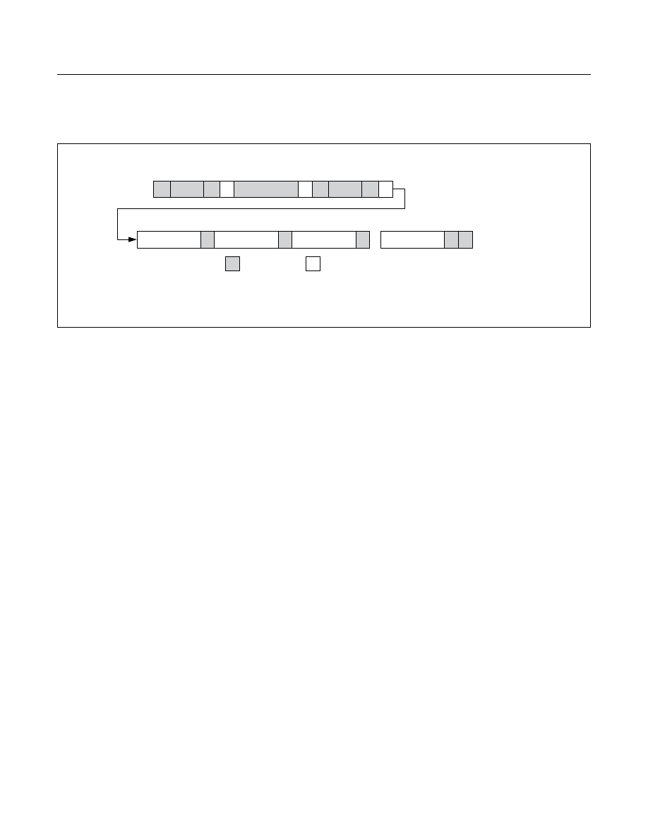
Figure 5. Data Write/Read (Write Pointer, Then Read)—Slave Receive and Transmit

S - START

Sr - REPEATED START

A - ACKNOWLEDGE (ACK)

P - STOP

A

 - NOT ACKNOWLEDGE (NACK)

R/

W

 - READ/WRITE OR DIRECTION BIT ADDRESS

<R/

W

>

<WORD ADDRESS (n)> <SLAVE ADDRESS (n)>

<SLAVE

ADDRESS>

<R/

W

>

A

XXXXXXXX

A

1101000

1101000

S

Sr

0

A

1

DATA TRANSFERRED

(X + 1 BYTES + ACKNOWLEDGE)

NOTE: LAST DATA BYTE IS FOLLOWED BY A NACK.

MASTER TO SLAVE

SLAVE TO MASTER

A

XXXXXXXX

XXXXXXXX

A

XXXXXXXX

A

XXXXXXXX

A

P

 <DATA (n)>                        <DATA (n + 1)>                       <DATA (n + 2)>                             <DATA (n + X)>

...

DS3231

Extremely Accurate I

2

C-Integrated

RTC/TCXO/Crystal

www.maximintegrated.com

Maxim Integrated  


17

Handling, PCB Layout, and Assembly

The DS3231 package contains a quartz tuning-fork 


crystal. Pick-and-place equipment can be used, but 


precautions should be taken to ensure that 


excessive shocks are avoided. Ultrasonic cleaning should be  

avoided to prevent damage to the crystal.
Avoid running signal traces under the package, unless 

a ground plane is placed between the package and the 

signal line. All N.C. (no connect) pins must be connected 

to ground.
Moisture-sensitive packages are shipped from the 


factory dry packed. Handling instructions listed on the 

package label must be followed to prevent damage during 

reflow. Refer to the IPC/JEDEC J-STD-020 standard for  

moisture-sensitive device (MSD) classifications and reflow 

profiles. Exposure to reflow is limited to 2 times maximum.

#

Denotes an RoHS-compliant device that may include lead 

(Pb) that is exempt under RoHS requirements. The lead finish 

is JESD97 category e3, and is compatible with both lead-based 

and lead-free soldering processes. A “#” anywhere on the top 

mark denotes an RoHS-compliant device.

PACKAGE 

TYPE

PACKAGE 

CODE

OUTLINE 

NO.

LAND 

PATTERN NO.

16 SO

W16#H2

21-0042

90-0107

PART

TEMP RANGE

PIN-PACKAGE

DS3231S#

 0°C to +70°C

16 SO

DS3231SN#

-40°C to +85°C

16 SO

16

15
14

13
12

11
10

9

1

2

3
4
5

6

7

8

32kHz

SCL

SDA
V

BAT

GND
N.C.

N.C.
N.C.

N.C.

TOP VIEW

SO

V

CC

INT

/SQW

N.C.

RST

N.C.

N.C.

N.C.

DS3231

DS3231

Extremely Accurate I

2

C-Integrated

RTC/TCXO/Crystal

www.maximintegrated.com

Maxim Integrated  


18

Package Information

For the latest package outline information and land patterns 

(footprints), go to 

www.maximintegrated.com/packages

. Note 

that a “+”, “#”, or “-” in the package code indicates RoHS status 

only. Package drawings may show a different suffix character, but 

the drawing pertains to the package regardless of RoHS status.

Chip Information

SUBSTRATE CONNECTED TO GROUND
PROCESS: CMOS

Pin Configuration

Ordering Information

REVISION

NUMBER

REVISION 

DATE

DESCRIPTION

PAGES

CHANGED

0

1/05

Initial release.

1

2/05

Changed Digital Temp Sensor Output from ±2°C to ±3°C.

1, 3

Updated 

Typical Operating Circuit

.

1

Changed T

A

 = -40°C to +85°C to T

A

 = T

MIN

 to T

MAX

.

2, 3, 4

Updated 

Block Diagram

.

8

2

6/05

Added “UL Recognized” to Features; added lead-free packages and removed S from top 

mark info in 

Ordering Information

 table; added ground connections to the N.C. pin in the 

Typical Operating Circuit.

1

Added “noncondensing” to operating temperature range; changed V

PF

 MIN from 2.35V to 

2.45V.

2

Added aging offset specification.

3

Relabeled TOC4.

7

Added arrow showing input on X1 in the 

Block Diagram

.

8

Updated pin descriptions for V

CC

 and V

BAT

.

9

Added the I

2

C Interface section.

10

Figure 1:

 Added sign bit to aging and temperature registers; added MSB and LSB.

11

Corrected title for rate select bits frequency table.

13

Added note that frequency stability over temperature spec is with aging offset register = 

00h; changed bit 7 from Data to Sign (Crystal Aging Offset Register).

14

Changed bit 7 from Data to Sign (Temperature Register); correct pin definitions in 

I

2

Serial Data Bus

 section.

15

Modified the 

Handing

PC Board Layout

, and 

Assembly

 section to refer to

J-STD-020 for reflow profiles for lead-free and leaded packages.

17

3

11/05

Changed lead-free packages to RoHS-compliant packages.

1

4

10/06

Changed 

RST

 and UL bullets in 

Features

.

1

Changed EC condition “V

CC

 > V

BAT

” to “V

CC

 = Active Supply (see Table 1).”

2, 3

Modified Note 12 to correct t

REC

 operation.

6

Added various conditions text to TOCs 1, 2, and 3.

7

Added text to pin descriptions for 32kHz, V

CC

, and 

RST

.

9

Table 1: Changed column heading “Powered By” to “Active Supply”; changed “applied” to 

“exceeds V

PF

” in the 

Power Control

 section.

10

Indicated BBSQW applies to both SQW and interrupts; simplified temp convert 

description (bit 5); added “output” to 

INT

/SQW (bit 2).

13

Changed the 

Crystal Aging

 section to the 

Aging Offset

 section; changed “this bit 

indicates” to “this bit controls” for the enable 32kHz output bit.

14

5

4/08

Added Warning note to EC table notes; updated Note 12.

6

Updated the 

Typical Operating Characteristics

 graphs.

7

In the 

Power Control

 section, added information about the POR state of the time and date 

registers; in the 

Real-Time Clock

 section, added to the description of the RST function.

10

In Figure 1, corrected the months date range for 04h from 00–31 to 01–31.

11

DS3231

Extremely Accurate I

2

C-Integrated

RTC/TCXO/Crystal

www.maximintegrated.com

Maxim Integrated  


19

Revision History

REVISION

NUMBER

REVISION 

DATE

DESCRIPTION

PAGES

CHANGED

6

10/08

Updated the 

Typical Operating Circuit

.

1

Removed the V

PU

 parameter from the 

Recommended DC Operating Conditions

 table 

and added verbiage about the pullup to the 

Pin Description

 table for 

INT

/SQW, SDA, and 

SCL.

2, 9

Added the Delta Time and Frequency vs. Temperature graph in the 

Typical Operating 

Characteristics

 section.

7

Updated the 

Block Diagram

.

8

Added the 

V

BAT

 Operation

 section, improved some sections of text for the 

32kHz TCXO


and 

Pushbutton Reset Function

 sections.

10

Added the register bit POR values to the register tables.

13, 14, 15

Updated the 

Aging Offset 

and 

Temperature Registers (11h–12h)

 sections.

14, 15

Updated the I

2

C timing diagrams (Figures 3, 4, and 5).

16, 17

7

3/10

Removed the “S” from the top mark in the 

Ordering Information

 table and the 

Pin 

Configuration

 to match the packaging engineering marking specification.

1, 18

8

7/10

Updated the 

Typical Operating Circuit

; removed the “Top Mark” column from the 

Ordering 

Information

; in the 

Absolute Maximum Ratings

 section, added the theta-JA and theta-

JC thermal resistances and Note 1, and changed the soldering temperature to +260°C 

(lead(Pb)-free) and +240°C (leaded); updated the functional description of the V

BAT

 pin 

in the 

Pin Description

; changed the timekeeping registers 02h, 09h, and 0Ch to “20 Hour” 

in Bit 5 of Figure 1; updated the BBSQW bit description in the 

Control Register (0Eh)


section; added the land pattern no. to the 

Package Information

 table.

1, 2, 3, 4, 6, 9, 

11, 12, 13, 18

9

1/13

Updated 

Absolute Maximum Ratings

, and last paragraph in 

Power Control 

section

2, 10

10

3/15

Revised 

Benefits and Features

 section.

1

Maxim Integrated cannot assume responsibility for use of any circuitry other than circuitry entirely embodied in a Maxim Integrated product. No circuit patent licenses 

are implied. Maxim Integrated reserves the right to change the circuitry and specifications without notice at any time. The parametric values (min and max limits) 

shown in the Electrical Characteristics table are guaranteed. 

Other parametric values quoted in this data sheet are provided for guidance.

Maxim Integrated and the Maxim Integrated logo are trademarks of Maxim Integrated Products, Inc.

DS3231

Extremely Accurate I

2

C-Integrated

RTC/TCXO/Crystal


20

Revision History (continued)

For pricing, delivery, and ordering information, please contact Maxim Direct at 1-888-629-4642, or visit Maxim Integrated’s website at www.maximintegrated.com.

Mouser Electronics


Authorized Distributor


Click to View Pricing, Inventory, Delivery & Lifecycle Information:


Maxim Integrated

:  


DS3231S#


DS3231S#T&R


DS3231SN#


DS3231SN#T&R


DS3231S


DS3231SN


DS3231S/T&R


DS3231SN/T&R


DS3231S#-W

1/26

¡ Semiconductor

MSM82C51A-2RS/GS/JS

GENERAL  DESCRIPTION

The MSM82C51A-2 is a USART (Universal Synchronous Asynchronous Receiver Transmitter)

for serial data communication.
As a peripheral device of a microcomputer system, the MSM82C51A-2 receives parallel data

from the CPU and transmits serial data after conversion.  This device also receives serial data

from the outside and transmits parallel data to the CPU after conversion.

The  MSM82C51A-2  configures  a  fully  static  circuit  using  silicon  gate  CMOS  technology.

Therefore,  it  operates  on  extremely  low  power  at  100 

m

A  (max)  of  standby  current  by

suspending all operations.

FEATURES

• Wide power supply voltage range from 3 V to 6 V
• Wide temperature range from –40

°

C to 85

°

C

• Synchronous communication upto 64 Kbaud
• Asynchronous communication upto 38.4 Kbaud
• Transmitting/receiving operations under double buffered configuration.
• Error detection (parity, overrun and framing)
• 28-pin Plastic DIP (DIP28-P-600-2.54): (Product name: MSM82C51A-2RS)
• 28-pin Plastic QFJ (QFJ28-P-S450-1.27): (Product name: MSM82C51A-2JS)

• 32-pin Plastic SSOP(SSOP32-P-430-1.00-K): (Product name: MSM82C51A-2GS-K)

¡ Semiconductor

MSM82C51A-2RS/GS/JS

UNIVERSAL SYNCHRONOUS ASYNCHRONOUS RECEIVER TRANSMITTER

E2O0017-27-X2

This version:  Jan. 1998

Previous version:  Aug. 1996

2/26

¡ Semiconductor

MSM82C51A-2RS/GS/JS

FUNCTIONAL  BLOCK  DIAGRAM

TXD

D

7 - 

D

0

RESET

CLK

 C/

D

RD

WR

CS

DSR

DTR

CTS

RTS

Read/Write

Control

Logic

Modem

Control

Transmit

Buffer

(P - S)

Transmit

Control

Recieve

Buffer

(S - P)

Recieve

Control

TXRDY
TXE

TXC

RXD

RXRDY

RXC

SYNDET/BD

Data Bus

Buffer

Internal Bus Line

3/26

¡ Semiconductor

MSM82C51A-2RS/GS/JS

PIN  CONFIGURATION (TOP VIEW)

D

1

D

0

V

CC

RXC
DTR
RTS
DSR

RESET

CLK

TXD

TXEMPTY

CTS

SYNDET/BD

TXRDY

1

2

3

4

5

6

7

8

9

10

11

12

28

27

26

25

24

23

22

21
20

19

18

17

13

14

16

15

28 pin Plastic DIP

D

7

D

6

D

5

GND

RXD

D

4

D

3

D

2

WR

CS

C/

D

RD

RXRDY

TXC

32 pin Plastic SSOP

16

15

14

13

NC

D

7

D

6

D

5

GND

RXD

D

4

D

3

D

2

D

1

D

0

WR

CS

NC

C/

D

RD

RXRDY

V

CC

RXC

TXC

NC

DTR
RTS
DSR

RESET

CLK

TXD

TXEMPTY

NC

CTS

SYNDET/BD

TXRDY

1

2

3

4

5

6

7

8

9

10

11

12

24

23

22

21

20

19

18

29

30

31

32

28

27

26

25

17

25
24
23
22
21
20
19

RXC
DTR
RTS
DSR

RESET
CLK
TXD

D

4

D

5

D

6

D

7

TXC

WR

CS

12

13

14

15

16

17

18

C/

D

RD

RXRDY

TXRDY

SYNDET/BD

CTS

TXEMPTY

4

3

2

1

28

27

26

GND

RXD

D

3

D

2

D

1

D

0

5
6
7
8
9

10
11

V

CC

28 pin Plastic QFJ

4/26

¡ Semiconductor

MSM82C51A-2RS/GS/JS

FUNCTION

Outline

The MSM82C51A-2's functional configuration is programed by software.

Operation between the MSM82C51A-2 and a CPU is executed by program control.  Table 1

shows the operation between a CPU and the device.

0
0
0

Data Bus 3-State

1

Data Bus 3-State

CS

¥

1
1

¥

C/

D

Status 

Æ

 CPU

Control Word 

¨

 CPU

1
1
0

¥

0

Data 

¨

 CPU

0

Data 

Æ

 CPU

0

0

0

1

WR

1
0
1

¥

1

0

RD

Table 1  Operation between MSM82C51A and CPU

It is necessary to execute a function-setting sequence after resetting the MSM82C51A-2. Fig. 1

shows the function-setting sequence.
If the function was set, the device is ready to receive a command, thus enabling the transfer of

data  by setting a necessary command, reading a status and reading/writing data.

Asynchronous

External Reset

Internal Reset

Write Mode Instruction

Write First Sync 

Charactor

yes

no

Single

Sync Mode

Write Second Sync

Charactor

yes

no

End of Mode Setting

Fig. 1  Function-setting Sequence (Mode Instruction Sequence)

5/26

¡ Semiconductor

MSM82C51A-2RS/GS/JS

Control Words

There are two types of control word.
1. Mode instruction (setting of function)
2. Command (setting of operation)

1) Mode Instruction

Mode instruction is used for setting the function of the MSM82C51A-2.  Mode instruction

will be in “wait for write” at either internal reset or external reset.  That is, the writing of a

control word after resetting will be recognized as a “mode instruction.”

Items set by mode instruction are as follows:

Synchronous/asynchronous mode

Stop bit length (asynchronous mode)

Character length

Parity bit

Baud rate factor (asynchronous mode)

Internal/external synchronization (synchronous mode)

Number of synchronous characters (Synchronous mode)

The  bit  configuration  of  mode  instruction  is  shown  in  Figures  2  and  3.    In  the  case  of

synchronous mode, it is necessary to write one-or two byte sync characters.
If sync characters were written, a function will be set because the writing of sync characters

constitutes part of mode instruction.

S

1

S

1

EP

PEN

L

2

L

1

B

2

B

1

D

7

D

6

D

5

D

4

D

3

D

2

D

1

D

0

0

1

0

1

0

0

1

1

Refer to

Fig. 3

SYNC

¥

16 

¥

64 

¥

Baud Rate Factor

0

1

0

0

0

1

5 bits

6 bits

7 bits

Charactor Length

1
1

8 bits

0

1

0

1

0

0

1

1

Disable

Odd

Parity

Disable

Even

Parity

Parity Check

0

1

0

0

0

1

Inhabit

1 bit

1.5 bits

Stop bit Length

1
1

2 bits

Fig. 2  Bit Configuration of Mode Instruction (Asynchronous)

6/26

¡ Semiconductor

MSM82C51A-2RS/GS/JS

D

7

D

6

D

5

D

4

D

3

D

2

D

1

D

0

SCS

ESD

EP

PEN

L

2

L

1

0

0

Charactor Length

0

1

0

0

0

1

5 bits

6 bits

7 bits

1
1

8 bits

0

1

0

1

0

0

1

1

Disable

Odd

Parity

Disable

Even

Parity

Parity

0

1

Internal

Synchronization

External

Synchronization

Synchronous Mode

0

1

2 Charactors

1 Charactor

Number of Synchronous Charactors

Fig. 3  Bit Configuration of Mode Instruction (Synchronous)

7/26

¡ Semiconductor

MSM82C51A-2RS/GS/JS

2) Command

Command is used for setting the operation of the MSM82C51A-2.
It is possible to write a command whenever necessary after writing a mode instruction and

sync characters.
Items to be set by command are as follows:

Transmit

Enable/Disable

Receive Enable/Disable

DTR

RTS

Output of data.

Resetting of error flag.

Sending to break characters

Internal resetting

Hunt mode (synchronous mode)

The bit configuration of a command is shown in Fig. 4.

EH

D

7

IR

D

6

RTS

D

5

ER

D

4

SBRK

D

3

RXE

D

2

DTR

D

1

TXEN

D

0

1

º

Transmit Enable

0

º

Disable

DTR

1  

Æ


DTR

 = 0

0  

Æ


DTR

 = 1

1

º

Recieve Enable

0

º

Disable

1

º

Sent Break Charactor

0

º

Normal Operation

1

º

Reset Error Flag

0

º

Normal Operation

RTS

1  

Æ


RTS

 = 0

0  

Æ


RTS

 = 1

1

º

Internal Reset

0

º

Normal Operation

1

º

Hunt Mode (Note)

0

º

Normal Operation

Note

:  Seach mode for synchronous

charactors in synchronous mode.

Fig. 4  Bit Configuration of Command

8/26

¡ Semiconductor

MSM82C51A-2RS/GS/JS

Status Word

It is possible to see the internal status of MSM82C51A-2 by reading a status word.
The bit configuration of status word is shown in Fig. 5.

Same as terminal.

Refer to "Explanation" 

of Terminals.

DSR

D

7

SYNDET

/BD

D

6

FE

D

5

OE

D

4

PE

D

3

TXEMPTY

D

2

RXRDY

D

1

TXRDY

D

0

Parity Different from 

TXRDY Terminal.

Refer to "Explanation" 

of TXRDY Terminals.

1

º

Parity Error

1

º

Overrun Error

1

º

Framing Error

 Note:


Shows Terminal 

DSR

1

º

DSR

 = 0

0

º

DSR

 = 1 

Only asynchronous mode.

Stop bit cannot be detected.

Fig. 5  Bit Configuration of Status Word

Standby Status

It is possible to put the MSM82C51A-2 in “standby status”
When the following conditions have been satisfied the MSM82C51A-2 is in “standby status.”

(1)

CS 

terminal is fixed at Vcc level.

(2) Input pins other 

CS 

, D

0

 to D

7

RD

WR 

and C/

D

 are fixed at Vcc or GND level (including

SYNDET in external synchronous mode).

Note:

When all output currents are 0, ICCS specification is applied.

9/26

¡ Semiconductor

MSM82C51A-2RS/GS/JS

Pin Description

D

0

 to D

7

 (l/O terminal)

This is bidirectional data bus which receive control words and transmits data from the CPU and

sends status words and received data to CPU.

RESET (Input terminal)

A “High” on this input forces the MSM82C51A-2 into “reset status.”
The device waits for the writing of “mode instruction.”
The min. reset width is six clock inputs during the operating status of CLK.

CLK (Input terminal)

CLK signal is used to generate internal device timing.
CLK signal is independent of 

RXC

 or 

TXC

.

However, the frequency of CLK must be greater than 30 times the 

RXC

 and 

TXC

 at Synchronous

mode and Asynchronous “x1” mode, and must be greater than 5 times at Asynchronous “x16”

and “x64” mode.

WR

 (Input terminal)

This is the “active low” input terminal which receives a signal for writing transmit data and

control words from the CPU into the MSM82C51A-2.

RD

 (Input terminal)

This is the “active low” input terminal which receives a signal for reading receive data and

status words from the MSM82C51A-2.

C/

D

 (Input terminal)

This is an input terminal which receives a signal for selecting data or command words and status

words when the MSM82C51A-2 is accessed by the CPU.
If C/

D

 = low, data will be accessed.

If C/

D

 = high, command word or status word will be accessed.

CS

 (Input terminal)

This is the “active low” input terminal which selects the MSM82C51A-2 at low level when the

CPU accesses.

Note:

The device won’t be in “standby status”; only setting 

CS

 = High.

Refer to “Explanation of Standby Status.”

TXD (output terminal)

This is an output terminal for transmitting data from which serial-converted data is sent out.

The device is in “mark status” (high level) after resetting or during a status when transmit is

disabled.  It is also possible to set the device in “break status” (low level) by a command.

10/26

¡ Semiconductor

MSM82C51A-2RS/GS/JS

TXRDY (output terminal)

This  is  an  output  terminal  which  indicates  that  the  MSM82C51A-2  is  ready  to  accept  a

transmitted data character.  But the terminal is always at low level if 

CTS

 = high or the device

was set in “TX disable status” by a command.

Note: TXRDY  status  word  indicates  that  transmit  data  character  is  receivable,

regardless

of 

CTS

 or command.

If the CPU writes a data character, TXRDY will be reset by the leading edge or 

WR

signal.

TXEMPTY (Output terminal)

This  is  an  output  terminal  which  indicates  that  the  MSM82C51A-2  has  transmitted  all  the

characters and had no data character.
In “synchronous mode,” the terminal is at high level, if transmit data characters are no longer

remaining  and  sync  characters  are  automatically  transmitted.    If  the  CPU  writes  a  data

character, TXEMPTY will be reset by the leading edge of 

WR

 signal.

Note : As the transmitter is disabled by setting 

CTS

 “High” or command, data written

before disable will be sent out.  Then TXD and TXEMPTY will be “High”.
Even  if  a  data  is  written  after  disable,  that  data  is  not  sent  out  and  TXE  will  be

“High”.After

the  transmitter  is  enabled,  it  sent  out.    (Refer  to  Timing  Chart  of

Transmitter Control and Flag

Timing)

TXC

 (Input terminal)

This is a clock input signal which determines the transfer speed of transmitted data.

In “synchronous mode,” the baud rate will be the same as the frequency of 

TXC

.

In “asynchronous mode”, it is possible to select the baud rate factor by mode instruction.
It can be 1, 1/16 or 1/64 the 

TXC

.

The falling edge of 

TXC

 sifts the serial data out of the MSM82C51A-2.

RXD (input terminal)

This is a terminal which receives serial data.

RXRDY (Output terminal)

This is a terminal which indicates that the MSM82C51A-2 contains a character that is ready to

READ.
If the CPU reads a data character, RXRDY will be reset by the leading edge of 

RD

 signal.

Unless the CPU reads a data character before the next one is received completely, the preceding

data will be lost.  In such a case, an overrun error flag status word will be set.

RXC

 (Input terminal)

This is a clock input signal which determines the transfer speed of received data.

In “synchronous mode,” the baud rate is the same as the frequency of 

RXC

.

In “asynchronous mode,” it is possible to select the baud rate factor by mode instruction.
It can be 1, 1/16, 1/64 the 

RXC

.

11/26

¡ Semiconductor

MSM82C51A-2RS/GS/JS

SYNDET/BD (Input or output terminal)

This is a terminal whose function changes according to mode.

In “internal synchronous mode.” this terminal is at high level, if sync characters are received and

synchronized.  If a status word is read, the terminal will be reset.
In “external synchronous mode, “this is an input terminal.
A “High” on this input forces the MSM82C51A-2 to start receiving data characters.
In “asynchronous mode,” this is an output terminal which generates “high level”output upon

the detection of a “break” character if receiver data contains a “low-level” space between the

stop bits of two continuous characters.  The terminal will be reset, if RXD is at high level.
After Reset is active, the terminal will be output at low level.

DSR

 (Input terminal)

This is an input port for MODEM interface.  The input status of the terminal can be recognized

by the CPU reading status words.

DTR

 (Output terminal)

This is an output port for MODEM interface.  It is possible to set the status of 

DTR

 by a command.

CTS

 (Input terminal)

This is an input terminal for MODEM interface which is used for controlling a transmit circuit.

The terminal controls data transmission if the device is set in “TX Enable” status by a command.

Data is transmitable if the terminal is at low level.

RTS

 (Output terminal)

This is an output port for MODEM interface.  It is possible to set the status 

RTS

 by a command.


содержание      ..     3      4      5      6     ..